 | –≠–ª–µ–∫—Ç—Ä–æ–Ω–Ω—ã–π –∫–æ–º–ø–æ–Ω–µ–Ω—Ç: LTC3401 | –°–∫–∞—á–∞—Ç—å:  PDF PDF  ZIP ZIP |
LTC3428
1
3428f
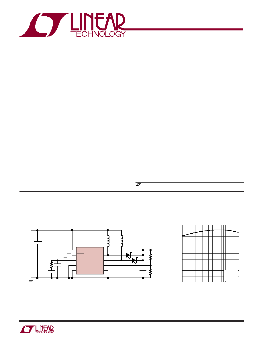
The LTC
Æ
3428 is a 2-phase, current mode boost con-
verter, capable of supplying 2A at 5V from a 3.3V input.
Two 93m, 2A N-channel MOSFET switches allow the
LTC3428 to deliver high efficiency from input voltages as
low as 1.6V.
External parts count and size are minimized by a 1MHz
switching frequency and a 2-phase design. Two phase
operation significantly reduces peak inductor currents
and capacitor ripple current, doubling the effective switch-
ing frequency and minimizing inductor and capacitor size.
External compensation allows the feedback loop response
to be optimized for a particular application.
Other features include: an active low shutdown pin re-
duces supply current to below 1µA, internal soft-start,
antiringing control and thermal shutdown. The LTC3428
is available in a low profile (0.75mm) 10-lead (3mm ◊
3mm) DFN package.
FEATURES
DESCRIPTIO
U
APPLICATIO S
U
TYPICAL APPLICATIO
U
Networking Equipment
Handheld Instruments
Digital Cameras
Distributed Power
Local 3.3V to 5V Conversion
, LTC and LT are registered trademarks of Linear Technology Corporation.
V
OUT
SWA
SWB
FB
PGNDB
V
IN
SHDN
V
C
AGND
PGNDA
LTC3428
383k
121k
22µF****
22pF
10k
1000pF
4.7µF***
V
IN
3.3V
V
OUT
5V/2A
3428 TA01
2.2µH*
2.2µH*
OFF ON
TOKO FDV06302R2
PHILIPS PMEG1020
TAIYO YUDEN X5R JMK212BJ475MD
TAIYO YUDEN X5R JMK316BJ226ML
*
**
***
****
**
**
Efficiency vs Load Current
3.3V to 5V at 2A Converter
High Efficiency: Up to 92%
2-Phase Control Reduces Output Voltage Ripple
5V at 2A from 3.3V Input
3.3V at 1.5A from 1.8V Input
1.6V to 5.25V Adjustable Output Voltage
1.6V to 4.5V Input Range
Internal Soft-Start Operation
Low Shutdown Current: <1µA
Uses Small Surface Mount Components
10-Pin 3mm ◊ 3mm DFN Package
4A, 2MHz Dual Phase
Step-Up DC/DC Converter
in 3mm ◊ 3mm DFN
LOAD CURRENT (A)
0.1
EFFICIENCY (%)
95
90
85
80
75
70
65
60
55
50
45
1
2
3428 TA02
V
IN
= 3.3V
V
OUT
= 5V
L = 2.2µH
LTC3428
2
3428f
V
IN
, V
OUT
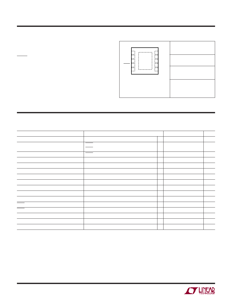
, SWA, SWB Voltage ....................... ≠ 0.3 to 6V
SWA, SWB Voltage, Pulsed, <100ns ......................... 7V
SHDN, VC Voltage ......................................... ≠ 0.3 to 6V
FB Voltage ................................... ≠ 0.3 to (V
OUT
+ 0.3V)
Operating Temperature Range (Note 2) .. ≠ 40∞C to 85∞C
Storage Temperature Range ..................≠65∞C to 125∞C
ORDER PART
NUMBER
DD PART
MARKING
T
JMAX
= 125∞C,
JA
= 45∞C/W,
JC
= 3∞C/W
Consult LTC Marketing for parts specified with wider operating temperature ranges.
LBBG
ABSOLUTE AXI U
RATI GS
W
W
W
U
PACKAGE/ORDER I FOR ATIO
U
U
W
(Note 1)
ELECTRICAL CHARACTERISTICS
Note 1: Absolute Maximum Ratings are those values beyond which the life
of a device may be impaired.
Note 2: The LTC3428E is guaranteed to meet performance specifications
from 0∞C to 70∞C. Specifications over the ≠40∞C to 85∞C operating
temperature range are assured by design, characterization and correlation
with statistical process controls.
The
denotes the specifications which apply over the full operating
temperature range, otherwise specifications are at T
A
= 25∞C. V
IN
= 3.3V, V
OUT
= 5V unless otherwise noted.
PARAMETER
CONDITIONS
MIN
TYP
MAX
UNITS
Minimum Startup Voltage
1.5
1.6
V
Quiescent Current, V
OUT
SHDN = V
IN
100
200
µA
Quiescent Current, V
IN
SHDN = V
IN
1.3
2.0
mA
Shutdown Current
SHDN = 0V
1
µA
Switching Frequency
Per Phase
0.8
1.0
1.2
MHz
FB Regulated Voltage
1.219
1.243
1.268
V
FB Input Current
V
FB
= 1.24V
1
50
nA
Error Amp Transconductance
170
µS
Output Adjust Voltage
1.6
5.25
V
NMOS Switch Leakage
V
SWA
, V
SWB
= 5.5V, Per Phase
0.1
2.5
µA
NMOS Switch On Resistance
V
OUT
= 5V, Per Phase
0.093
NMOS Current Limit
Per Phase
2
2.5
A
SHDN Input Threshold
0.4
0.8
1.5
V
SHDN Input Current
0.01
1
µA
Maximum Duty Cycle
80
87
%
Minimum Duty Cycle
0
%
Current Limit Delay to Output
(Note 3)
40
ns
Note 3: Specification is guaranteed by design and not 100% tested in
production.
Note 4: This IC includes overtemperature protection that is intended to
protect the device during momentary overload conditions. Junction
temperature will exceed 125∞C when overtemperature protection is active.
Continuous operation above the specified maximum operating junction
temperature may impair device reliability.
TOP VIEW
DD PACKAGE
10-LEAD (3mm ◊ 3mm) PLASTIC DFN
EXPOSED PAD MUST BE SOLDERED
TO GROUND PLANE ON PCB
10
9
6
7
8
4
5
3
2
1
PGNDB
SWB
V
IN
AGND
FB
PGNDA
SWA
V
OUT
SHDN
V
C
11
LTC3428EDD
LTC3428
3
3428f
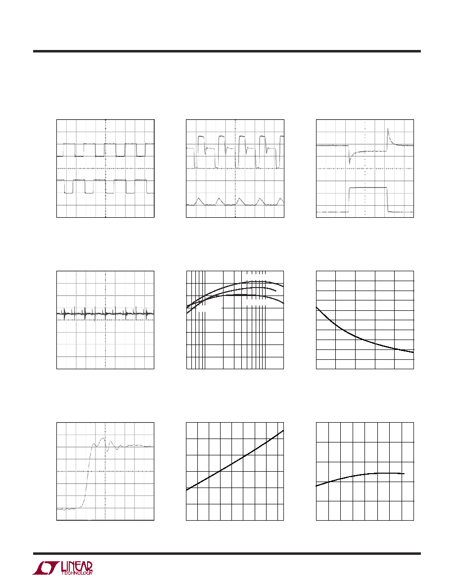
TYPICAL PERFOR A CE CHARACTERISTICS
U
W
3428 G09
LOAD CURRENT (A)
0.05
EFFICIENCY (%)
95
90
85
80
75
70
65
60
55
0.1
1
2
3428 G05
3428 G04
3.3V TO 5V
2.5V TO 3.3V
2.5V TO 5V
OUTPUT VOLTAGE (V)
2.5
R
DS(ON)
(m
)
108
106
104
102
100
98
96
94
92
90
88
4.5
3428 G06
3428 G02
3428 G01
3428 G03
3.0
3.5
4.0
5.0
R
DS(ON)
(m
)
120
110
100
90
80
70
60
FB VOLTAGE (V)
1.27
1.26
1.25
1.24
1.23
1.22
3428 G08
TEMPERATURE (∞C)
3428 G07
10ns/DIV
≠45
15
55
115
≠25 ≠5
35
75
95
TEMPERATURE (∞C)
≠45
15
55
115
≠25
≠5
35
75
95
500ns/DIV
500ns/DIV
500ns/DIV
100µs/DIV
5V/DIV
50mV/DIV
1V/DIV
2V/DIV
500mA/DIV
100mV/DIV
500mA/DIV
SWA
SWB
SWA, SWB Switching Waveforms
SWA, SWB Rise Time, I = 2A
Switch R
DS(ON)
vs V
OUT
Converter Efficiency
Output Voltage Ripple with 22µF
Ceramic Capacitor
Transient Response, 0.5A to 1.5A
SW Pin and Inductor Current in
Discontinuous Mode, Demonstrating
Anti-Ring Circuit Operation
Switch R
DS(ON)
vs Temperature
Feedback Voltage vs Temperature
All characteristic curves at T
A
= 25∞C unless otherwise noted.
LTC3428
4
3428f
PI FU CTIO S
U
U
U
PGNDA, PGNDB (Pins 1, 10, 11 (Exposed Pad)): Power
Ground for the IC. Tie directly to local ground plane.
SWB (Pin 2), SWA (Pin 9): Phase B and Phase A Switch
Pins. The inductor and Schottky diodes for each phase are
connected to these pins. Minimize trace length to reduce
EMI.
V
OUT
(Pin 3): Power Supply Output and Bootstrapped
Power Source for the IC. Connect low ESR output filter
capacitors from this pin to the ground plane.
SHDN (Pin 4): Shutdown Pin. Grounding this pin shuts
down the IC. Connect to a voltage greater than 1.5V to
enable.
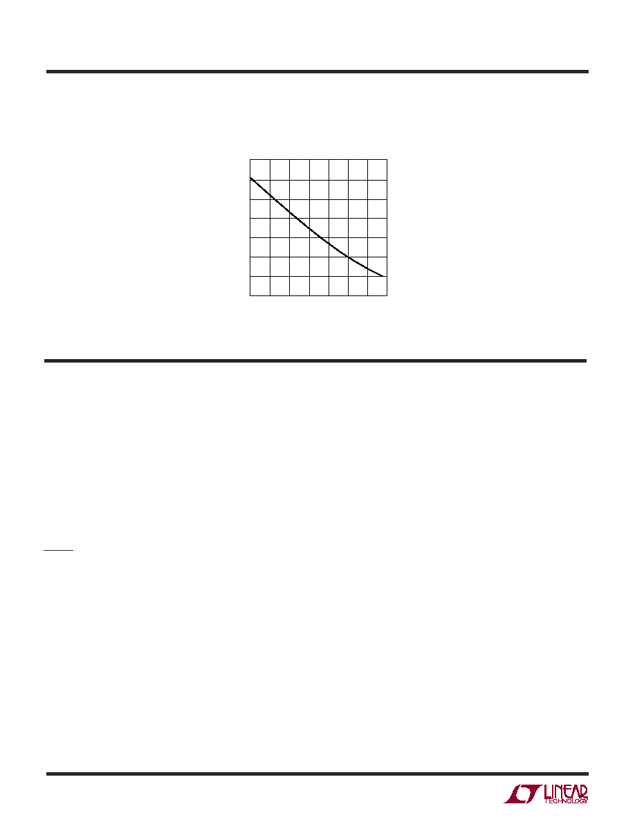
TYPICAL PERFOR A CE CHARACTERISTICS
U
W
PEAK CURRENT LIMIT (A)
3.4
3.2
3.0
2.8
2.6
2.4
2.2
2.0
3428 G10
TEMPERATURE (∞C)
≠45
15
55
≠25
≠5
35
75
95
Peak Current Limit vs
Temperature
V
C
(Pin 5): Error Amp Output. A frequency compensation
network is connected to this pin to compensate the boost
converter loop.
FB (Pin 6): Feedback Pin. A resistor divider from V
OUT
is
connected here to set the output voltage according to
V
OUT
= 1.243 ∑ (1 + R1 / R2)
AGND (Pin 7): Signal Ground for the IC. Connect to ground
plane near feedback resistor divider.
V
IN
(Pin 8): Input Supply Pin. Bypass V
IN
with a low ESR
ceramic capacitor of at least 4.7µF. X5R and X7R dielec-
trics are preferred for their superior voltage and tempera-
ture characteristics.
LTC3428
5
3428f
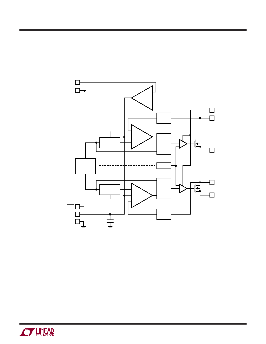
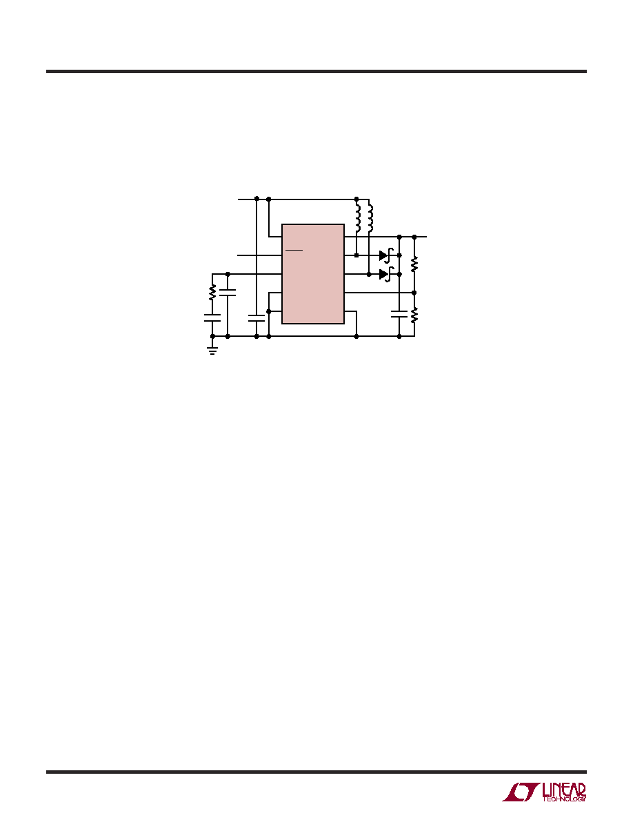
BLOCK DIAGRA
W
≠
+
≠
+
≠
PWM
COMP
+
≠
≠
PWM
COMP
PWM
LOGIC
PWM
LOGIC
TSD
CURRENT
LIMIT
CURRENT
LIMIT
1.243V
V
C
ERROR AMPLIFIER/SOFT-START
RAMP/
SLOPE COMP
OSCILLATOR
CLK B
CLK A
CHANNEL B
CHANNEL A
RAMP/
SLOPE COMP
I
SENA
I
SENB
FB
DRIVER
DRIVER
I
SENA
I
SENB
SWB
V
OUT
PGNDB
SWA
PGNDA
V
C
SHDN
SHUTDOWN
AGND
3428 BD
V
IN
FB
5pF
LTC3428
6
3428f
DETAILED DESCRIPTION
The LTC3428 provides high efficiency, low noise power
for high current boost applications. A current mode archi-
tecture with adaptive slope compensation provides both
simple loop compensation as well as excellent transient
response. The low R
DS(ON)
switches provide the pulse
width modulation control at high efficiency.
Oscillator: The per phase switching frequency is internally
set to a nominal value of 1MHz.
Current Sensing: Lossless current sensing converts the
peak current signal to a voltage which is summed with the
internal slope compensation. This summed signal is then
compared with the error amplifier output to provide a peak
current command for the PWM. Slope compensation is
internal to the IC and adapts to changes to the input
voltage, allowing the converter to provide the necessary
degree of slope compensation without causing a loss in
phase margin in the loop characteristic.
Error Amplifier: The error amplifier is a transconductance
amplifier with a transconductance (g
m
) = 1/7.5k. A
simple compensation network is placed from V
C
to ground.
The internal 5pF capacitor between V
C
and ground will
often simplify the external network to a simple R-C com-
bination. The internal 1.243V reference voltage is com-
pared to the voltage on FB to generate an error signal at the
output of the error amplifier (V
C
). A voltage divider from
V
OUT
to ground programs the output voltage from 1.6V to
5.25V using the equation:
V
OUT
= 1.243V ∑ ( 1+ R1/R2)
Soft-Start: An internal soft-start of approximately 1.5ms
is provided. This is a ramp signal that limits the peak
current until the internal soft-start voltage is greater than
the internal current limit voltage. The internal soft-start
capacitor is automatically discharged when the part is in
shutdown mode.
Current Limit: The current limit comparator in each phase
will shut off the N-channel MOSFET switches once the
current exceeds the current limit threshold, nominally
2.5A. The current limit delay to output is typically 50ns.
The current signal leading edge is blanked for 50ns to
enhance noise rejection.
Anti-Ringing Control: The antiringing control places an
impedance across the inductor of each phase to damp the
high frequency ringing on the SWA, SWB pins during
discontinuous mode operation. The LC ringing on the
switch pin due to the inductor and switch pin capacitance
is low energy, but can cause EMI radiation.
2-Phase Operation
The LTC3428 uses a two-phase architecture, rather than
the conventional single phase architecture used in most
other boost converters. The two phases are spaced 180∞
apart. Two phase operation doubles the output ripple
frequency and provides a significant reduction in output
ripple current, minimizing the stress on the output capaci-
tor. Inductor (input) peak and ripple currents are also
reduced, allowing for the use of smaller, lower cost
inductors. The greatly reduced output ripple current also
minimizes the output capacitance requirement. The higher
frequency output ripple is easier to filter for lower noise
applications.
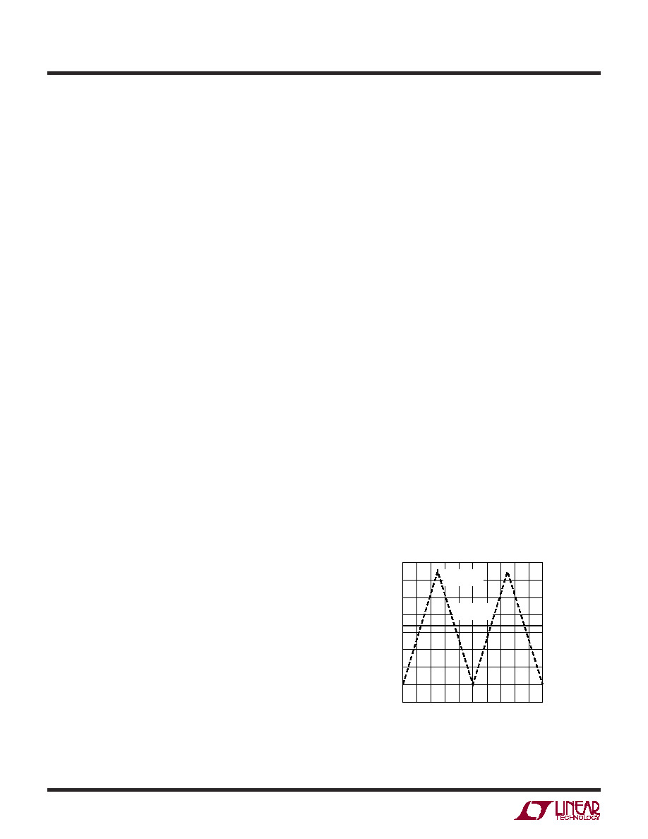
Input and output current comparisons for single and
2-phase converters are illustrated in Figures 1 and 2.
For the example illustrated in Figure 2, peak-to-peak
output ripple current was reduced by 85%, from 4.34A, to
0.64A, and peak inductor current was reduced by 53%,
from 4.34A to 2.02A. These reductions enable the use of
low profile, smaller valued inductors and output capaci-
tors as compared to a single-phase design.
APPLICATIO S I FOR ATIO
W
U
U
U
Figure 1. Input Ripple Current Comparison
Between Single Phase and Two-Phase Boost
Converters with a 2A Load and 50% Duty Cycle
TIME (µs)
0
INPUT CURRENT (A)
4.4
4.3
4.2
4.1
4.0
3.9
3.8
3.7
3.6
1.6
3428 F01
0.4
0.2
0.6
1.0
1.4
1.8
0.8
1.2
2.0
1 PHASE
CONVERTER
2 PHASE
CONVERTER
LTC3428
7
3428f
COMPONENT SELECTION
Inductor Selection
The high frequency operation of the LTC3428 allows for
the use of small surface mount inductors. The inductor
ripple current is typically set to between 20% and 40% of
the maximum inductor current. For a given set of condi-
tions, the inductance is given as follows:
L
V
V
V
R V
L
H
IN MIN
OUT
IN MIN
OUT
>
(
)
(
)
∑ (
≠
)
∑
,
2µ
where:
R = Allowable inductor current ripple (Amps P-P)
V
IN(MIN)
= Minimum input voltage (V)
V
OUT
= Output voltage (V)
For high efficiency, the inductor should have a high
frequency core material, such as ferrite, to reduce core
losses. The inductor should have a low ESR (equivalent
series resistance) to reduce I
2
R losses and must be able
to handle the peak inductor current without saturating.
Use of a toroid, pot core, or shielded bobbin inductor will
minimize radiated noise. See Table 1 for a list of inductor
manufacturers. Some example inductor part types are:
Coilcraft 1608 and 3316 series, Murata LQH55D series,
APPLICATIO S I FOR ATIO
W
U
U
U
Sumida CDRH4D22C/LD or CDRH5D28 series, Toko
FDV0630 or D62CB series.
Table 1. Inductor Vendor Information
Supplier
Phone
Fax
Website
Coilcraft
(847) 639-6400 (847) 639-1469
www.coilcraft.com
Murata
USA:
USA:
www.murata.com
(814) 238-1431 (814) 238-0490
Sumida
USA:
USA:
www.sumida.com
(847) 956-6666 (847) 956-0702
Japan:
Japan:
81-3-3607-5111 81-3-3607-5144
TDK
(847) 803-6100 (847) 803-6296
www.component.tdk.com
Toko
(847) 299-0070 (847) 699-7864
www.toko.com
Wurth
(201)785-8800
(201)785-8810
www.we-online.com
Output Capacitor Selection
The minimum value of the capacitor is set to reduce the
output ripple voltage due to charging and discharging the
capacitor each cycle. The steady state ripple due to this
charging is given by:
V
I
V
V
C
V
f
RIPPLE C
PEAK
OUT
IN MIN
OUT
OUT
( )
(
)
∑
∑ (
≠
)
∑
∑
=
1
2
where: I
PEAK
= Peak inductor current (A)
The equivalent series resistance (ESR) of the output
capacitor will contribute another term to output voltage
ripple. Ripple voltage due to capacitor ESR is:
V
I
R
RIPPLE ESR
PEAK
ESR C
(
)
( )
∑
=
where:
R
ESR(C)
= Capacitor ESR
The ESL (Equivalent Series Inductance) is another
capacitor characteristic that needs to be minimized. ESL
will be minimized by using small surface mount ceramic
capacitors, placed as close to the V
OUT
pin as possible.
Input Capacitor Selection
Since the V
IN
pin directly powers most of the internal
circuitry, it is recommended to place at least a 4.7µF, low
ESR bypass capacitor between V
IN
and AGND, as close to
the IC as possible. See Table 2 for a list of capacitor
manufacturers.
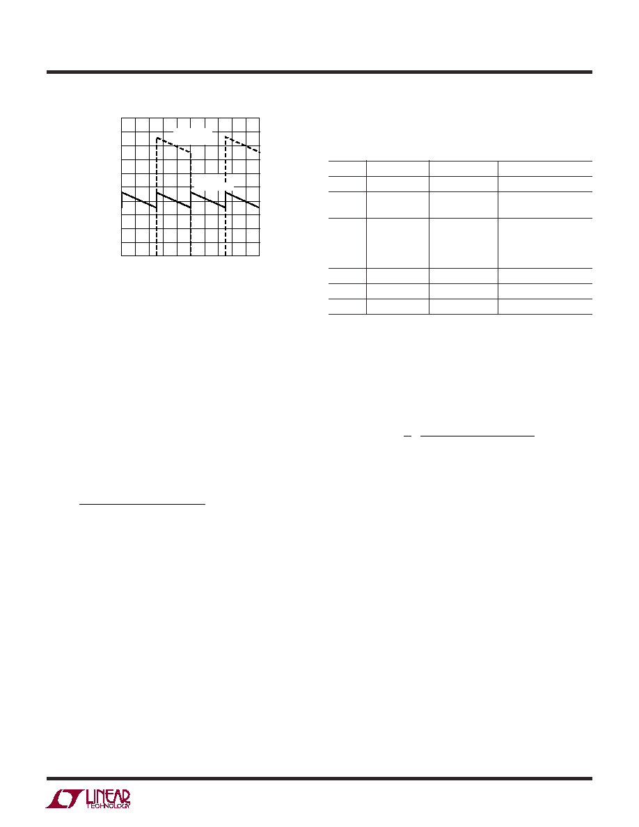
Figure 2. Output Ripple Current Comparison
Between Single Phase and Two Phase Boost
Converters with a 2A Load and 50% Duty Cycle
TIME (µs)
0
1.6
3428 F02
0.4
0.2
0.6
1.0
1.4
1.8
0.8
1.2
2.0
5.0
4.5
4.0
3.5
3.0
2.5
2.0
1.5
1.0
0.5
0
OUTPUT (DIODE) CURRENT (A)
1 PHASE
CONVERTER
2 PHASE
CONVERTER
LTC3428
8
3428f
Table 2. Capacitor Vendor Information
Supplier
Phone
Fax
Website
AVX
(803) 448-9411 (803) 448-1943 www.avxcorp.com
Sanyo
(619) 661-9322 (619) 661-1055 www.sanyovideo.com
TDK
(847) 803-6100 (847) 803-6296 www.component.tdk.com
Murata
(814) 237-1431 (814) 238-0490 www.murata.com
Taiyo Yuden (408) 573-4150 (408) 573-4159 www.t-yuden.com
Output Diode Selection
For high efficiency, a fast switching diode with low reverse
leakage and a low forward drop is required. Schottky diodes
are recommended for their low forward drop and fast
switching times. When selecting a diode, it is important to
remember that the average diode current in a boost
converter is equal to the average load current: I
D
= I
LOAD
When selecting a diode, make sure that the peak
forward current and average power dissipation ratings
meet the application requirements. See Table 3 for a list
of Schottky diode manufacturers. Example diodes are
Philips PMEG1020, PMEG2010, On-Semi MBRA210, IR
10BQ015, Microsemi UPS120E, UPS315.
Table 3. Diode Vendor Information
Supplier
Phone
Fax
Website
Philips
+31 40 27 24825
www.philips.com
Microsemi
(949) 221-7100
(949)756-0308
www.microsemi.com
On-Semi
(602) 244-6600
www.onsemi.com
International (310) 469-2161
(310) 322-3332
www.irf.com
Rectifier
Thermal Considerations
To deliver maximum power, it is necessary to provide a
good thermal path to dissipate the heat generated within
the LTC3428's package. The large thermal pad on the IC
underside can accomplish this requirement. Use multiple
PC board vias to conduct heat from the IC and to a copper
plane that has as much area as possible.
APPLICATIO S I FOR ATIO
W
U
U
U
If the junction temperature gets too high, the LTC3428 will
stop all switching until the junction temperature drops to
safe levels. The typical over temperature threshold is
150∞C.
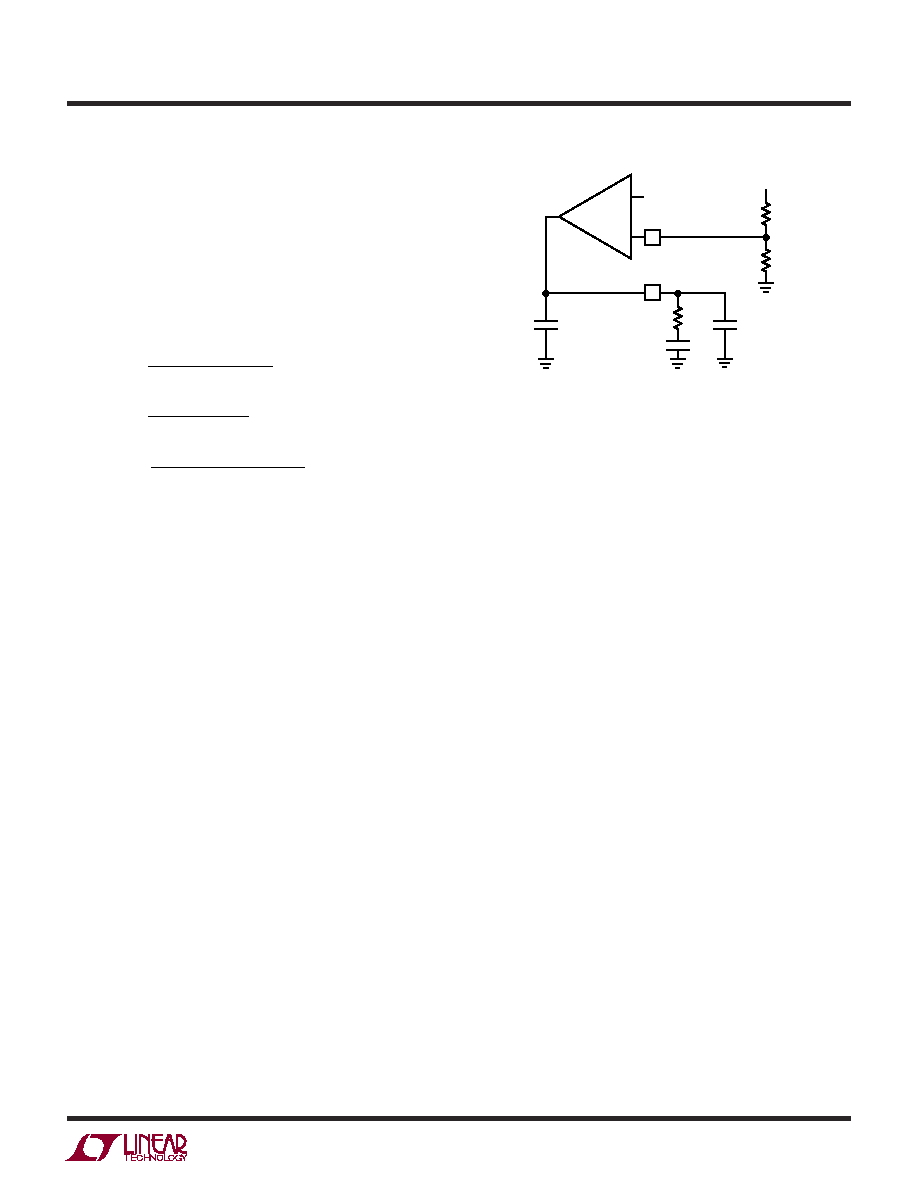
Closing the Feedback Loop
The LTC3428 uses current mode control with internal,
adaptive slope compensation. Current mode control elimi-
nates the 2nd order pole in the loop response of voltage
mode converters due to the inductor and output capacitor,
simplifying it to a single pole response. The product of the
modulator control to output DC gain and the error amp
open-loop gain equals the DC gain of the system.
G
G
G
V
V
G
V
I
G
DC
CONTROL
EA
REF
OUT
CONTROL
IN
OUT
EA
=
=
∑
∑
∑
2
100
The output filter pole is given by:
f
I
V
C
Hz
POLE
OUT
OUT
OUT
=
∑
∑
where C
OUT
is the output filter capacitor value. The output
filter zero is given by:
f
R
C
Hz
ZERO
ESR
OUT
=
1
2 ∑ ∑
∑
where R
ESR
is the output capacitor equivalent series
resistance.
A complication of the boost converter topology is the right
half plane (RHP) zero and is given by:
f
V
R
L V
Hz
RHP
IN
O
O
=
2
2
2
∑
∑ ∑ ∑
LTC3428
9
3428f
Figure 3.
≠
+
1.243V
FB
R1
R2
V
C
V
OUT
R
Z
C
C1
C
C2
3428 F03
5pF
This zero causes a gain increase with phase lag. With
heavy loads, this can occur at a relatively low frequency.
For this reason, loop gain is typically rolled off below the
RHP zero frequency.
A typical error amp compensation is shown in Figure 3 and
in the Typical Application section.
The equations for the loop dynamics are as follow:
f
e
C
f
R
C
f
R
C
pF
POLE
C
ZERO
Z
C
ZERO
Z
C
1
1
1
1
2
2
1
2
400 6
1
2
1
2
5
+
∑ ∑
∑
∑ ∑
∑
∑ ∑
∑ (
)
APPLICATIO S I FOR ATIO
W
U
U
U
LTC3428
10
3428f
V
IN
SHDN
V
C
AGND
PGNDA
V
OUT
SWA
SWB
FB
PGNDB
8
4
5
7
1
3
2
9
6
10
22pF
4.7µF
10k
1000pF
4.7µF***
4◊
2.5V
IN
SHUTDOWN
4.7µH*
4.7µH*
**
**
V
OUT
3.3V, 2.5A
205k
121k
TOKO DC53LC
MICROSEMI UPS120E
TAIYO YUDEN X5R JMK212BJ475MD
*
**
***
3428 TA03
LTC3428
2.5V to 3.3V at 2.5A Converter
TYPICAL APPLICATIO S
U
LTC3428
11
3428f
U
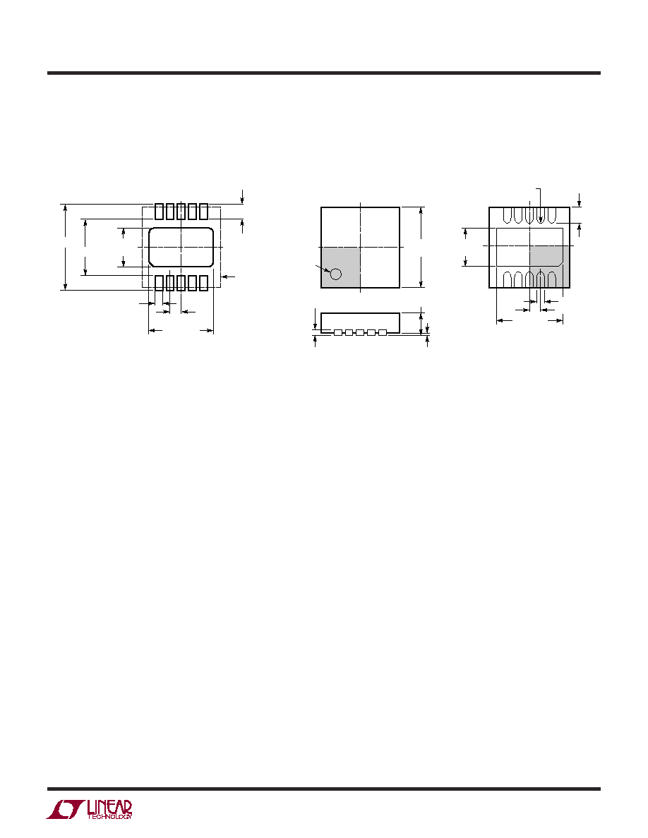
PACKAGE DESCRIPTIO
DD Package
10-Lead Plastic DFN (3mm ◊ 3mm)
(Reference LTC DWG # 05-08-1699)
Information furnished by Linear Technology Corporation is believed to be accurate and reliable.
However, no responsibility is assumed for its use. Linear Technology Corporation makes no represen-
tation that the interconnection of its circuits as described herein will not infringe on existing patent rights.
3.00 ±0.10
(4 SIDES)
NOTE:
1. DRAWING TO BE MADE A JEDEC PACKAGE OUTLINE M0-229 VARIATION OF (WEED-2).
CHECK THE LTC WEBSITE DATA SHEET FOR CURRENT STATUS OF VARIATION ASSIGNMENT
2. DRAWING NOT TO SCALE
3. ALL DIMENSIONS ARE IN MILLIMETERS
4. DIMENSIONS OF EXPOSED PAD ON BOTTOM OF PACKAGE DO NOT INCLUDE
MOLD FLASH. MOLD FLASH, IF PRESENT, SHALL NOT EXCEED 0.15mm ON ANY SIDE
5. EXPOSED PAD SHALL BE SOLDER PLATED
6. SHADED AREA IS ONLY A REFERENCE FOR PIN 1 LOCATION ON THE
TOP AND BOTTOM OF PACKAGE
0.38 ± 0.10
BOTTOM VIEW--EXPOSED PAD
1.65 ± 0.10
(2 SIDES)
0.75 ±0.05
R = 0.115
TYP
2.38 ±0.10
(2 SIDES)
1
5
10
6
PIN 1
TOP MARK
(SEE NOTE 6)
0.200 REF
0.00 ≠ 0.05
(DD10) DFN 1103
0.25 ± 0.05
2.38 ±0.05
(2 SIDES)
RECOMMENDED SOLDER PAD PITCH AND DIMENSIONS
1.65 ±0.05
(2 SIDES)
2.15 ±0.05
0.50
BSC
0.675 ±0.05
3.50 ±0.05
PACKAGE
OUTLINE
0.25 ± 0.05
0.50 BSC
LTC3428
12
3428f
Linear Technology Corporation
1630 McCarthy Blvd., Milpitas, CA 95035-7417
(408) 432-1900
FAX: (408) 434-0507
www.linear.com
© LINEAR TECHNOLOGY CORPORATION 2004
LT/TP 0804 1K ∑ PRINTED IN USA
RELATED PARTS
PART NUMBER
DESCRIPTION
COMMENTS
LT1613
550mA (I
SW
), 1.4MHz, High Efficiency Step-Up
90% Efficiency, V
IN
: 0.9V to 10V, V
OUT(MAX)
= 34V, I
Q
= 3mA,
DC/DC Converter
I
SD
<1µA, ThinSOT Package
LT1615/LT1615-1
300mA/80mA (I
SW
), High Efficiency Step-Up
V
IN
: 1V to 15V, V
OUT(MAX)
= 34V, I
Q
= 20µA,
DC/DC Converters
I
SD
<1µA, ThinSOT Package
LT1618
1.5A (I
SW
), 1.25MHz, High Efficiency Step-Up
90% Efficiency, V
IN
: 1.6V to 18V, V
OUT(MAX)
= 35V, I
Q
= 1.8mA,
DC/DC Converter
I
SD
<1µA, MS Package
LT1930/LT1930A
1A (I
SW
), 1.2MHz/2.2MHz, High Efficiency Step-Up
High Efficiency, V
IN
: 2.6V to 16V, V
OUT(MAX)
= 34V,
DC/DC Converters
I
Q
= 4.2mA/5.5mA, I
SD
<1µA, ThinSOT Package
LT1946/LT1946A
1.5A (I
SW
), 1.2MHz/2.7MHz, High Efficiency Step-Up
High Efficiency, V
IN
: 2.45V to 16V, V
OUT(MAX)
= 34V, I
Q
= 3.2mA,
DC/DC Converters
I
SD
<1µA, MS8 Package
LT1961
1.5A (I
SW
), 1.25MHz, High Efficiency Step-Up
90% Efficiency, V
IN
: 3V to 25V, V
OUT(MAX)
= 35V, I
Q
= 0.9mA,
DC/DC Converter
I
SD
6µA, MS8E Package
LTC3400/LTC3400B
600mA (I
SW
), 1.2MHz, Synchronous Step-Up
92% Efficiency, V
IN
: 0.85V to 5V, V
OUT(MAX)
= 5V, I
Q
= 19µA/300µA,
DC/DC Converter
I
SD
<1µA, ThinSOT Package
LTC3401
1A (I
SW
), 3MHz, Synchronous Step-Up DC/DC Converter
97% Efficiency, V
IN
: 0.5V to 5V, V
OUT(MAX)
= 5.5V, I
Q
= 38µA,
I
SD
<1µA, MS Package
LTC3402
2A (I
SW
), 3MHz, Synchronous Step-Up DC/DC Converter
97% Efficiency, V
IN
: 0.5V to 5V, V
OUT(MAX)
= 5.5V, I
Q
= 38µA,
I
SD
<1µA, MS Package
LTC3421
3A, 3MHz Synchronous Boost Converter
96% Efficiency, V
IN
: 0.5V to 4.5V, V
OUT(MAX)
= 5.5V, I
Q
= 12µA,
with Output Disconnect
I
SD
<1µA, QFN-24 Package
LTC3425
5A (I
SW
), 8MHz, 4-Phase Synchronous Step-Up
95% Efficiency, V
IN
: 0.5V to 4.5V, V
OUT(MAX)
= 5.25V, I
Q
= 12µA,
DC/DC Converter
I
SD
<1µA, QFN-32 Package
LTC3429
600mA, 500kHz Synchronous Boost Converter
96% Efficiency, V
IN
: 0.5V to 4.4V, V
OUT(MAX)
= 5.5V, I
Q
= 20µA,
with Output Disconnect
I
SD
<1µA, ThinSOT Package
LTC3436
3A (I
SW
), 1MHz, 34V Step-Up DC/DC Converter
V
IN
: 3V to 25V, V
OUT(MAX)
= 34V, I
Q
= 0.9mA,
I
SD
<6µA, TSSOP-16E Package
LTC3459
10V Micropower Synchronous Boost Converter
85% Efficiency, V
IN
: 1.5V to 5.5V, V
OUT(MAX)
= 10V, I
Q
= 10µA,
I
SD
<1µA, ThinSOT Package
LT3464
85mA (I
SW
), High Efficiency Step-Up DC/DC Converter
V
IN
: 2.3V to 10V, V
OUT(MAX)
= 34V, I
Q
= 25µA,
with Integrated Schottky and PNP Disconnect
I
SD
<1µA, ThinSOT Package
No R
SENSE
is a registered trademark of Linear Technology Corporation.