LTC3407
1
3407i
Information furnished by Linear Technology Corporation is believed to be accurate and reliable.
However, no responsibility is assumed for its use. Linear Technology Corporation makes no represen-
tation that the interconnection of its circuits as described herein will not infringe on existing patent rights.
Final Electrical Specifications
s
PDAs/Palmtop PCs
s
Digital Cameras
s
Cellular Phones
s
Portable Media Players
s
PC Cards
s
Wireless and DSL Modems
s
High Efficiency: Up to 96%
s
Very Low Quiescent Current: Only 40
µ
A
s
1.5MHz Constant Frequency Operation
s
High Switch Current: 1A on Each Channel
s
No Schottky Diodes Required
s
Low R
DS(ON)
Internal Switches: 0.35
s
Current Mode Operation for Excellent Line
and Load Transient Response
s
Short-Circuit Protected
s
Low Dropout Operation: 100% Duty Cycle
s
Ultralow Shutdown Current: I
Q
< 1
µ
A
s
Output Voltages from 5V down to 0.6V
s
Power-On Reset Output
s
Externally Sychronizable Oscillator
s
Small Thermally Enhanced MSOP Package
APPLICATIO S
U
FEATURES
DESCRIPTIO
U
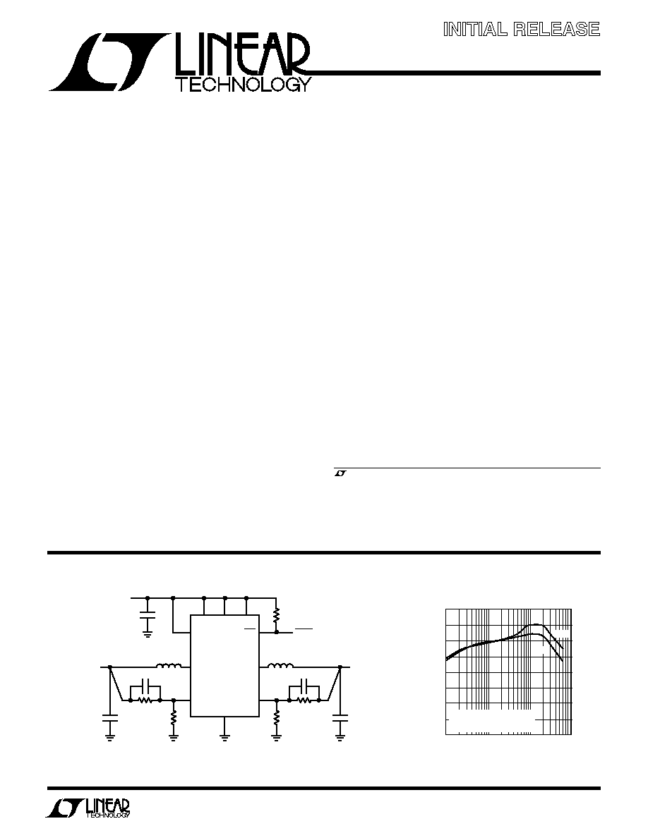
TYPICAL APPLICATIO
U
Dual Synchronous, 600mA,
1.5MHz Step-Down
DC/DC Regulator
July 2003
The LTC
Æ
3407 is a dual constant frequency, synchronous
step down DC/DC converter. Intended for low power
applications, it operates from 2.5V to 5.5V input voltage
range and has a constant 1.5MHz switching frequency,
allowing the use of tiny, low cost capacitors and inductors
2mm or less in height. Each output voltage is adjustable
from 0.6V to 5V. Internal synchronous 0.35
, 1A power
switches provide high efficiency without the need for an
external Schottky diodes.
A user selectable mode input is provided to allow the user
to trade-off ripple noise for low power efficiency. Burst
Mode
Æ
operation provides high efficiency at light loads,
while Pulse Skip Mode provides low ripple noise at light
loads.
To further maximize battery life, the P-channel MOSFETs
are turned on continously in dropout (100% duty cycle)
and both channels draw a total quiescent current of only
40
µ
A. In shutdown, the device draws <1
µ
A.
, LTC and LT are registered trademarks of Linear Technology Corporation.
Burst Mode is registered trademark of Linear Technology Corporation.
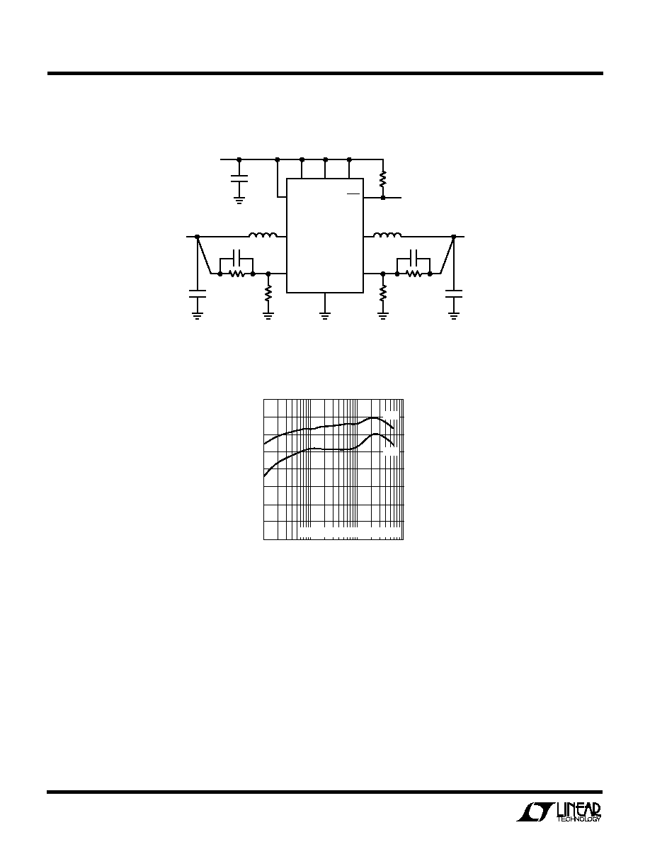
LTC3407 Efficiency Curve
Figure 1. 2.5V/1.8V at 600mA Step-Down Regulators
RUN2
V
IN
V
IN
= 2.5V
TO 5.5V
V
OUT2
= 2.5V
AT 600mA
V
OUT1
= 1.8V
AT 600mA
RUN1
POR
SW1
V
FB1
GND
V
FB2
SW2
MODE/SYNC
LTC3407
C1
10
µ
F
R5
100k
RESET
C4, 22pF
C5, 22pF
L1
2.2
µ
H
L2
2.2
µ
H
R4
887k
R2
887k
R1
443.5k
R3
280k
C3
10
µ
F
C2
10
µ
F
3407 TA01
C1, C2, C3: TAIYO YUDEN JMK316BJ106ML L1, L2: MURATA LQH32CN2R2M33
LOAD CURRENT (mA)
1
EFFICIENCY (%)
100
95
90
85
80
75
70
65
60
10
100
1000
3407 TA02
V
IN
= 3.3V
Burst Mode OPERATION
NO LOAD ON OTHER CHANNEL
2.5V
1.8V

LTC3407
2
3407i
V
IN
Voltages.................................................≠ 0.3V to 6V
V
FB1
, V
FB2
, RUN1, RUN2
Voltages ..................................... ≠ 0.3V to V
IN
+ 0.3V
MODE/SYNC Voltage ...................... ≠ 0.3V to V
IN
+ 0.3V
SW1, SW2 Voltage ......................... ≠ 0.3V to V
IN
+ 0.3V
POR Voltage ................................................≠ 0.3V to 6V
Operating Temperature Range (Note 2) .. ≠ 40
∞
C to 85
∞
C
Junction Temperature (Note 5) ............................. 125
∞
C
Storage Temperature Range ................. ≠ 65
∞
C to 150
∞
C
Lead Temperature (Soldering, 10 sec).................. 300
∞
C
ORDER PART
NUMBER
MSE PART MARKING
T
JMAX
= 125
∞
C,
JA
= 45
∞
C/W,
JC
= 10
∞
C/W
LTABA
LTC3407EMSE
ABSOLUTE AXI U
RATI GS
W
W
W
U
PACKAGE/ORDER I FOR ATIO
U
U
W
(Note 1)
ELECTRICAL CHARACTERISTICS
Note 1: Absolute Maximum Ratings are those values beyond which the life
of a device may be impaired.
Note 2: The LTC3407E is guaranteed to meet specified performance from
0
∞
C to 70
∞
C. Specifications over the ≠ 40
∞
C and 85
∞
C operating
temperature range are assured by design, characterization and correlation
with statistical process controls.
The
q
denotes the specifications which apply over the full operating
temperature range, otherwise specifications are at T
A
= 25
∞
C. V
IN
= 3.6V, unless otherwise specified. (Note 2)
SYMBOL
PARAMETER
CONDITIONS
MIN
TYP
MAX
UNITS
V
IN
Operating Voltage Range
q
2.5
5.5
V
I
FB
Feedback Pin Input Current
q
30
nA
V
FB
Feedback Voltage (Note 3)
0
∞
C
T
A
85
∞
C
0.588
0.6
0.612
V
≠40
∞
C
T
A
85
∞
C
q
0.585
0.6
0.612
V
V
LINE REG
Reference Voltage Line Regulation
V
IN
= 2.5V to 5.5V (Note 3)
0.3
0.5
%/V
V
LOAD REG
Output Voltage Load Regulation
(Note 3)
0.5
%
I
S
Input DC Supply Current
Active Mode
V
FB1
= V
FB2
= 0.5V
600
800
µ
A
Sleep Mode
V
FB1
= V
FB2
= 0.63V, MODE/SYNC = 3.6V
40
60
µ
A
Shutdown
RUN = 0V, V
IN
= 5.5V
0.1
1
µ
A
f
OSC
Oscillator Frequency
V
FB
= 0.6V
q
1.2
1.5
1.8
MHz
f
SYNC
Synchronization Frequency
1.5
MHz
I
LIM
Peak Switch Current Limit
V
IN
= 3V, FBK = 0.5V, Duty Cycle <35%
0.75
1
1.25
A
R
DS(ON)
Top Switch On-Resistance
V
IN
= 3.6V
0.35
0.45
Bottom Switch On-Resistance
V
IN
= 3.6V
0.30
0.45
I
SW(LKG)
Switch Leakage Current
V
IN
= 5V, V
RUN
= 0V, V
FB
= 0V
0.01
1
µ
A
POR
Power-On Reset Threshold
V
FB
Ramping Up, MODE/SYNC = 0V
8.5
%
V
FB
Ramping Down, MODE/SYNC = 0V
≠8.5
%
Power-On Reset On-Resistance
100
200
Power-On Reset Delay
262,144
Cycles
V
RUN
RUN Threshold High
q
0.3
1
1.5
V
I
RUN
RUN Leakage Current
q
0.01
1
µ
A
Consult LTC Marketing for parts specified with wider operating temperature ranges.
1
2
3
4
5
V
FB1
RUN1
V
IN
SW1
GND
10
9
8
7
6
V
FB2
RUN2
POR
SW2
MODE/
SYNC
TOP VIEW
MSE PACKAGE
10-LEAD PLASTIC MSOP
MSE PIN 11, EXPOSED PAD: PGND
MUST BE CONNECTED TO GND
11
Note 3: The LTC3407 is tested in a proprietary test mode that connects
FBK to the output of the error amplifier.
Note 4: Dynamic supply current is higher due to the internal gate charge
being delivered at the switching frequency.
Note 5: T
J
is calculated from the ambient T
A
and power dissipation P
D
according to the following formula: T
J
= T
A
+ (P
D
∑
JA
)
LTC3407
3
3407i
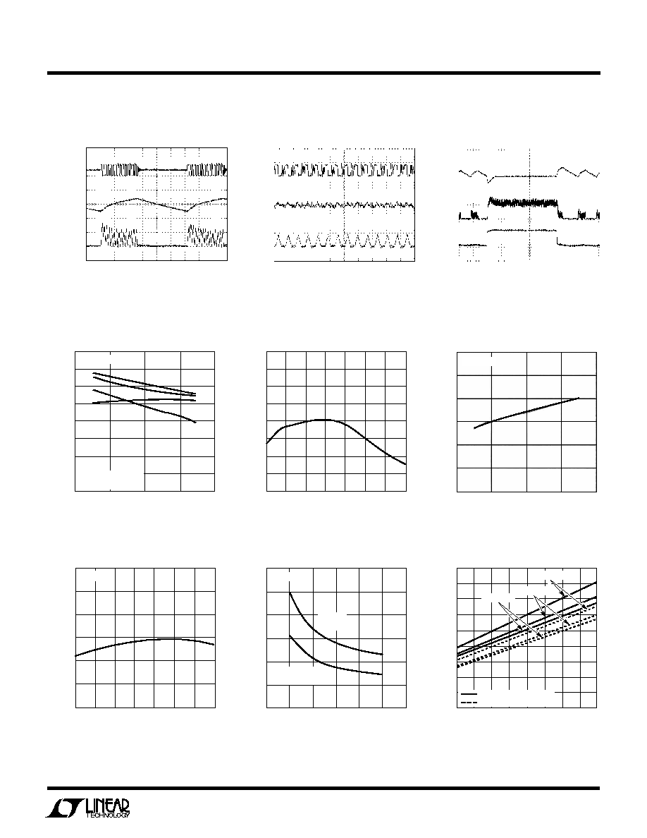
TYPICAL PERFOR A CE CHARACTERISTICS
U
W
V
IN
(V)
1
500
450
400
350
300
250
200
4
6
3407 G08
2
3
5
7
R
DS(ON)
(m
)
MAIN
SWITCH
SYNCHRONOUS
SWITCH
1.70
1.65
1.60
1.55
1.50
1.45
1.40
1.35
1.30
FREQUENCY (MHz)
0.615
0.610
0.605
0.600
0.595
0.590
0.585
REFERENCE VOLTAGE (V)
TEMPERATURE (
∞
C)
≠50
550
500
450
400
350
300
250
200
150
100
25
75
3407 G09
≠25
0
50
100
150
125
TEMPERATURE (
∞
C)
≠50
25
75
3407 G07
≠25
0
50
100
125
1.8
1.7
1.6
1.5
1.4
1.3
1.2
OSCILLATOR FREQUENCY (MHz)
SUPPLY VOLTAGE (V)
2
3407 G06
3
4
5
6
INPUT VOLTAGE (V)
2
3407 G04
3407 G01
3407 G02
3407 G03
3
4
5
6
TEMPERATURE (
∞
C)
≠50
25
75
3407 G05
≠25
0
50
100
125
R
DS(ON)
(m
)
MAIN SWITCH
SYNCHRONOUS SWITCH
V
IN
= 3.6V
100
95
90
85
80
75
70
65
60
EFFICIENCY (%)
V
IN
= 3.6V
V
IN
= 3.6V
V
OUT
= 1.8V
I
LOAD
= 50mA
CIRCUIT OF FIGURE 1
V
IN
= 3.6V
V
OUT
= 1.8V
I
LOAD
= 50mA
CIRCUIT OF FIGURE 1
V
IN
= 3.6V
V
OUT
= 1.8V
I
LOAD
= 50mA TO 600mA
CIRCUIT OF FIGURE 1
V
OUT
= 1.8V
CIRCUIT OF FIGURE 1
600mA
10mA
100mA
1mA
SW
5V/DIV
V
OUT
100mV/DIV
I
L
200mA/DIV
SW
5V/DIV
V
OUT
10mV/DIV
I
L
200mA/DIV
V
OUT
200mV/DIV
I
L
500mA/DIV
I
LOAD
500mA/DIV
4
µ
s/DIV
1
µ
s/DIV
20
µ
s/DIV
V
IN
= 4.2V
V
IN
= 2.7V
T
A
= 25
∞
C
T
A
= 25
∞
C
T
A
= 25
∞
C
Load Step
Burst Mode Operation
Pulse Skippiing Mode
Efficiency vs Input Voltage
Oscillator Frequency vs Supply
Voltage
Oscillator Frequency vs
Temperature
Reference Voltage vs
Temperature
R
DS(ON)
vs Input Voltage
R
DS(ON)
vs Temperature

LTC3407
4
3407i
LOAD CURRENT (mA)
1
EFFICIENCY (%)
100
95
90
85
80
75
70
65
60
10
100
1000
3407 G10
3.3V
2.7V
4.2V
V
OUT
= 2.5V Burst Mode OPERATION
CIRCUIT OF FIGURE 1
LOAD CURRENT (mA)
1
EFFICIENCY (%)
100
95
90
85
80
75
70
65
60
10
100
1000
3407 G13
2.7V
4.2V
V
OUT
= 1.2V Burst Mode OPERATION
CIRCUIT OF FIGURE 1
LOAD CURRENT (mA)
1
EFFICIENCY (%)
100
95
90
85
80
75
70
65
60
10
100
1000
3407 G14
2.7V
4.2V
V
OUT
= 1.5V Burst Mode OPERATION
CIRCUIT OF FIGURE 1
LOAD CURRENT (mA)
1
EFFICIENCY (%)
100
95
90
85
80
75
70
65
60
10
100
1000
3407 G11
V
IN
= 3.6V, V
OUT
= 1.8V
NO LOAD ON OTHER CHANNEL
LOAD CURRENT (mA)
1
V
OUT
ERROR (%)
4
3
2
1
0
≠1
≠2
≠3
≠4
10
100
1000
3407 G12
V
IN
= 3.6V, V
OUT
= 1.8V
NO LOAD ON OTHER CHANNEL
3.3V
V
IN
(V)
2
V
OUT
ERROR (%)
0.5
0.4
0.3
0.2
0.1
0
≠0.1
≠0.2
≠0.3
≠0.4
≠0.5
4
6
3407 G15
3
5
V
OUT
= 1.8V
I
OUT
= 200mA
T
A
= 25
∞
C
3.3V
Burst Mode OPERATION
Burst Mode OPERATION
PULSE SKIP MODE
PULSE SKIP MODE
Efficiency vs Load Current
Efficiency vs Load Current
Load Regulation
Efficiency vs Load Current
Efficiency vs Load Current
Line Regulation
TYPICAL PERFOR A CE CHARACTERISTICS
U
W

LTC3407
5
3407i
V
FB1
(Pin 1): Output Feedback. Receives the feedback
voltage from the external resistive divider across the
output. Nominal voltage for this pin is 0.6V.
RUN1 (Pin 2): Regulator 1 Enable. Forcing this pin to V
IN
enables regulator 1, while forcing it to GND causes regu-
lator 1 to shut down.
V
IN
(Pin 3): Main Power Supply. Must be closely decoupled
to GND.
SW1 (Pin 4): Regulator 1 Switch Node Connection to the
Inductor. This pin swings from V
IN
to GND.
GND (Pin 5): Main Ground. Connect to the (≠) terminal of
C
OUT
, and (≠) terminal of C
IN
.
MODE/SYNC (Pin 6): Combination Mode Selection and
Oscillator Synchronization. This pin controls the operation
of the device. When tied to V
IN
or GND, Burst Mode
operation or pulse skipping mode is selected, respec-
tively. Do not float this pin. The oscillation frequency can
U
U
U
PI FU CTIO S
be syncronized to an external oscillator applied to this pin
and pulse skipping mode is automatically selected.
SW2 (Pin 7): Regulator 2 Switch Node Connection to the
Inductor. This pin swings from V
IN
to GND.
POR (Pin 8): Power-On Reset . This common-drain logic
output is pulled to GND when the output voltage is not
within
±
8.5% of regulation and goes high after 175ms
when both channels are within regulation.
RUN2 (Pin 9): Output Feedback. Forcing this pin to V
IN
enables regulator 2, while forcing it to GND causes regu-
lator 2 to shut down.
V
FB2
(Pin 10): Output Feedback. Receives the feedback
voltage from the external resistive divider across the
output. Nominal voltage for this pin is 0.6V.
Exposed Pad (GND) (Pin 11): Power Ground. Connect to
the (≠) terminal of C
OUT
, and (≠) terminal of C
IN
. Must be
connected on PCB.
NOMINAL (V)
ABSOLUTE (V)
PIN
NAME
DESCRIPTION
MIN
TYP
MAX
MIN
MAX
1
V
FB1
Output Feedback Pin
0
0.6
V
IN
≠0.3
V
IN
+ 0.3
2
RUN1
Regulator 1 Enable
0
V
IN
≠0.3
V
IN
+ 0.3
3
V
IN
Main Power Supply
2.5
5.5
≠0.3
6
4
SW1
Regulator 1 Switch Node
0
V
IN
≠0.3
VIN + 0.3
5
GND
Main Ground
0
6
MODE/SYNC
Mode Select/Sychronizatin Pin
0
V
IN
≠0.3
V
IN
+ 0.3
7
SW2
Regulator 2 Switch Node
0
V
IN
≠0.3
V
IN
+ 0.3
8
POR
Power-On Reset Pin
0
V
IN
≠0.3
6
9
RUN2
Regulator 2 Enable
0
V
IN
≠0.3
V
IN
+ 0.3
10
V
FB2
Output Feedback Pin
0
0.6
V
IN
≠0.3
V
IN
+ 0.3
11
Exposed Pad
Power Ground for MSE Package
0

LTC3407
6
3407i
The LTC3407 uses a constant frequency, current mode
architecture. The operating frequency is set at 1.5MHz and
can be synchronized to an external oscillator. Both chan-
nels share the same clock and run in-phase. To suit a
variety of applications, the selectable Mode pin, allows the
user to trade-off noise for efficiency.
The output voltage is set by an external divider returned to
the FBK pin. An error amplfier compares the divided output
voltage with a reference voltage of 0.6V and adjusts the
peak inductor current accordingly. Overvoltage and
undervoltage comparators will pull the POR output low if
the output voltage is not within
±
8.5%. The POR output
will go high after 262,144 clock cycles (about 175ms) of
achieving regulation.
OPERATIO
U
BLOCK DIAGRA
W
1
2
9
10
8
3
4
11
5
≠
+
≠
+
≠
+
≠
+
EA
UVDET
OVDET
0.6V
7
0.65V
0.55V
≠
+
0.35V
UV
OV
I
TH
SWITCHING
LOGIC
AND
BLANKING
CIRCUIT
S
R
Q
Q
RS
LATCH
BURST
≠
+
I
COMP
I
RCMP
ANTI
SHOOT-
THRU
BURST
CLAMP
SLOPE
COMP
EN
SLEEP
POR
COUNTER
0.6V REF
OSC
OSC
REGULATOR 2 (IDENTICAL TO REGULATOR 1)
PGOOD1
PGOOD2
SHUTDOWN
V
IN
V
IN
V
IN
6
REGULATOR 1
SW1
POR
GND
SW2
5
MODE/SYNC
V
FB1
RUN1
RUN2
V
FB2
Main Control Loop
During normal operation, the top power switch (P-channel
MOSFET) is turned on at the beginning of a clock cycle
when the FBK voltage is below the the reference voltage.
The current into the inductor and the load increases until
the current limit is reached. The switch turns off and
energy stored in the inductor flows through the bottom
switch (N-channel MOSFET) into the load until the next
clock cycle.
The peak inductor current is controlled by the internally
compensated I
TH
voltage, which is the output of the error
amplifier.This amplifier compares the FBK pin to the 0.6V
reference. When the load current increases, the FBK
voltage decreases slightly below the reference. This

LTC3407
7
3407i
decrease causes the error amplifier to increase the I
TH
voltage until the average inductor current matches the new
load current.
The main control loop is shut down by pulling the RUN pin
to ground.
Low Current Operation
Two modes are available to control the operation of the
LTC3407 at low currents. Both modes automatically switch
from continuous operation to to the selected mode when
the load current is low.
To optimize efficiency, the Burst Mode operation can be
selected. When the load is relatively light, the LTC3407
automatically switches into Burst Mode operation in which
the PMOS switch operates intermittently based on load
demand with a fixed peak inductor current. By running
cycles periodically, the switching losses which are domi-
nated by the gate charge losses of the power MOSFETs are
minimized. The main control loop is interrupted when the
output voltage reaches the desired regulated value. A
hysteretic voltage comparator trips when I
TH
is below
0.28V, shutting off the switch and reducing the power. The
output capacitor and the inductor supply the power to the
load until I
TH
/RUN exceeds 0.6V, turning on the switch and
the main control loop which starts another cycle.
For lower ripple noise at low currents, the pulse skipping
mode can be used. In this mode, the LTC3407 continues
to switch at a constant frequency down to very low
currents, where it will begin skipping pulses.
Dropout Operation
When the input supply voltage decreases toward the
output voltage, the duty cycle increases to 100% which is
the dropout condition. In dropout, the PMOS switch is
turned on continuously with the output voltage being
equal to the input voltage minus the voltage drops across
the internal p-channel MOSFET and the inductor.
An important design consideration is that the R
DS(ON)
of
the P-channel switch increases with decreasing input
supply voltage (See Typical Performance Characteristics).
Therefore, the user should calculate the power dissipation
when the LTC3407 is used at 100% duty cycle with low
input voltage (See Thermal Considerations in the Applica-
tions Information Section).
Low Supply Operation
The LTC3407 incorporates an Under-Voltage Lockout
circuit which shuts down the part when the input voltage
drops below about 1.65V to prevent unstable operation.
OPERATIO
U
APPLICATIO S I FOR ATIO
W
U
U
U
A general LTC3407 application circuit is shown in
Figure 2. External component selection is driven by the
load requirement, and begins with the selection of the
inductor L. Once the inductor is chosen, C
IN
and C
OUT
can
be selected.
Inductor Selection
Although the inductor does not influence the operating
frequency, the inductor value has a direct effect on ripple
current. The inductor ripple current
I
L
decreases with
higher inductance and increases with higher V
IN
or V
OUT
:
=
I
V
f
L
V
V
L
OUT
O
OUT
IN
∑
∑
≠
1
Accepting larger values of
I
L
allows the use of low
inductances, but results in higher output voltage ripple,
greater core losses, and lower output current capability.
A reasonable starting point for setting ripple current is
I
L
= 0.3 ∑ I
LIM
, where I
LIM
is the peak switch current limit.
The largest ripple current
I
L
occurs at the maximum
input voltage. To guarantee that the ripple current stays
below a specified maximum, the inductor value should be
chosen according to the following equation:
L
V
f
I
V
V
OUT
O
L
OUT
IN MAX
=
∑
∑
≠
(
)
1
The inductor value will also have an effect on Burst Mode
operation. The transition from low current operation be-
gins when the peak inductor current falls below a level set
by the burst clamp. Lower inductor values result in higher
ripple current which causes this to occur at lower load
LTC3407
8
3407i
currents. This causes a dip in efficiency in the upper range
of low current operation. In Burst Mode operation, lower
inductance values will cause the burst frequency to in-
crease.
Inductor Core Selection
Different core materials and shapes will change the size/
current and price/current relationship of an inductor.
Toroid or shielded pot cores in ferrite or permalloy mate-
rials are small and don't radiate much energy, but gener-
ally cost more than powdered iron core inductors with
similar electrical characterisitics. The choice of which
style inductor to use often depends more on the price vs
size requirements and any radiated field/EMI require-
ments than on what the LTC3407 requires to operate.
Table 1 shows some typical surface mount inductors that
work well in LTC3407 applications.
Input Capacitor (C
IN
) Selection
In continuous mode, the input current of the converter is
a square wave with a duty cycle of approximately V
OUT
/
V
IN
. To prevent large voltage transients, a low equivalent
series resistance (ESR) input capacitor sized for the maxi-
mum RMS current must be used. The maximum RMS
capacitor current is given by:
I
I
V
V
V
V
RMS
MAX
OUT
IN
OUT
IN
(
≠
)
where the maximum average output current I
MAX
equals
the peak current minus half the peak-to-peak ripple cur-
rent, I
MAX
= I
LIM
≠
I
L
/2.
This formula has a maximum at V
IN
= 2V
OUT
, where I
RMS
= I
OUT/2
. This simple worst-case is commonly used to
design because even significant deviations do not offer
much relief. Note that capacitor manufacturer's ripple
current ratings are often based on only 2000 hours life-
time. This makes it advisable to further derate the capaci-
tor, or choose a capacitor rated at a higher temperature
than required. Several capacitors may also be paralleled to
meet the size or height requirements of the design. An
additional 0.1
µ
F to 1
µ
F ceramic capacitor is also recom-
mended on V
IN
for high frequency decoupling, when not
using an all ceramic capacitor solution.
APPLICATIO S I FOR ATIO
W
U
U
U
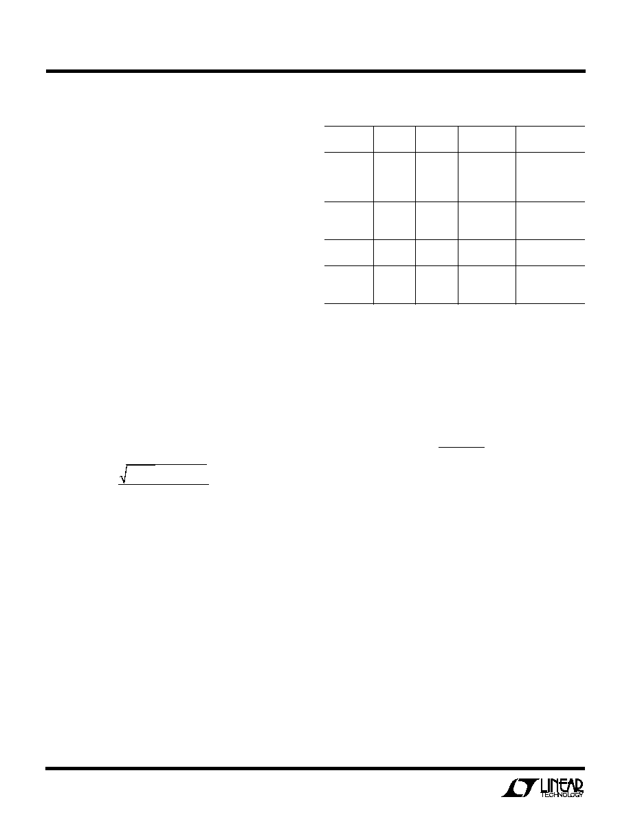
Table 1. Representative Surface Mount Inductors
PART
VALUE
DCR
MAX DC
SIZE
NUMBER
(
µ
H)
(
MAX)
CURRENT (A) W
◊
L
◊
H (mm
3
)
Sumida
1.5
0.043
1.55
3.8
◊
3.8
◊
1.8
CDRH3D16
2.2
0.075
1.20
3.3
0.110
1.10
4.7
0.162
0.90
Sumida
2.2
0.116
0.950
3.5
◊
4.3
◊
0.8
CMD4D06
3.3
0.174
0.770
4.7
0.216
0.750
Panasonic
3.3
0.17
1.00
4.5
◊
5.4
◊
1.2
ELT5KT
4.7
0.20
0.95
Murata
1.0
0.060
1.00
2.5
◊
3.2
◊
2.0
LQH32CN
2.2
0.097
0.79
4.7
0.150
0.65
Output Capacitor (C
OUT
) Selection
The selection of C
OUT
is driven by the required ESR to
minimize voltage ripple and load step transients. Typically,
once the ESR requirement is satisfied, the capacitance is
adequate for filtering. The output ripple (
V
OUT
) is deter-
mined by:
+
V
I ESR
f C
OUT
L
O
OUT
1
8
where f = operating frequency, C
OUT
= output capacitance
and
I
L
= ripple current in the inductor. The output ripple
is highest at maximum input voltage since
I
L
increases
with input voltage. With
I
L
= 0.3 ∑ I
LIM
the output ripple
will be less than 100mV at maximum V
IN
and f
O
= 1MHz
with:
ESR
COUT
< 150m
Once the ESR requirements for C
OUT
have been met, the
RMS current rating generally far exceeds the I
RIPPLE(P-P)
requirement, except for an all ceramic solution.
In surface mount applications, multiple capacitors may
have to be paralleled to meet the capacitance, ESR or RMS
current handling requirement of the application. Alumi-
num electrolytic, special polymer, ceramic and dry tantulum
capacitors are all available in surface mount packages. The
OS-CON semiconductor dielectric capacitor available from
Sanyo has the lowest ESR(size) product of any aluminum
electrolytic at a somewhat higher price. Special polymer

LTC3407
9
3407i
capacitors, such as Sanyo POSCAP, offer very low ESR,
but have a lower capacitance density than other types.
Tantalum capacitors have the highest capacitance density,
but it has a larger ESR and it is critical that the capacitors
are surge tested for use in switching power supplies. An
excellent choice is the AVX TPS series of surface mount
tantalums, available in case heights ranging from 2mm to
4mm. Aluminum electrolytic capacitors have a signifi-
cantly larger ESR, and are often used in extremely cost-
sensitive applications provided that consideration is given
to ripple current ratings and long term reliability. Ceramic
capacitors have the lowest ESR and cost, but also have the
lowest capacitance density, a high voltage and tempera-
ture coefficient, and exhibit audible piezoelectric effects.
In addition, the high Q of ceramic capacitors along with
trace inductance can lead to significant ringing. Other
capacitor types include the Panasonic Special Polymer
(SP) capacitors.
In most cases, 0.1
µ
F to 1
µ
F of ceramic capacitors should
also be placed close to the LTC3407 in parallel with the
main capacitors for high frequency decoupling.
Ceramic Input and Output Capacitors
Higher value, lower cost ceramic capacitors are now
becoming available in smaller case sizes. These are tempt-
ing for switching regulator use because of their very low
ESR. Unfortunately, the ESR is so low that it can cause
loop stability problems. Solid tantalum capacitor ESR
generates a loop "zero" at 5kHz to 50kHz that is instrumen-
tal in giving acceptable loop phase margin. Ceramic ca-
pacitors remain capacitive to beyond 300kHz and usually
resonate with their ESL before ESR becomes effective.
APPLICATIO S I FOR ATIO
W
U
U
U
Figure 2. LTC3407 General Schematic
RUN2
V
IN
V
IN
= 2.5V
TO 5.5V
V
OUT2
V
OUT1
RUN1
POR
SW1
V
FB1
GND
V
FB2
SW2
MODE/SYNC
LTC3407
C
IN
R5
POWER-ON
RESET
C4
C5
L1
L2
R4
R2
R1
R3
C
OUT2
C
OUT1
3407 F02
PS*
BM*
*MODE/SYNC = 0V: PULSE SKIP
MODE/SYNC = V
IN
: BURST MODE
Also, ceramic caps are prone to temperature effects which
requires the designer to check loop stability over the
operating temperature range. To minimize their large
temperature and voltage coefficients, only X5R or X7R
ceramic capacitors should be used. A good selection of
ceramic capacitors is available from Taiyo Yuden, TDK,
and Murata.
Great care must be taken when using only ceramic input
and output capacitors. When a ceramic capacitor is used
at the input and the power is being supplied through long
wires, such as from a wall adapter, a load step at the output
can induce ringing at the V
IN
pin. At best, this ringing can
couple to the output and be mistaken as loop instability. At
worst, the ringing at the input can be large enough to
damage the part.
Since the ESR of a ceramic capacitor is so low, the input
and output capacitor must instead fulfill a charge storage
requirement. During a load step, the output capacitor must
instantaneously supply the current to support the load
until the feedback loop raises the switch current enough to
support the load. The time required for the feedback loop
to respond is dependent on the compensation and the
output capacitor size. Typically, 3-4 cycles are required to
respond to a load step, but only in the first cycle does the
output drop linearly. The output droop, V
DROOP
, is usually
about 2-3 times the linear drop of the first cycle. Thus, a
good place to start is with the output capacitor size of
approximately:
C
I
f
V
OUT
OUT
O
DROOP
2 5
.
∑
More capacitance may be required depending on the duty
cycle and load step requirements.
In most applications, the input capacitor is merely re-
quired to supply high frequency bypassing, since the
impedance to the supply is very low. A 10
µ
F ceramic
capacitor is usually enough for these conditions.
Setting the Output Voltage
The LTC3407 develops a 0.6V reference voltage between
the feedback pin, V
FB
, and the ground as shown in
Figure 2. The output voltage is set by a resistive divider
according to the following formula:

LTC3407
10
3407i
Hot Swap is registered trademark of Linear Technology Corporation.
V
V
R
R
OUT
=
+
0 6
1
2
1
.
Keeping the current small (<5
µ
A) in these resistors maxi-
mizes efficiency, but making them too small may allow
stray capacitance to cause noise problems and reduce the
phase margin of the error amp loop.
To improve the frequency response, a feed-forward ca-
pacitor C
F
may also be used. Great care should be taken to
route the V
FB
line away from noise sources, such as the
inductor or the SW line.
Power-On Reset
The POR pin is an open-drain output which pulls low when
either regulator is out of regulation. When both output
voltages are within
±
8.5% of regulation, a timer is started
which releases POR after 2
18
clock cycles (about 175ms).
This delay can be significantly longer in Burst Mode
operation with low load currents, since the clock cycles
only occur during a burst and there could be milliseconds
of time between bursts. This can be bypassed by tying the
POR output to the MODE/SYNC input, to force pulse
skipping mode during a reset. In addition, if the output
voltage faults during Burst Mode sleep, POR could have a
slight delay for an undervoltage output condition and may
not respond to an overvoltage output. This can be avoided
by using pulse skipping mode instead. When either chan-
nel is shut down, the POR output is pulled low, since one
or both of the channels are not in regulation.
Mode Selection & Frequency Synchronization
The MODE/SYNC pin is a multipurpose pin which provides
mode selection and frequency synchronization. Connect-
ing this pin to V
IN
enables Burst Mode operation, which
provides the best low current efficiency at the cost of a
higher output voltage ripple. When this pin is connected to
ground, pulse skipping operation is selected which pro-
vides the lowest output ripple, at the cost of low current
efficiency.
The LTC3407 can also be synchronized to an external
1.5MHz clock signal by the MODE/SYNC pin. During
synchronization, the mode is set to pulse skipping and the
top switch turn-on is synchronized to the rising edge of the
external clock.
Checking Transient Response
The regulator loop response can be checked by looking at
the load transient response. Switching regulators take
several cycles to respond to a step in load current. When
a load step occurs, V
OUT
immediately shifts by an amount
equal to
I
LOAD
∑ ESR, where ESR is the effective series
resistance of C
OUT
.
I
LOAD
also begins to charge or
discharge C
OUT
generating a feedback error signal used by
the regulator to return V
OUT
to its steady-state value.
During this recovery time, V
OUT
can be monitored for
overshoot or ringing that would indicate a stability prob-
lem.
The initial output voltage step may not be within the
bandwidth of the feedback loop, so the standard second-
order overshoot/DC ratio cannot be used to determine
phase margin. In addition, a feed-forward capacitor, C
F
,
can be added to improve the high frequency response, as
shown in Figure 2. Capacitor C
F
provides phase lead by
creating a high frequency zero with R2 which improves the
phase margin.
The output voltage settling behavior is related to the
stability of the closed-loop system and will demonstrate
the actual overall supply performance. For a detailed
explanation of optimizing the compensation components,
including a review of control loop theory, refer to Applica-
tion Note 76.
In some applications, a more severe transient can be
caused by switching in loads with large (>1
µ
F) input
capacitors. The discharged input capacitors are effectively
put in parallel with C
OUT
, causing a rapid drop in V
OUT
. No
regulator can deliver enough current to prevent this prob-
lem, if the switch connecting the load has low resistance
and is driven quickly. The solution is to limit the turn-on
speed of the load switch driver. A Hot Swap
TM
controller is
designed specifically for this purpose and usually incorpo-
rates current limiting, short-circuit protection, and soft-
starting.
Efficiency Considerations
The percent efficiency of a switching regulator is equal to
the output power divided by the input power times 100%.
It is often useful to analyze individual losses to determine
what is limiting the efficiency and which change would
APPLICATIO S I FOR ATIO
W
U
U
U

LTC3407
11
3407i
produce the most improvement. Percent efficiency can be
expressed as:
%Efficiency = 100% - (L1 + L2 + L3 + ...)
where L1, L2, etc. are the individual losses as a percentage
of input power.
Although all dissipative elements in the circuit produce
losses, 4 main sources usually account for most of the
losses in LTC3407 circuits: 1)V
IN
quiescent current, 2)
switching losses, 3) I
2
R losses, 4) other losses.
1) The V
IN
current is the DC supply current given in the
Electrical Characteristics which excludes MOSFET driver
and control currents. V
IN
current results in a small (<0.1%)
loss that increases with V
IN
, even at no load.
2) The switching current is the sum of the MOSFET driver
and control currents. The MOSFET driver current results
from switching the gate capacitance of the power MOSFETs.
Each time a MOSFET gate is switched from low to high to
low again, a packet of charge dQ moves from V
IN
to
ground. The resulting dQ/dt is a current out of V
IN
that is
typically much larger than the DC bias current. In continu-
ous mode, I
GATECHG
= f
O
(Q
T
+ Q
B
), where Q
T
and Q
B
are the
gate charges of the internal top and bottom MOSFET
switches. The gate charge losses are proportional to V
IN
and thus their effects will be more pronounced at higher
supply voltages.
3) I
2
R losses are calculated from the DC resistances of the
internal switches, R
SW
, and external inductor, R
L
. In
continuous mode, the average output current flowing
through inductor L, but is "chopped" between the internal
top and bottom switches. Thus, the series resistance
looking into the SW pin is a function of both top and
bottom MOSFET R
DS(ON)
and the duty cycle (DC) as
follows:
R
SW
= (R
DS(ON)TOP
)(DC) + (R
DS(ON)BOT
)(1 ≠ DC)
The R
DS(ON)
for both the top and bottom MOSFETs can be
obtained from the Typical Performance Characteristics
curves. Thus, to obtain I
2
R losses:
I
2
R losses = I
OUT2
(R
SW
+ R
L
)
4) Other `hidden' losses such as copper trace and internal
battery resistances can account for additional efficiency
degradations in portable systems. It is very important to
include these "system" level losses in the design of a
system. The internal battery and fuse resistance losses
can be minimized by making sure that C
IN
has adequate
charge storage and very low ESR at the switching fre-
quency. Other losses including diode conduction losses
during dead-time and inductor core losses generally ac-
count for less than 2% total additional loss.
Thermal Considerations
In a majority of applications, the LTC3407 does not
dissipate much heat due to its high efficiency. However, in
applications where the LTC3407 is running at high ambi-
ent temperature with low supply voltage and high duty
cycles, such as in dropout, the heat dissipated may exceed
the maximum junction temperature of the part. If the
junction temperature reaches approximately 150
∞
C, both
power switches will be turned off and the SW node will
become high impedance.
To avoid the LTC3407 from exceeding the maximum
junction temperature, the user will need to do some
thermal analysis. The goal of the thermal analysis is to
determine whether the power dissipated exceeds the
maximum junction temperature of the part. The tempera-
ture rise is given by:
T
RISE
= P
D
∑
JA
where P
D
is the power dissipated by the regulator and
JA
is the thermal resistance from the junction of the die to the
ambient temperature.
The junction temperature, T
J
, is given by:
T
J
= T
RISE
+ T
AMBIENT
As an example, consider the case when the LTC3407 is in
dropout on both channels at an input voltage of 2.7V with
a load current of 600mA and an ambient temperature of
70
∞
C. From the Typical Performance Characteristics graph
of Switch Resistance, the R
DS(ON)
resistance of the main
switch is 0.425
. Therefore, power dissipated by each
channel is:
P
D
= I
2
∑ R
DS(ON)
= 153mW
The MS package junction-to-ambient thermal resistance,
JA
, is 45
∞
C/W. Therefore, the junction temperature of the
APPLICATIO S I FOR ATIO
W
U
U
U
LTC3407
12
3407i
Figure 3. LTC3407 Layout Diagram (See Board Layout Checklist)
RUN2
V
IN
V
IN
V
OUT2
V
OUT1
RUN1
POR
SW1
V
FB1
GND
V
FB2
SW2
MODE/SYNC
LTC3407
C
IN
C4
C5
L1
L2
R4
R2
R1
R3
C
OUT2
C
OUT1
3407 F03
BOLD LINES INDICATE HIGH CURRENT PATHS
regulator operating in a 70
∞
C ambient temperature is
approximately:
T
J
= 2 ∑ 0.153 ∑ 45 + 70 = 84
∞
C
which is below the absolute maximum junction tempera-
ture of 125
∞
C.
Design Example
As a design example, consider using the LTC3407 in an
portable application with a Li-Ion battery. The battery
provides a V
IN
= 2.8V to 4.2V. The load requires a maxi-
mum of 600mA in active mode and 2mA in standby mode.
The output voltage is V
OUT
= 2.5V. Since the load still
needs power in standby, Burst Mode operation is selected
for good low load efficiency.
First, calculate the inductor value for about 30% ripple
current at maximum V
IN
:
L
V
MHz
mA
V
V
H
=
=
µ
2 5
1 5
300
1
2 5
4 2
2 25
.
.
∑
∑
≠
.
.
.
Choosing the closest inductor from a vendor of 2.2
µ
H
inductor, results in a maximum ripple current of:
=
µ
-
=
I
V
MHz
V
V
mA
L
2 5
1 5
2 2
1
2 5
4 2
307
.
.
∑ .
∑
.
.
For cost reasons, a ceramic capacitor will be used. C
OUT
selection is then based on load step droop instead of ESR
requirements. For a 5% output droop:
C
mA
MHz
V
F
OUT
= µ
2 5
600
1 5
5
2 5
8
.
.
∑ ( %∑ .
)
The closest standard value is 10
µ
F. Since the output
impedance of a Li-Ion battery is very low, C
IN
is typically
10
µ
F.
The output voltage can now be programmed by choosing
the values of R1 and R2. To maintain high efficiency, the
current in these resistors should be kept small. Choosing
2
µ
A with the 0.6V feedback voltage makes R1~300k. A
close standard 1% resistor is 280k, and R2 is then 887k.
The PGOOD pin is a common drain output and requires a
pull-up resistor. A 100k resistor is used for adequate speed.
Figure 1 shows the complete schematic for this design
example.
Board Layout Considerations
When laying out the printed circuit board, the following
checklist should be used to ensure proper operation of the
LTC3407. These items are also illustrated graphically in
the layout diagram of Figure 3. Check the following in your
layout:
1. Does the capacitor C
IN
connect to the power V
IN
(Pin 3)
and GND (exposed pad) as close as possible? This capaci-
tor provides the AC current to the internal power MOSFETs
and their drivers.
2. Are the C
OUT
and L1 closely connected? The (≠) plate of
C
OUT
returns current to GND and the (≠) plate of C
IN
.
3. The resistor divider, R1 and R2, must be connected
between the (+) plate of C
OUT
and a ground sense line
terminated near GND (exposed pad). The feedback signals
V
FB
should be routed away from noisy components and
traces, such as the SW line (Pins 4 and 7), and its trace
should be minimized.
4. Keep sensitive components away from the SW pins. The
input capacitor C
IN
and the resistors R1 to R4 should be
routed away from the SW traces and the inductors.
5. A ground plane is preferred, but if not available, keep the
signal and power grounds segregated with small signal
components returning to the GND pin at one point and
should not share the high current path of C
IN
or C
OUT
.
6. Flood all unused areas on all layers with copper.
Flooding with copper will reduce the temperature rise of
power components. These copper areas should be con-
nected to V
IN
or GND.
APPLICATIO S I FOR ATIO
W
U
U
U

LTC3407
13
3407i
Low Ripple Buck Regulators Using Ceramic Capacitors
RUN2
V
IN
V
IN
= 2.5V
TO 5.5V
V
OUT2
= 1.8V
AT 600mA
V
OUT1
= 1.2V
AT 600mA
RUN1
POR
SW1
V
FB1
GND
V
FB2
SW2
MODE/SYNC
LTC3407
C1
10
µ
F
R5
100k
POWER-ON
RESET
C4, 22pF
C5, 22pF
L1
4.7
µ
H
L2
4.7
µ
H
R4
887k
R2
604k
R1
604k
R3
442k
C3
10
µ
F
C2
10
µ
F
3407 TA03
C1, C2, C3: TAIYO YUDEN JMK316BJ106ML L1, L2: MURATA LQH32CN4R7M11
LOAD CURRENT (mA)
1
EFFICIENCY (%)
10
100
1000
3407 TA03b
100
95
90
85
80
75
70
65
60
V
OUT
= 1.8V
V
OUT
= 1.2V
V
IN
= 3.3V Burst Mode OPERATION
LTC3407 DC568 Demo Circuit Efficiency
TYPICAL APPLICATIO S
U
LTC3407
14
3407i
TYPICAL APPLICATIO S
U
RUN2
V
IN
V
IN
= 3.6V
TO 5.5V
V
OUT2
= 3.3V
AT 600mA
V
OUT1
= 1.8V
AT 600mA
RUN1
POR
SW1
V
FB1
GND
V
FB2
SW2
MODE/SYNC
LTC3407
C1
10
µ
F
R5
100k
POWER-ON
RESET
C4, 22pF
C5, 22pF
L1
2.2
µ
H
L2
4.7
µ
H
R4
887k
R2
604k
R1
301k
R3
196k
C3
10
µ
F
C2
10
µ
F
3407 TA07
C1, C2, C3: TAIYO YUDEN JMK316BJ106ML
L1: MURATA LQH32CN2R3M33
L2: MURATA LQH32CN4R7M11
2mm Height Core Supply
Efficiency vs Load Current
LOAD CURRENT (mA)
1
EFFICIENCY (%)
100
95
90
85
80
75
70
65
60
10
100
1000
3407 TA08
3.3V
1.8V
V
IN
= 5V Burst Mode OPERATION

LTC3407
15
3407i
PACKAGE DESCRIPTIO
U
MSE Package
10-Lead Plastic MSOP
(Reference LTC DWG # 05-08-1664)
MSOP (MSE) 0603
0.53
±
0.152
(.021
±
.006)
SEATING
PLANE
0.18
(.007)
1.10
(.043)
MAX
0.17 ≠ 0.27
(.007 ≠ .011)
TYP
0.127
±
0.076
(.005
±
.003)
0.86
(.034)
REF
0.50
(.0197)
BSC
1 2 3 4 5
4.90
±
0.152
(.193
±
.006)
0.497
±
0.076
(.0196
±
.003)
REF
8
9
10
10
1
7 6
3.00
±
0.102
(.118
±
.004)
(NOTE 3)
3.00
±
0.102
(.118
±
.004)
(NOTE 4)
NOTE:
1. DIMENSIONS IN MILLIMETER/(INCH)
2. DRAWING NOT TO SCALE
3. DIMENSION DOES NOT INCLUDE MOLD FLASH, PROTRUSIONS OR GATE BURRS.
MOLD FLASH, PROTRUSIONS OR GATE BURRS SHALL NOT EXCEED 0.152mm (.006") PER SIDE
4. DIMENSION DOES NOT INCLUDE INTERLEAD FLASH OR PROTRUSIONS.
INTERLEAD FLASH OR PROTRUSIONS SHALL NOT EXCEED 0.152mm (.006") PER SIDE
5. LEAD COPLANARITY (BOTTOM OF LEADS AFTER FORMING) SHALL BE 0.102mm (.004") MAX
0.254
(.010)
0
∞
≠ 6
∞
TYP
DETAIL "A"
DETAIL "A"
GAUGE PLANE
5.23
(.206)
MIN
3.20 ≠ 3.45
(.126 ≠ .136)
0.889
±
0.127
(.035
±
.005)
RECOMMENDED SOLDER PAD LAYOUT
0.305
±
0.038
(.0120
±
.0015)
TYP
2.083
±
0.102
(.082
±
.004)
2.794
±
0.102
(.110
±
.004)
0.50
(.0197)
BSC
BOTTOM VIEW OF
EXPOSED PAD OPTION
1.83
±
0.102
(.072
±
.004)
2.06
±
0.102
(.081
±
.004)

LTC3407
16
3407i
Linear Technology Corporation
1630 McCarthy Blvd., Milpitas, CA 95035-7417
(408) 432-1900
q
FAX: (408) 434-0507
q
www.linear.com
©
LINEAR TECHNOLOGY CORPORATION 2003
RELATED PARTS
PART NUMBER
DESCRIPTION
COMMENTS
LT1616
500mA (I
OUT
), 1.4MHz,
90% Efficiency, V
IN
: 3.6V to 25V, 1.25V V
OUT(MIN)
, I
Q
= 1.9mA,
High Efficiency Step-Down DC/DC Converter
I
SD
<1
µ
A, ThinSOT Package
LTC1878
600mA (I
OUT
), 550kHz,
95% Efficiency, V
IN
: 2.7V to 6V, 0.8V V
OUT(MIN)
, I
Q
= 10
µ
A,
Synchronous Step-Down DC/DC Converter
I
SD
<1
µ
A, MSOP-8 Package
LT1940
Dual Output 1.4A(I
OUT)
, Constant 1.1MHz,
V
IN
: 3V to 25V, 1.2V V
OUT(MIN)
, I
Q
= 2.5mA, I
SD
= <1
µ
A,
High Efficiency Step-Down DC/DC Converter
TSSOP-16E Package
LTC3252
Dual 250mA (I
OUT
), 1MHz, Spread Spectrum
88% Efficiency, V
IN
: 2.7V to 5.5V, V
OUT(MIN)
: 0.9V to 1.6V, I
Q
= 60
µ
A
Inductorless Step-Down DC/DC Converter
I
SD
< 1
µ
A, DFN-12 Package
LTC3405/LTC3405A
300mA (I
OUT
), 1.5MHz,
95% Efficiency, V
IN
: 2.5V to 5.5V, 0.8V V
OUT(MIN)
, I
Q
= 20
µ
A,
Synchronous Step-Down DC/DC Converters
I
SD
<1
µ
A, ThinSOT Package
LTC3406/LTC3406B
600mA (I
OUT
), 1.5MHz,
95% Efficiency, V
IN
: 2.5V to 5.5V, 0.6V V
OUT(MIN)
, I
Q
= 20
µ
A,
Synchronous Step-Down DC/DC Converters
I
SD
<1
µ
A, ThinSOT Package
LTC3411
1.25A (I
OUT
), 4MHz,
95% Efficiency, V
IN
: 2.5V to 5.5V, 0.8V V
OUT(MIN)
, I
Q
= 60
µ
A,
Synchronous Step Down DC/DC Converter
I
SD
<1
µ
A, MSOP-10 Package
LTC3412
2.5A (I
OUT
), 4MHz,
95% Efficiency, V
IN
: 2.5V to 5.5V, 0.8V V
OUT(MIN)
, I
Q
= 60
µ
A,
Synchronous Step Down DC/DC Converter
I
SD
<1
µ
A, TSSOP-16E Package
LTC3414
4A (IOUT), 4MHz,
95% Efficiency, V
IN
: 2.25V to 5.5V, 0.8V V
OUT(MIN)
, I
Q
= 64
µ
A,
Synchronous Step Down DC/DC Converter
I
SD
<1
µ
A, TSSOP-28E Package
LTC3440
600mA (I
OUT
), 2MHz,
95% Efficiency, V
IN
: 2.5V to 5.5V, 2.5V V
OUT(MIN)
, I
Q
= 25
µ
A,
Synchronous Buck-Boost DC/DC Converter
I
SD
<1
µ
A, MSOP-10 Package
LT/TP 0703 1K ∑ PRINTED IN USA
LOAD CURRENT (mA)
1
EFFICIENCY (%)
90
80
70
60
50
40
30
10
100
1000
3407 TA05
V
OUT
= 3.3V
BURST MODE OPERATION
4.2V
2.8V
3.6V
LOAD CURRENT (mA)
1
EFFICIENCY (%)
100
95
90
85
80
75
70
65
60
10
100
1000
3407 TA06
V
OUT
= 1.8V
BURST MODE OPERATION
4.2V
2.8V
3.6V
Efficiency vs Load Current
Efficiency vs Load Current
RUN2
V
IN
V
IN
= 2.8V
TO 4.2V
V
OUT2
= 3.3V
AT 200mA
V
OUT1
= 1.8V
AT 600mA
RUN1
POR
SW1
V
FB1
GND
V
FB2
SW2
MODE/SYNC
LTC3407
C1
10
µ
F
R5
100k
POWER-ON
RESET
C4, 22pF
L1
2.2
µ
H
L2
10
µ
H
R4
887k
R2
887k
R1
442k
R3
196k
C3
10
µ
F
C6
47
µ
F
C2
10
µ
F
3407 TA04
+
M1
D1
C1, C2, C3: TAIYO YUDEN JMK316BJ106ML
C6: SANYO 6TPB47M
D1: PHILIPS PMEG2010
L1: MURATA LQH32CN2R2M33
L2: TOKO A914BYW-100M (D52LC SERIES)
M1: SILICONIX Si2302
2mm Height Lithium-Ion Single Inductor Buck-Boost Regulator and a Buck Regulator
U
TYPICAL APPLICATIO