1
LTC3408
3408f
WCDMA Cell Phone Power Amplifiers
Wireless Modems
WCDMA Transmitter Power Supply
, LTC and LT are registered trademarks of Linear Technology Corporation.
1.5MHz, 600mA
Synchronous Step-Down
Regulator with Bypass Transistor
Dynamically Adjustable Output from 0.3V to 3.5V
600mA Output Current
Internal 0.08
P-Channel MOSFET Bypass
Transistor
High Efficiency: Up to 96%
1.5MHz Constant Frequency Operation
No Schottky Diode Required
Low Dropout Operation: 100% Duty Cycle
2.5V to 5V Input Voltage Range
Shutdown Mode Draws < 1
µA Supply Current
Current Mode Operation for Excellent Line and
Load Transient Response
Overtemperature Protected
Available in 8-Lead 3mm
◊ 3mm DFN Package
The LTC
Æ
3408 is a high efficiency monolithic synchro-
nous buck regulator optimized for WCDMA power ampli-
fier applications. The output voltage can be dynamically
programmed from 0.3V to 3.5V. At V
OUT
> 3.6V an internal
0.08
bypass P-channel MOSFET connects V
OUT
directly
to V
IN
, eliminating power loss through the inductor.
The input voltage range is 2.5V to 5V making the LTC3408
ideally suited for single Li-Ion battery-powered applica-
tions. 100% duty cycle provides low dropout operation,
extending battery life in portable systems.
Switching frequency is internally set at 1.5MHz, allowing
the use of small surface mount inductors and capacitors.
The internal synchronous switch increases efficiency and
eliminates the need for an external Schottky diode.
The LTC3408 is available in a low profile (0.75mm) 8-lead
3mm
◊ 3mm DFN package.
Efficiency Power Lost vs Load Current
U.S. Patent Numbers: 5481178, 6580258, 6304066, 6127815, 6498466, 6611131
FEATURES
DESCRIPTIO
U
APPLICATIO S
U
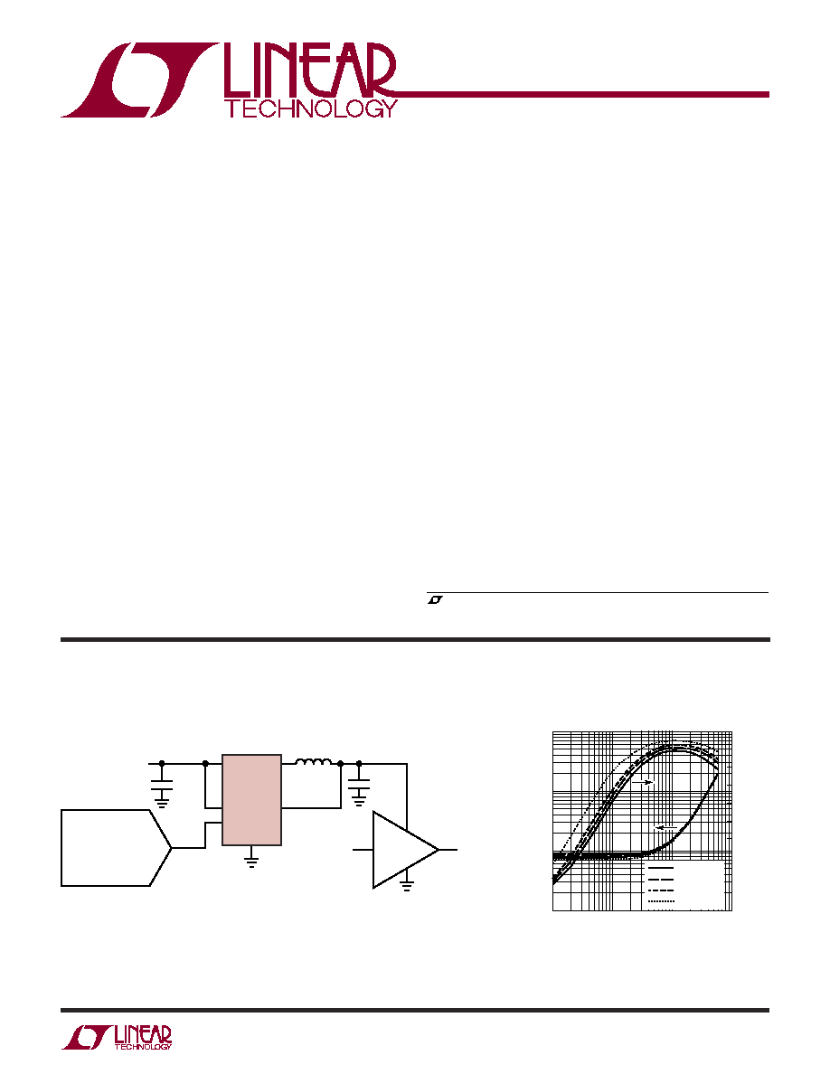
TYPICAL APPLICATIO
U
V
IN
C
IN
10
µF
CER
V
IN
2.7V
TO 5V
*
**
LTC3408
RUN
REF
4.7
µH*
3403 TA01
MURATA LQH32CN4R7M11
TAIYO YUDEN JMK212BJ475MG
TAIYO YUDEN JMK212BJ106MN
SW
V
OUT
GND
C
OUT
**
4.7
µF
CER
V
OUT
3
◊ V
REF
600mA
WCDMA
RF PA
OUTPUT
PROGRAMMING
DAC
LOAD CURRENT (mA)
1
0.01
POWER LOST (W)
EFFICIENCY (%)
0.01
0.1
1
0
20
10
60
30
70
40
80
50
90
100
10
100
1000
3408 F04
V
OUT
= 1.2V
V
OUT
= 1.5V
V
OUT
= 1.8V
V
OUT
= 2.5V
2
LTC3408
3408f
SYMBOL
PARAMETER
CONDITIONS
MIN
TYP
MAX
UNITS
V
OUT
Regulated Output Voltage
V
REF
= 1.1V
3.23
3.3
3.37
V
V
REF
= 0.1V
0.25
0.3
0.35
V
V
OUT
Output Voltage Line Regulation
V
IN
= 2.5V to 5V, V
REF
= 0.6V
0.1
0.4
%/V
I
PK
Peak Inductor Current
V
IN
= 3V, V
REF
= 0.9V
0.70
1
1.25
A
V
LOADREG
Output Voltage Load Regulation
0.7
%
V
IN
Input Voltage Range
2.5
5
V
I
S
Input Current
V
RUN
= 1.2V, SW = Open
1.5
2.5
mA
Shutdown Current
V
RUN
= 0V, SW = Open
0.1
1
µA
f
OSC
Oscillator Frequency
V
REF
0.25V
1.2
1.5
1.8
MHz
V
REF
0.1V
550
700
850
kHz
V
REF
Bypass PFET Turn-Off Threshold
V
REF
=
1.167
1.2
V
Bypass PFET Turn-On Threshold
V
REF
=
1.21
1.26
V
R
PFET
R
DS(ON)
of P-Channel FET
I
SW
= 160mA, Wafer Level
0.3
0.4
I
SW
= 160mA, DD Package
0.4
R
NFET
R
DS(ON)
of N-Channel FET
I
SW
= ≠160mA, Wafer Level
0.3
0.4
I
SW
= ≠160mA, DD Package
0.4
R
BYPASS
R
DS(ON)
of Bypass P-Channel FET
I
OUT
= 100mA, V
IN
= 3V, Wafer Level
0.05
0.08
I
OUT
= 100mA, V
IN
= 3V, DD Package (Note 4)
0.08
I
LSW
SW Leakage
V
RUN
= 0V, V
SW
= 0V or 5V, V
IN
= 5V
±0.01
±1
µA
I
LBYP
Bypass PFET Leakage
V
OUT
= 0V, V
IN
= 5V, V
REF
= 0V
±0.01
±1
µA
V
RUN
RUN Threshold
0.3
1
1.5
V
I
RUN
RUN Input Current
V
RUN
= 0V or 2.5V
±0.01
±1
µA
I
REF
REF Input Current
±0.01
±1
µA
Input Supply Voltage (< 300
µs) .................. ≠0.3V to 6V
Input Supply Voltage (DC) ....................... ≠ 0.3V to 5.5V
RUN, REF, V
OUT
Voltages .......................... ≠ 0.3V to V
IN
SW Voltage (DC) ......................... ≠ 0.3V to (V
IN
+ 0.3V)
P-Channel Switch Source Current (DC) ............. 800mA
N-Channel Switch Sink Current (DC) ................. 800mA
Peak SW Sink and Source Current ........................ 1.3A
Bypass P-Channel FET Source Current (DC) .............. 1A
Operating Temperature Range (Note 2) .. ≠ 40
∞C to 85∞C
Junction Temperature (Note 3) ............................ 125
∞C
Storage Temperature Range ................ ≠ 65
∞C to 125∞C
Consult LTC Marketing for parts specified with wider operating temperature ranges.
ABSOLUTE AXI U RATI GS
W
W
W
U
PACKAGE/ORDER I FOR ATIO
U
U
W
(Note 1)
LTC3408EDD
ORDER PART
NUMBER
DD PART MARKING
LAEA
T
JMAX
= 125
∞C,
JA
= 43
∞C/ W,
JC
= 3
∞C/ W
The
denotes specifications which apply over the full operating temperature range, otherwise specifications are T
A
= 25
∞C.
V
IN
= 3.6V unless otherwise specified.
ELECTRICAL CHARACTERISTICS
8
7
6
5
1
2
3
4
V
OUT
V
IN
REF
RUN
V
OUT
V
IN
GND
SW
TOP VIEW
DD PACKAGE
8-LEAD (3mm
◊ 3mm) PLASTIC DFN
EXPOSED PAD IS GND (PIN 9)
MUST BE SOLDERED TO PCB
9
Note 1: Absolute Maximum Ratings are those values beyond which the life
of a device may be impaired.
Note 2: The LTC3408E is guaranteed to meet performance specifications
from 0
∞C to 70∞C. Specifications over the ≠40∞C to 85∞C operating
temperature range are assured by design, characterization and correlation
with statistical process controls.
Note 3: T
J
is calculated from the ambient temperature T
A
and power
dissipation P
D
according to the following formula:
LTC3408: T
J
= T
A
+ (P
D
)(43
∞C/W)
3
LTC3408
3408f
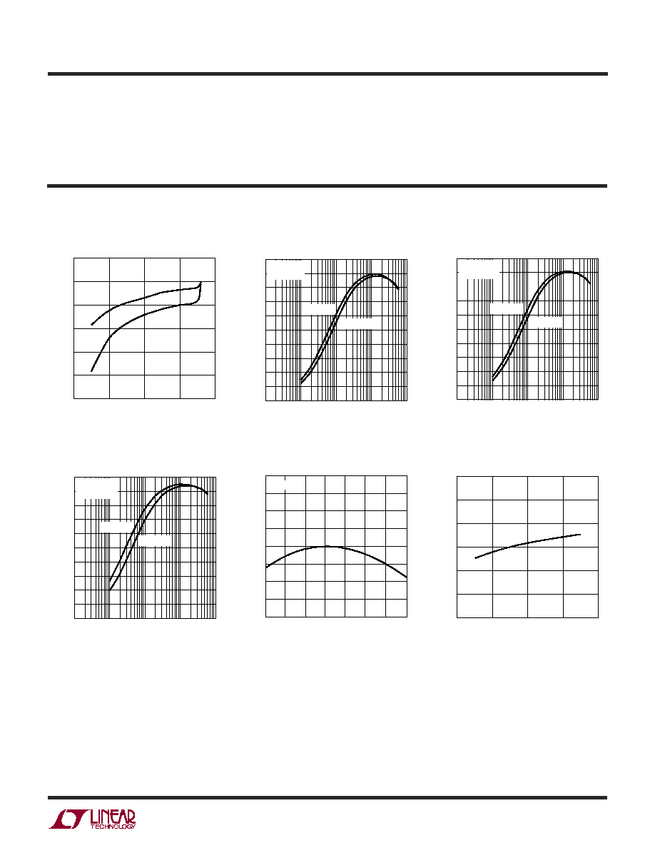
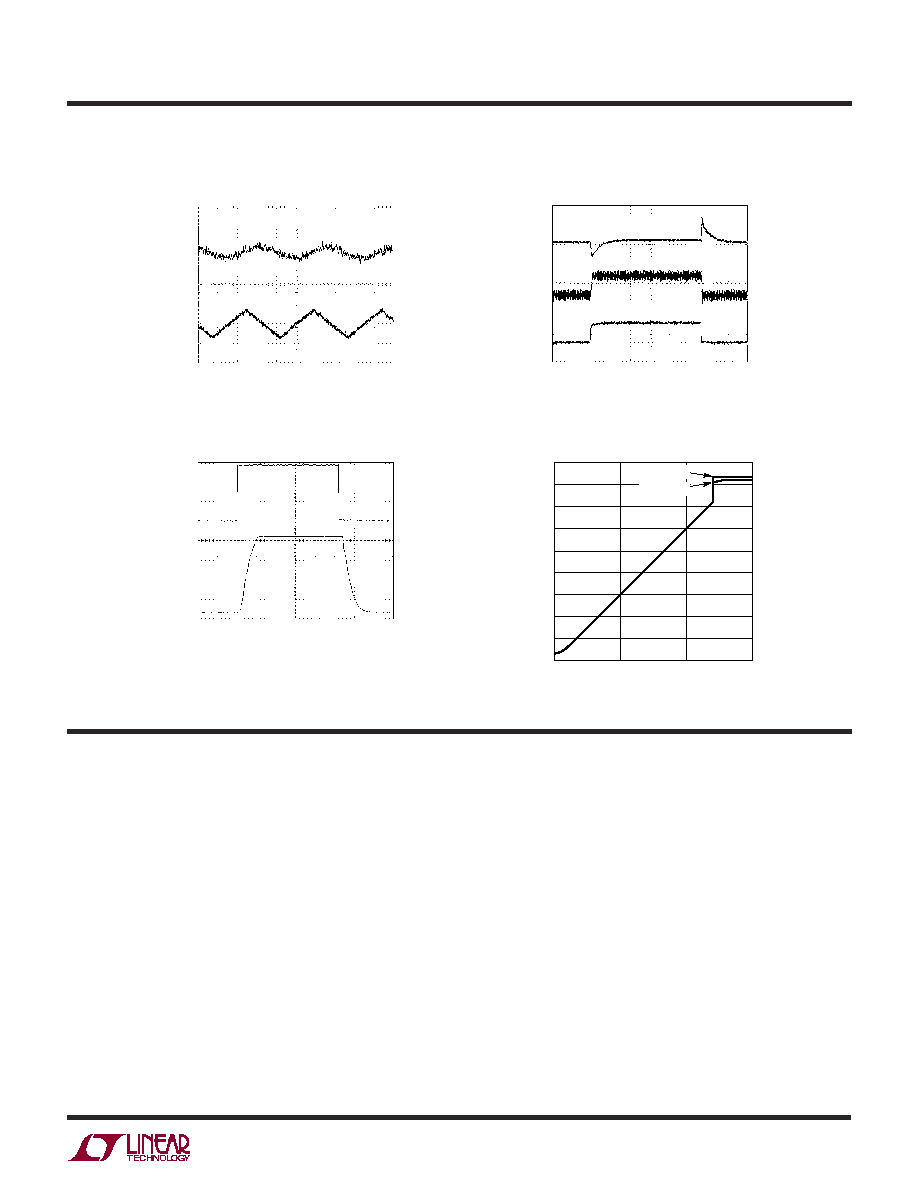
TYPICAL PERFOR A CE CHARACTERISTICS
U
W
Efficiency vs Output Current
Efficiency vs Output Current
Efficiency vs Output Current
Oscillator Frequency
vs Temperature
(From Figure 1)
ELECTRICAL CHARACTERISTICS
Efficiency vs V
OUT
Note 4: When V
REF
> 1.2V and V
REF
x3 > V
IN
, the P-channel FET will be on
in parallel with the bypass PFET reducing the overall R
DS(ON)
.
Note 5: This IC includes overtemperature protection that is intended to
protect the device during momentary overload conditions. Junction
temperature will exceed 125
∞C when overtemperature protection is active.
Continuous operation above the specified maximum operating junction
temperature may impair device reliability.
V
OUT
(V)
0
EFFICIENCY (%)
110
100
90
80
70
60
50
1
2
3
4
3408 G02
T
A
= 25
∞C
V
IN
= 3.6V
600mA
100mA
OUTPUT CURRENT (mA)
30
EFFICIENCY (%)
90
100
20
10
80
50
70
60
40
0.1
10
100
1000
3408 G03
0
1
V
IN
= 3.6V
V
IN
= 4.2V
T
A
= 25
∞C
V
OUT
= 1.2V
OUTPUT CURRENT (mA)
30
EFFICIENCY (%)
90
100
20
10
80
50
70
60
40
0.1
10
100
1000
3408 G04
0
1
V
IN
= 3.6V
V
IN
= 4.2V
T
A
= 25
∞C
V
OUT
= 1.5V
OUTPUT CURRENT (mA)
30
EFFICIENCY (%)
90
100
20
10
80
50
70
60
40
0.1
10
100
1000
3408 G05
0
1
V
IN
= 3.6V
V
IN
= 4.2V
T
A
= 25
∞C
V
OUT
= 2.5V
TEMPERATURE (
∞C)
≠50
FREQUENCY (MHz)
1.70
1.65
1.60
1.55
1.50
1.45
1.40
1.35
1.30
25
75
≠25
0
50
100
125
V
IN
= 3.6V
3408 G06
Oscillator Frequency
vs Supply Voltage
SUPPLY VOLTAGE (V)
2
OSCILLATOR FREQUENCY (MHz)
1.8
1.7
1.6
1.5
1.4
1.3
1.2
3
4
5
6
3408 G07
T
A
= 25
∞C
4
LTC3408
3408f
Output Voltage vs Load Current
R
DS(ON)
vs Input Voltage
R
DS(ON)
vs Temperature
Dynamic Supply Current
vs Supply Voltage
(From Figure 1)
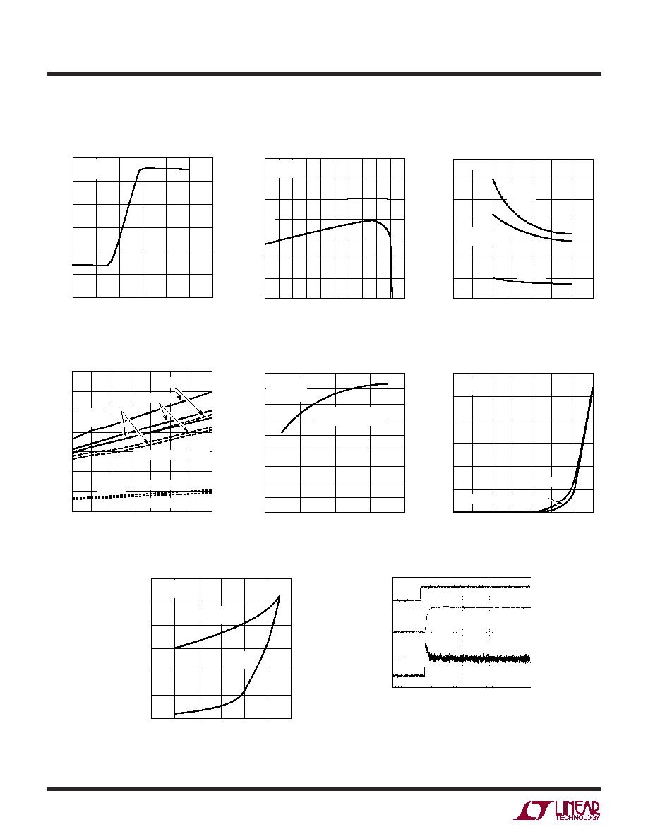
TYPICAL PERFOR A CE CHARACTERISTICS
U
W
Frequency vs V
OUT
V
OUT
(V)
0
FREQUENCY (kHz)
1600
1400
1200
1000
800
600
400
0.2
0.4
0.6
0.8
3408 G08
1.0
1.2
T
A
= 25
∞C
V
IN
= 3.6V
LOAD CURRENT (mA)
0
OUTPUT VOLTAGE (V)
1.844
1.834
1.824
1.814
1.804
1.794
1.784
1.774
100
500
700
3408 G09
400
900 1000
200 300
600
800
T
A
= 25
∞C
V
IN
= 3.6V
INPUT VOTLAGE (V)
0
0.4
0.5
0.7
3
5
3408 G10
0.3
0.2
1
2
4
6
7
0.1
0
0.6
R
DS(ON)
(
)
T
A
= 25
∞C
MAIN
SWITCH
BYPASS
SWITCH
SYNCHRONOUS
SWITCH
TEMPERATURE (
∞C)
≠50
0.4
0.5
0.7
25
75
3408 G11
0.3
0.2
≠25
0
50
100
125
0.1
0
0.6
R
DS(ON)
(
)
V
IN
= 3V
V
IN
= 4.2V
V
IN
= 4.2V
MAIN
SWITCH
BYPASS
SWITCH
SYNCHRONOUS SWITCH
V
IN
= 3.6V
V
IN
= 2.7V
SUPPLY VOLTAGE (V)
2
DYNAMIC SUPPLY CURRENT (
µ
A)
2500
3000
3500
6
3408 G12
2000
1500
0
3
4
5
1000
500
4500
4000
T
A
= 25
∞C
V
OUT
= 1.8V
I
LOAD
= 0A
FORCED CONTINUOUS
MODE
Switch Leakage vs Temperature
Switch Leakage vs Input Voltage
Start-Up from Shutdown
TEMPERATURE (
∞C)
≠50
SWITCH LEAKAGE (nA)
200
250
300
25
75
3408 G13
150
100
≠25
0
50
100
125
50
0
V
IN
= 5.5V
RUN = 0V
MAIN SWITCH
SYNCHRONOUS SWITCH
INPUT VOLTAGE (V)
0
0
SWITCH LEAKAGE (pA)
20
40
60
80
120
1
2
3
4
3408 G14
5
6
100
T
A
= 25
∞C
RUN = 0V
SYNCHRONOUS
SWITCH
MAIN
SWITCH
RUN
2V/DIV
V
OUT
1V/DIV
I
L
500mA/DIV
40
µs/DIV
V
IN
= 3.6V
V
REF
= 0.6V
R
LOAD
= 3
3408 G15
5
LTC3408
3408f
Output Ripple Waveform
Load Step Response
REF Transient
V
OUT
vs V
REF
TYPICAL PERFOR A CE CHARACTERISTICS
U
W
(From Figure 1)
V
OUT
10mV/DIV
I
L
100mA/DIV
200ns/DIV
V
IN
= 3.6V
V
REF
= 0.6V
I
LOAD
= 0A
3408 G16
V
OUT
100mV/DIV
I
L
500mA/DIV
I
LOAD
500mA/DIV
20
µs/DIV
V
IN
= 3.6V
V
REF
= 0.6V
I
LOAD
= 0mA TO 600mA
3408 G17
V
REF
(V)
0
V
OUT
(V)
1.0
4.5
4.0
3.5
3.0
2.5
2.0
1.5
1.0
0.5
0
3408 G19
0.5
1.5
V
IN
= 4.2V
I
L
= 100mA
I
L
= 600mA
U
U
U
PI FU CTIO S
V
OUT
(Pins 1, 8): Output Voltage Feedback Pin. An internal
resistive divider divides the output voltage down by 3 for
comparison to the external reference voltage. The drain of
the P-channel bypass MOSFET is connected to this pin.
V
IN
(Pins 2, 7): Main Supply Pin. Must be closely de-
coupled to GND, Pin 3, with a 10
µF or greater ceramic
capacitor.
GND (Pin 3): Ground Pin.
SW (Pin 4): Switch Node Connection to Inductor. This pin
connects to the drains of the internal main and synchro-
nous power MOSFET switches.
RUN (Pin 5): Run Control Input. Forcing this pin above
1.5V enables the part. Forcing this pin below 0.3V shuts
down the device. In shutdown, all functions are disabled
drawing <1
µA supply current. Do not leave RUN floating.
REF (Pin 6): External Reference Input. Controls the output
voltage to 3
◊ the applied voltage at REF. Also turns on the
bypass MOSFET when V
REF
> 1.2V.
Exposed Pad (Pin 9): Connect to GND, Pin 3.
V
REF
0.5V/DIV
V
OUT
1V/DIV
40
µs/DIV
V
IN
= 4.2V
V
REF
= 0V TO 1.4V
R
LOAD
= 5
3408 G18
6
LTC3408
3408f
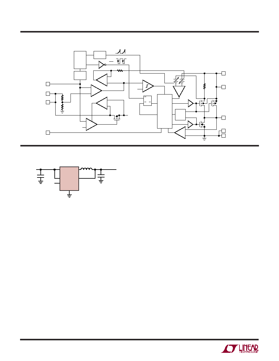
FU CTIO AL DIAGRA
U
U
W
+
≠
+
≠
+
≠
+
≠
+
≠
BCMP
EA
I
BCMP
P-CHANNEL
FB
+
≠
I
RCMP
+
≠
I
COMP
6
5
RUN
OSC
SLOPE
COMP
OSC
FREQ
˜
2
1.2V
0.85V
SLEEP
REF
8
V
OUT
1
V
OUT
360k
180k
BURST
V
IN
S
R
RS LATCH
SWITCHING
LOGIC
AND
BLANKING
CIRCUIT
ANTI-
SHOOT-
THRU
Q
Q
5
2
V
IN
7
SW
4
GND
3408 BD
3
9
V
IN
OPERATIO
U
(Refer to Functional Diagram)
Main Control Loop
The LTC3408 uses a constant frequency, current mode step-
down architecture. The main (P-channel MOSFET), syn-
chronous (N-channel MOSFET) and bypass (P-channel
MOSFET) switches are internal. During normal operation,
the internal main switch is turned on each cycle when the
oscillator sets the RS latch, and turned off when the cur-
rent comparator, I
COMP
, resets the RS latch. The peak in-
ductor current at which I
COMP
resets the RS latch, is con-
trolled by the output of error amplifier EA. When the load
current increases, it causes a slight decrease in the feed-
back voltage, FB, relative to the external reference, which
in turn, causes the EA amplifier's output voltage to increase
until the average inductor current matches the new load cur-
rent. While the main switch is off, the synchronous switch
is turned on until the beginning of the next clock cycle.
The LTC3408 operates in forced continuous mode where
the inductor current is constantly cycled. In this mode, the
output voltage can respond quickly to the external refer-
ence voltage by sourcing or sinking current as needed.
Controlling the Output Voltage
The output voltage can be dynamically programmed from
0.3V to 3.5V using the REF input. Because the gain to V
OUT
from REF is internally set to 3, the corresponding input
range at REF is 0.1V to 1.167V. V
OUT
can be modulated
during operation by driving REF with an external DAC.
When REF exceeds 1.2V, a 0.08
internal bypass P-channel
MOSFET connects V
IN
to V
OUT
, dramatically reducing the
drop across the inductor and the main switch.
Short-Circuit Protection
A current sense comparator monitors the current across
the bypass P-channel MOSFET with a trip current of about
2.5A. When this current is exceeded during a V
OUT
short
to ground, the bypass P-channel MOSFET is immediately
turned off. The propagation delay of the current sensing
comparator, I
BCMP
, detecting an overcurrent condition to
turning off the bypass P-channel MOSFET is approxmately
100ns. Once the bypass P-channel MOSFET is off for about
10
µs to 20µs, it is allowed to turn back on. The initial
current limit is then lowered to about 1.6A after the first
current limit trip. If the short to ground persists, the cur-
rent comparator will trip at the lower current limit, turning
V
IN
C
IN
10
µF
CER
V
IN
2.7V
TO 5V
LTC3408
RUN
REF
REF
4.7
µH*
3403 F01
*
**
MURATA LQH32CN4R7M11
TAIYO YUDEN JMK212BJ475MG
TAIYO YUDEN JMK212BJ106MN
SW
V
OUT
GND
C
OUT
**
4.7
µF
CER
V
OUT
3
◊ V
REF
600mA
Figure 1. Typical Application
7
LTC3408
3408f
OPERATIO
U
(Refer to Functional Diagram)
off and on the bypass P-channel MOSFET with a frequency
of approximately 50kHz to 100kHz at 1.6A peak current.
This will continue until the short is removed. While the
bypass P-channel MOSFET is pulsing intermittently, the
inherent current limit of the step-down regulator limits its
peak current to about 1A.
Dropout Operation
If the reference voltage would cause V
OUT
to exceed V
IN
,
the LTC3408 enters dropout operation. During dropout,
the main switch remains on continuously and operates at
100% duty cycle. If the voltage at REF is less than 1.2V, the
bypass P-channel MOSFET will stay off even in dropout
operation. The output voltage is then determined by the
input voltage minus the voltage drop across the main switch
and the inductor. If the voltage at REF is greater than 1.2V,
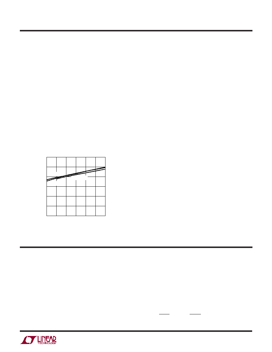
Figure 2. Maximum Output Current vs Input Voltage
SUPPLY VOLTAGE (V)
2.5
MAXIMUM OUTPUT CURRENT (mA)
1200
1000
800
600
400
200
0
3.0
3.5
4.0
4.5
3408 F02
5.0
5.5
V
OUT
= 1.8V
V
OUT
= 1.5V
V
OUT
= 2.5V
but less than V
IN
/3, the bypass P-channel MOSFET will be
on, but the main switch will be off. For best performance
and lowest voltage drop from V
IN
to V
OUT
, always ensure
that the REF voltage is greater than both 1.2V and V
IN
/3.
An important detail to remember is that at low input
supply voltages, the R
DS(ON)
of the P-channel switch
increases (see Typical Performance Characteristics).
Therefore, the user should calculate the power dissipa-
tion when the LTC3408 is used at 100% duty cycle with
low input voltage (See Thermal Considerations in the
Applications Information section).
Low Supply Operation
The LTC3408 will operate with input supply voltages as
low as 2.5V, but the maximum allowable output current is
reduced at this low voltage. Figure 2 shows the reduction
in the maximum output current as a function of input
voltage for various output voltages.
Slope Compensation and Inductor Peak Current
Slope compensation provides stability in constant fre-
quency architectures by preventing subharmonic oscilla-
tions at high duty cycles. It is accomplished internally by
adding a compensating ramp to the inductor current
signal at duty cycles in excess of 40%. Normally, this
results in a reduction of maximum inductor peak current
for duty cycles > 40%. However, the LTC3408 uses a
patent-pending scheme that counteracts this compensat-
ing ramp, which allows the maximum inductor peak
current to remain unaffected throughout all duty cycles.
APPLICATIO S I FOR ATIO
W
U
U
U
The basic LTC3408 application circuit is shown in Fig-
ure 1. External component selection is driven by the load
requirement and begins with the selection of L followed by
C
IN
and C
OUT
.
Inductor Selection
For most applications, the value of the inductor will fall in
the range of 4
µH to 6µH. Its value is chosen based on the
desired ripple current. Large value inductors lower ripple
current and small value inductors result in higher ripple
currents. As Equation 1 shows, a greater difference be-
tween V
IN
and V
OUT
produces a larger ripple current.
Where these voltages are subject to change, the highest
V
IN
and lowest V
OUT
will determine the maximum ripple
current. A reasonable starting point for setting ripple
current is I
L
= 120mA (20% of the maximum load, 600mA).
=
I
f L
V
V
V
L
OUT
OUT
IN
1
1
( )( )
≠
(1)
8
LTC3408
3408f
At output voltages below 0.6V, the switching frequency
decreases linearly to a minimum of approximately 700kHz.
This places the maximum ripple current (in forced con-
tinuous mode) at the highest input voltage and the lowest
output voltage. In practice, the resulting ouput ripple
voltage is 10mV to 15mV using the components specified
in Figure 1.
The DC current rating of the inductor should be at least equal
to the maximum load current plus half the ripple current to
prevent core saturation. Thus, a 660mA rated inductor
should be enough for most applications (600mA + 60mA).
For better efficiency, choose a low DC-resistance inductor.
Inductor Core Selection
Different core materials and shapes will change the size/
current and price/current relationship of an inductor.
Toroid or shielded pot cores in ferrite or permalloy mate-
rials are small and don't radiate much energy but generally
cost more than powdered iron core inductors with similar
electrical characteristics. The choice of which style induc-
tor to use often depends more on the price versus size
requirements and any radiated field/EMI requirements
than on what the LTC3408 requires to operate. Table 1
shows some typical surface mount inductors that work
well in LTC3408 applications.
Table 1. Representative Surface Mount Inductors
PART
VALUE
DCR
MAX DC
SIZE
NUMBER
(
µH)
(
MAX) CURRENT (A) WxLxH (mm
3
)
Sumida
4.7
0.135
0.5
3.2 x 3.2 x 1.2
CDRH2D11
Sumida
4.7
0.078
0.63
3.2 x 3.2 x 2.0
CDRH2D18/LD
Sumida
4.7
0.216
0.75
3.5 x 4.1 x 0.8
CMD4D06
Murata
4.7
0.150
0.65
2.5 x 3.2 x 2.0
LQH32C
Taiyo Yuden
4.7
0.250
0.210
1.6 x 2.0 x 1.6
LBLQ2016
Toko
4.7
0.20
0.79
3.6 x 3.6 x 1.2
D312C
C
IN
and C
OUT
Selection
In continuous mode, the source current of the top MOSFET
is a square wave of duty cycle V
OUT
/V
IN
. To prevent large
voltage transients, a low ESR input capacitor sized for the
APPLICATIO S I FOR ATIO
W
U
U
U
maximum RMS current must be used. The maximum
RMS capacitor current is given by:
C
required I
I
V
V
V
V
IN
RMS
OMAX
OUT
IN
OUT
IN
[
(
≠
)]
/
1 2
This formula has a maximum at V
IN
= 2V
OUT
, where I
RMS
= I
OUT
/2. This simple worst-case condition is commonly
used for design because even significant deviations do not
offer much relief. Note that the capacitor manufacturer's
ripple current ratings are often based on 2000 hours of life.
This makes it advisable to further derate the capacitor, or
choose a capacitor rated at a higher temperature than re-
quired. Always consult the manufacturer if there is any
question.
The selection of C
OUT
is driven by the required effective
series resistance (ESR). Typically, once the ESR
requirement for C
OUT
has been met, the RMS current
rating generally far exceeds the I
RIPPLE(P-P)
requirement.
The output ripple V
OUT
is determined by:
+
V
I ESR
f C
OUT
L
OUT
1
8
where f = operating frequency, C
OUT
= output capacitance
and I
L
= ripple current in the inductor. For a fixed output
voltage, the output ripple is highest at maximum input
voltage since I
L
increases with input voltage.
Aluminum electrolytic and dry tantalum capacitors are
both available in surface mount configurations. In the case
of tantalum, it is critical that the capacitors are surge tested
for use in switching power supplies. An excellent choice is
the AVX TPS series of surface mount tantalum. These are
specially constructed and tested for low ESR so they give
the lowest ESR for a given volume. Other capacitor types
include Sanyo POSCAP, Kemet T510 and T495 series, and
Sprague 593D and 595D series. Consult the manufacturer
for other specific recommendations.
The bulk capacitance values in Figure 1(a) (C
IN
= 10
µF,
C
OUT
= 4.7
µF) are tailored to mobile phone applications, in
which the output voltage is expected to slew quickly
according to the needs of the power amplifier. Holding the
output capacitor to 4.7
µF facilitates rapid charging and
discharging. When the output voltage descends quickly in
9
LTC3408
3408f
forced continuous mode, the LTC3408 will actually pull
current from the output until the command from V
REF
is
satisfied. On alternate half cyles, this current actually exits
the V
IN
terminal, potentially causing a rise in V
IN
and
forcing current into the battery. To prevent deterioration
of the battery, use sufficient bulk capacitance with low
ESR; at least 10
µF is recommended.
Using Ceramic Input and Output Capacitors
Higher values, lower cost ceramic capacitors are now
becoming available in smaller case sizes. Their high ripple
current, high voltage rating and low ESR make them ideal
for switching regulator applications. Because the
LTC3408's control loop does not depend on the output
capacitor's ESR for stable operation, ceramic capacitors
can be used freely to achieve very low output ripple and
small circuit size.
However, care must be taken when ceramic capacitors are
used at the input and the output. When a ceramic capacitor
is used at the input and the power is supplied by a wall
adapter through long wires, a load step at the output can
induce ringing at the input, V
IN
. At best, this ringing can
couple to the output and be mistaken as loop instability. At
worst, a sudden inrush of current through the long wires
can potentially cause a voltage spike at V
IN
large enough
to damage the part.
When choosing the input and output ceramic capacitors,
choose the X5R or X7R dielectric formulations. These
dielectrics have the best temperature and voltage charac-
teristics of all the ceramics for a given value and size.
Ceramic capacitors of Y5V material are not recommended
because normal operating voltages cause their bulk ca-
pacitance to become much less than the nominal value.
Programming the Output Voltage With a DAC
The output voltage can be dynamically programmed to any
voltage from 0.3V to 3.5V with an external DAC driving the
REF pin. When the output is commanded low, the output
voltage descends quickly in forced continuous mode
pulling current from the output and transferring it to the
input. If the input is not connected to a low impedance
source capable of absorbing the energy, the input voltage
could rise above the absolute maximum voltage of the part
and get damaged. The faster V
OUT
is commanded low, the
higher is the voltage spike at the input. For best results,
ramp the REF pin from high to low as slow as the
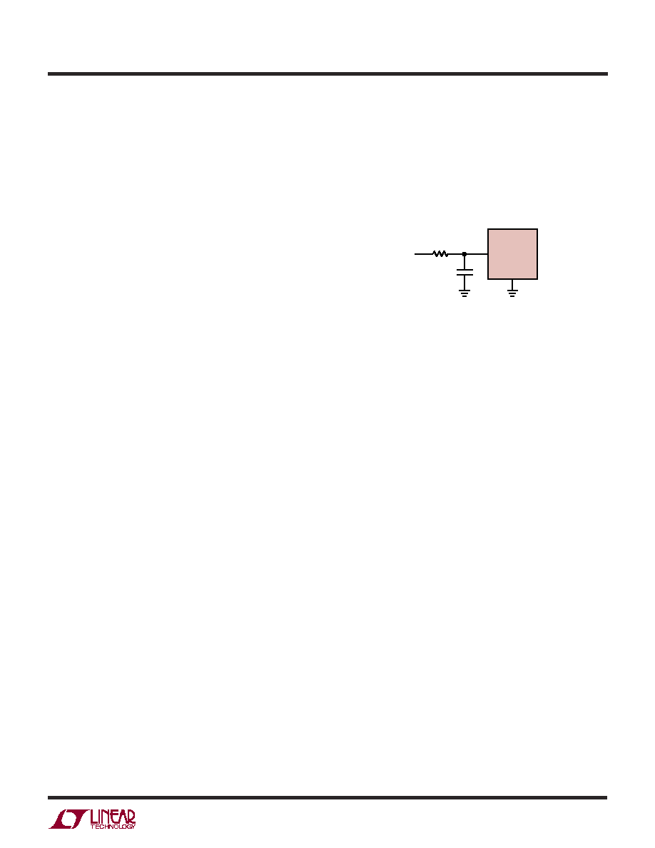
application will allow. Avoid abrupt changes in voltage of
>0.2V/
µs. If ramp control is unavailable, an RC filter with
a time constant of 10
µs can be inserted between the REF
pin and the DAC as shown in Figure 3.
APPLICATIO S I FOR ATIO
W
U
U
U
Figure 3. Filtering the REF Pin
LTC3408
REF
3408 F03
GND
DAC
10k
1000pF
Efficiency Considerations
The efficiency of a switching regulator is equal to the
output power divided by the input power times 100%. It is
often useful to analyze individual losses to determine what
is limiting the efficiency and which change would produce
the most improvement. Efficiency can be expressed as:
Efficiency = 100% ≠ (L1 + L2 + L3 + ...)
where L1, L2, etc. are the individual losses as a percentage
of input power.
Although all dissipative elements in the circuit produce
losses, two main sources usually account for most of the
losses in LTC3408 circuits: V
IN
quiescent current and I
2
R
losses. The V
IN
quiescent current loss dominates the effi-
ciency loss at low load currents whereas the I
2
R loss domi-
nates the efficiency loss at medium to high load currents.
In a typical efficiency plot, the efficiency curve at low load
currents can be misleading since the actual power lost is
of little consequence as illustrated in Figure 4.
1. The V
IN
quiescent current consists of two components:
the DC bias current as given in the electrical characteris-
tics and the internal main switch and synchronous switch
gate charge currents. The gate charge current results
from switching the gate capacitance of the internal power
MOSFET switches. Each time the gate is switched from
high to low to high again, a packet of charge, dQ, moves
from V
IN
to ground. The resulting dQ/dt is typically larger
than the DC bias current. In continuous mode,
10
LTC3408
3408f
I
GATECHG
= f(Q
T
+ Q
B
), where Q
T
and Q
B
are the gate
charges of the internal top and bottom switches. Both the
DC bias and gate charge losses are proportional to V
IN
,
thus, their effects will be more pronounced at higher
supply voltages. (The gate charge of the bypass FET is,
of course, negligible because it is infrequently cycled.)
2. I
2
R losses are calculated from the resistances of the
internal switches, R
SW
, and external inductor R
L
. In con-
tinuous mode, the average output current flowing through
inductor L is "chopped" between the main switch and the
synchronous switch. Thus, the series resistance looking
into the SW pin is a function of both top and bottom
MOSFET R
DS(ON)
and the duty cycle (DC) as follows:
R
SW
= (R
DS(ON)TOP
)(DC) + (R
DS(ON)BOT
)(1 ≠ DC)
The R
DS(ON)
for both the top and bottom MOSFETs can be
obtained from the Typical Performance Charateristics
curves. Hence, to obtain I
2
R losses, simply add R
SW
to R
L
and multiply the result by the square of the average output
current.
Other losses including C
IN
and C
OUT
ESR dissipative
losses and inductor core losses generally account for less
than 2% total additional loss.
Thermal Considerations
In most applications the LTC3408 does not dissipate
much heat due to its high efficiency. But, in applications
where the LTC3408 is running at high ambient tempera-
ture with low supply voltage and high duty cycles, such as
in dropout, the heat dissipated may exceed the maximum
junction temperature of the part. If the junction tempera-
ture reaches approximately 150
∞C, both power switches
will be turned off and the SW node will become high
impedance.
To prevent the LTC3408 from exceeding the maximum
junction temperature, the user will need to do some
thermal analysis. The goal of the thermal analysis is to
determine whether the power dissipated exceeds the
maximum junction temperature of the part. The tempera-
ture rise is given by:
T
R
= (PD)(
JA
)
where PD is the power dissipated by the regulator and
JA
is the thermal resistance from the junction of the die to the
ambient temperature.
The junction temperature, T
J
, is given by:
T
J
= T
A
+ T
R
where T
A
is the ambient temperature.
As an example, consider the LTC3408 in dropout at an
input voltage of 2.7V, a load current of 600mA (0.9V
V
REF
< 1.2V) and an ambient temperature of 70
∞C. With V
REF
<
1.2V, the entire 600mA flows through the main P-channel
FET. From the typical performance graph of switch resis-
tance, the R
DS(ON)
of the P-channel switch at 70
∞C is
approximately 0.52
. Therefore, power dissipated by the
part is:
PD = (I
LOAD
2
) ∑ R
DS(ON)
= 187.2mW
For the 8L DFN package, the
JA
is 43
∞C/W. Thus, the
junction temperature of the regulator is:
T
J
= 70
∞C + (0.1872)(43) = 78∞C
which is below the maximum junction temperature of
125
∞C.
Modifying this example, suppose that V
REF
is raised to
1.2V or higher. This turns on the bypass P-channel FET as
well as the main P-channel FET. Assume that the inductor's
DC resistance is 0.1
, the R
DS(ON)
of the main P-channel
switch is 0.52
, and the R
DS(ON)
of the bypass P-channel
switch is 0.08
. The current through the P-channel switch
and the inductor will be 69mA, causing power dissipation
of (0.069A)
2
∑ 0.62
= 2.9mW. The bypass FET will
APPLICATIO S I FOR ATIO
W
U
U
U
Figure 4. Power Lost vs Load Current
LOAD CURRENT (mA)
1
0.01
POWER LOST (W)
EFFICIENCY (%)
0.01
0.1
1
0
20
10
60
30
70
40
80
50
90
100
10
100
1000
3408 F04
V
OUT
= 1.2V
V
OUT
= 1.5V
V
OUT
= 1.8V
V
OUT
= 2.5V
11
LTC3408
3408f
dissipate (0.531A)
2
∑ 0.08
= 22.6mW. Thus, T
J
= 70
∞C +
(0.0143 + 0.0425)(43) = 71.1
∞C.
Reductions in power dissipation occur at higher supply
voltages, where the junction temperature is lower due to
reduced switch resistance (R
DS(ON)
).
Checking Transient Response
The regulator loop response can be checked by looking at
the load transient response. Switching regulators take
several cycles to respond to a step in load current. When
a load step occurs, V
OUT
immediately shifts by an amount
equal to (I
LOAD
∑ ESR), where ESR is the effective series
resistance of C
OUT
. I
LOAD
also begins to charge or dis-
charge C
OUT
, which generates a feedback error signal. The
regulator loop then acts to return V
OUT
to its steady state
value. During this recovery time V
OUT
can be monitored for
overshoot or ringing that would indicate a stability prob-
lem. For a detailed explanation of switching control loop
theory, see Application Note 76.
A second, more severe transient is caused by switching in
loads with large (>1
µF) supply bypass capacitors. The
discharged bypass capacitors are effectively put in parallel
with C
OUT
, causing a rapid drop in V
OUT
. No regulator can
deliver enough current to prevent this problem if the load
switch resistance is low and it is driven quickly. The only
solution is to limit the rise time of the switch drive so that
the load rise time is limited to approximately (25 ∑ C
LOAD
).
Thus, a 10
µF capacitor charging to 3.3V would require a
250
µs rise time, limiting the charging current to about
130mA.
APPLICATIO S I FOR ATIO
W
U
U
U
Figure 6. Suggested Layout
Figure 5. Layout Diagram
V
OUT
REF
RUN
1
2
3
4
8
7
6
5
LTC3408
3403 F05
V
IN
V
OUT
C
IN
V
OUT
SW
GND
DAC
R
REF
C
REF
C
OUT
BOLD LINES INDICATE HIGH CURRENT PATHS
V
IN
V
IN
8
7
6
5
1
2
3
4
V
OUT
V
IN
REF
RUN
V
OUT
V
IN
GND
SW
R
REF
C
REF
L1
C
OUT
C
IN
LTC3408
TO DAC
VIA TO REF
VIA TO PIN 8
VIA TO PIN 7
VIA TO GND
VIA TO PIN 1
VIA TO V
IN
3408 F06
VIA TO PIN 2
PC Board Layout Checklist
When laying out the printed circuit board, the following
checklist should be used to ensure proper operation of the
LTC3408. These items are also illustrated graphically in
Figures 5 and 6. Check the following in your layout:
1. The power traces, consisting of the GND trace, the SW
trace and the V
IN
trace should be kept short, direct and wide.
2. Does the (+) plate of C
IN
connect to V
IN
as closely as
possible? This capacitor provides the AC drive to the
internal power MOSFETs.
3. Keep the (≠) plates of C
IN
and C
OUT
as close as possible.
Design Example
As a design example, assume the LTC3408 is used in a
single lithium-ion battery-powered cellular phone applica-
tion. The V
IN
will be operating from a maximum of 4.2V
down to about 2.7V. The load current requirement is a
maximum of 0.6A but most of the time it will be in standby
mode, requiring only 2mA. Efficiency at both low and high
load currents is important. Output voltage is 2.5V. With
this information we can calculate L using Equation (1),
L
f
I
V
V
V
L
OUT
OUT
IN
=
1
1
( )(
)
≠
(2)
Information furnished by Linear Technology Corporation is believed to be accurate and reliable.
However, no responsibility is assumed for its use. Linear Technology Corporation makes no represen-
tation that the interconnection of its circuits as described herein will not infringe on existing patent rights.
12
LTC3408
3408f
Linear Technology Corporation
1630 McCarthy Blvd., Milpitas, CA 95035-7417
(408) 432-1900
FAX: (408) 434-0507
www.linear.com
LT/TP 0504 1K ∑ PRINTED IN USA
LINEAR TECHNOLOGY CORPORATION 2003
U
PACKAGE DESCRIPTIO
DD Package
8-Lead Plastic DFN (3mm
◊ 3mm)
(Reference LTC DWG # 05-08-1698)
APPLICATIO S I FOR ATIO
W
U
U
U
Figure 7
SW
V
OUT
4
1, 8
LTC3408
3403 F07
V
IN
2.7V
TO 5V
V
OUT
V
IN
RUN
REF
2, 7
5
6
GND
DAC
3, 9
C
IN
10
µF
CER
C
OUT**
4.7
µF
CER
4.7
µH*
1000pF
10k
*
**
MURATA LQH32CN4R7M11
TAIYO YUDEN JMK212BJ475MG
TAIYO YUDEN JMK212BJ106MN
Substituting V
OUT
= 2.5V, V
IN
= 4.2V, I
L
= 120mA and
f = 1.5MHz in Equation (2) gives:
L
V
MHz
mA
V
V
H
=
=
µ
2 5
1 5
120
1
2 5
4 2
5 6
.
.
(
)
≠
.
.
.
A 4.7
µH inductor works well for this application. For best
efficiency choose a 660mA or greater inductor with less
than 0.2
series resistance.
C
IN
will require an RMS current rating of at least 0.3A
LOAD(MAX)/2 at temperature and C
OUT
will require an
RELATED PARTS
PART NUMBER
DESCRIPTION
COMMENTS
LTC3403
1.5MHz, 600mA Synchronous Step-Down Regulator
Up to 96% Efficiency, V
IN
: 2.5V to 5V, V
OUT
: 0.3V to 3.5V,
with Bypass Transistor
I
Q
= 20
µA, I
SD
< 1
µA, DFN Package
LTC3405/LTC3405A-1.5/
1.5MHz, 300mA (I
OUT
) Synchronous
Up to 95% Efficiency, V
IN
: 2.5V to 5.5V, I
Q
= 20
µA,
LTC3405A-1.8
Monolithic Step-Down Regulators
Fixed Output Voltages Available, ThinSOT
TM
Package
LTC3406B/LTC3406B-1.5/ 1.5MHz, 600mA, (I
OUT
) Synchronous Monolithic
Up to 95% Efficiency, with Pulse Skipping Mode Enabled,
LTC3406B-1.8
Step-Down Regulators with Burst Mode Defeat
Fixed Output Voltages Available, ThinSOT Package
LTC3407/LTC3407-2
1.5MHz/2.25MHz, 600mA/800mA Dual (I
OUT
) Synchronous
Up to 91% Efficiency, V
IN
: 2.5V to 5.5V, I
Q
= 4
µA,
Monolithic Step-Down Regulator
MS10 Package
LTC5505
ThinSOT RF Power Detector with Buffered Output
300MHz to 3GHz, Temperatrue Compensated,
and >40dB Dynamic Range
LTC5505-1: ≠28dBm to 18dBm,
LTC5505-2: ≠32dBm to 12dBm, V
CC
= 2.7V to 6V
Burst Mode is a registered trademark of Linear Technology Corporaton. ThinSOT is a trademark of Linear Technology Corporation.
3.00
±0.10
(4 SIDES)
NOTE:
1. DRAWING TO BE MADE A JEDEC PACKAGE OUTLINE M0-229 VARIATION OF (WEED-1)
2. DRAWING NOT TO SCALE
3. ALL DIMENSIONS ARE IN MILLIMETERS
4. DIMENSIONS OF EXPOSED PAD ON BOTTOM OF PACKAGE DO NOT INCLUDE
MOLD FLASH. MOLD FLASH, IF PRESENT, SHALL NOT EXCEED 0.15mm ON ANY SIDE
0.38
± 0.10
BOTTOM VIEW--EXPOSED PAD
1.65
± 0.10
(2 SIDES)
0.75
±0.05
R = 0.115
TYP
2.38
±0.10
(2 SIDES)
1
4
8
5
PIN 1
TOP MARK
(NOTE 6)
0.200 REF
0.00 ≠ 0.05
(DD8) DFN 1203
0.25
± 0.05
2.38
±0.05
(2 SIDES)
RECOMMENDED SOLDER PAD PITCH AND DIMENSIONS
1.65
±0.05
(2 SIDES)
2.15
±0.05
0.50
BSC
0.675
±0.05
3.5
±0.05
PACKAGE
OUTLINE
0.25
± 0.05
0.50 BSC
5. EXPOSED PAD SHALL BE SOLDER PLATED
6. SHADED AREA IS ONLY A REFERENCE FOR PIN 1 LOCATION
ON TOP AND BOTTOM OF PACKAGE
ESR of less than 0.25
. In most cases, a ceramic capaci-
tor will satisfy this requirement.