1
LTC3417
3417f
PDAs/Palmtop PCs
Digital Cameras
Cellular Phones
PC Cards
Wireless and DSL Modems
Dual Synchronous
1.4A/800mA 4MHz
Step-Down DC/DC Regulator
High Efficiency: Up to 95%
1.4A/800mA Guaranteed Minimum Output Current
No Schottky Diodes Required
Programmable Frequency Operation: 1.5MHz or
Adjustable From 0.6MHz to 4MHz
Low R
DS(ON)
Internal Switches
Short-Circuit Protected
V
IN
: 2.25V to 5.5V
Current Mode Operation for Excellent Line and Load
Transient Response
125
µA Quiescent Current in Sleep Mode
Ultralow Shutdown Current: I
Q
< 1
µA
Low Dropout Operation: 100% Duty Cycle
Power Good Output
Phase Pin Selects 2nd Channel Phase Relationship
with Respect to 1st Channel
Internal Soft-Start with Individual Run Pin Control
Available in Small Thermally Enhanced
(5mm
◊ 3mm) DFN and 20-Lead TSSOP Packages
FEATURES
DESCRIPTIO
U
APPLICATIO S
U
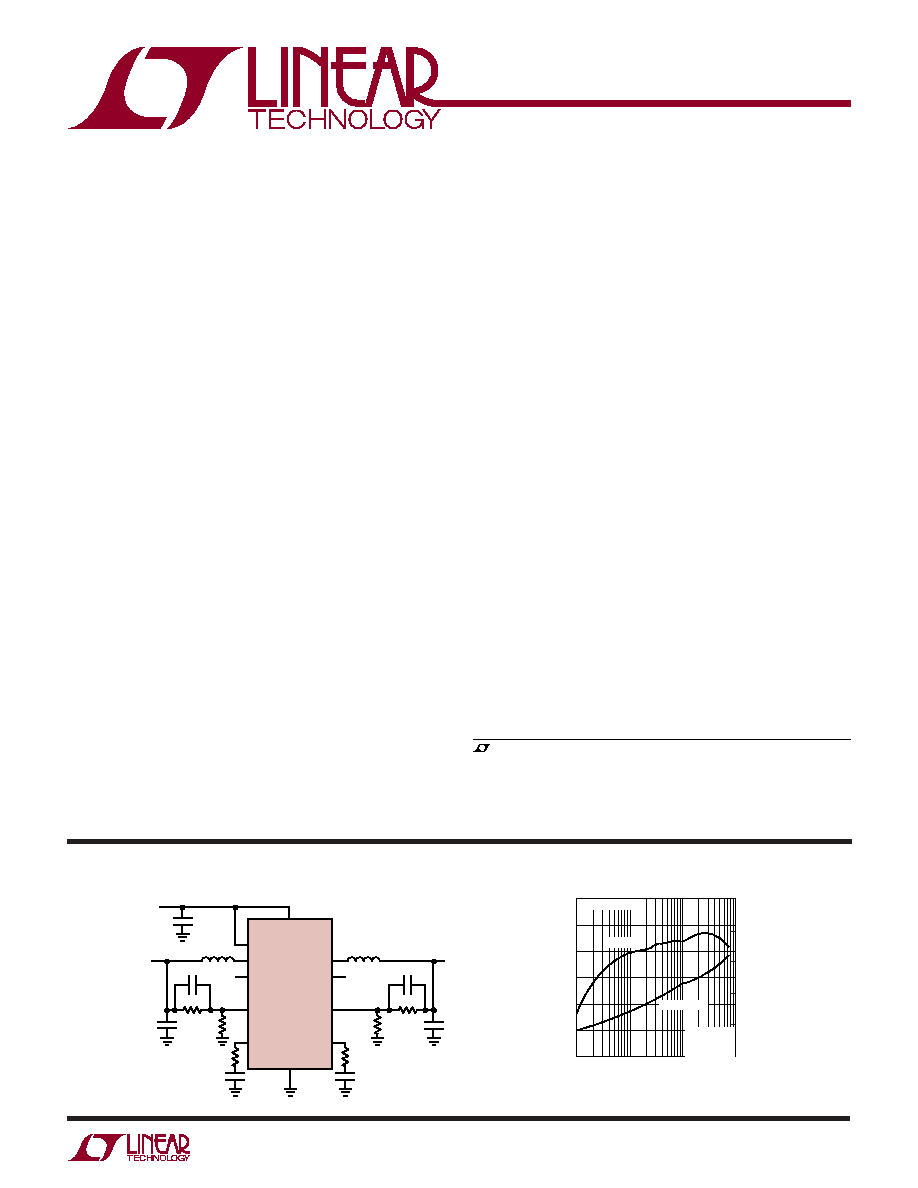
TYPICAL APPLICATIO
U
The LTC
Æ
3417 is a dual constant frequency, synchronous
step-down DC/DC converter. Intended for medium power
applications, it operates from a 2.25V to 5.5V input voltage
range and has a constant programmable switching fre-
quency, allowing the use of tiny, low cost capacitors and
inductors 2mm or less in height. Each output voltage is
adjustable from 0.8V to 5V. Internal synchronous low
R
DS(ON)
power switches provide high efficiency without
the need for external Schottky diodes.
A user selectable mode input allows the user to trade off
ripple voltage for light load efficiency. Burst Mode
Æ
opera-
tion provides high efficiency at light loads, while Pulse
Skip mode provides low ripple noise at light loads. A phase
mode pin allows the second channel to operate in-phase
or 180
∞ out-of-phase with respect to channel 1. Out-of-
phase operation produces lower RMS current on V
IN
and
thus lower RMS derating on the input capacitor.
To further maximize battery life, the P-channel MOSFETs
are turned on continuously in dropout (100% duty cycle)
and both channels draw a total quiescent current of only
100
µA. In shutdown, the device draws <1µA.
OUT2 Efficiency
(Burst Mode Operation)
, LTC and LT are registered trademarks of Linear Technology Corporation.
Burst Mode is a registered trademark of Linear Technology Corporation.
All other trademarks are the property of their respective owners.
Protected by U.S. Patents, including 5481178, 6580258, 6304066, 6127815, 6498466,
6611131, 6144194
LOAD CURRENT (A)
0.001
70
EFFICIENCY (%)
90
95
100
0.01
0.1
1
3417 TA01a
85
80
75
POWER LOSS (W)
0.001
0.01
0.1
1
10
0.0001
EFFICIENCY
REFER TO FIGURE 4
POWER LOSS
V
IN
= 3.6V
V
OUT
= 2.5V
FREQ = 1MHz
FREQ
SW1
RUN1
V
FB1
I
TH1
SW2
RUN2
V
FB2
I
TH2
V
IN
LTC3417
GND
10
µF
1.5
µH
2.2
µH
22pF
511k
22pF
866k
V
IN
V
IN
412k
412k
10
µF
5.9k
2.87k
2200pF
6800pF
3417 TA01
22
µF
V
OUT1
1.8V
1.4A
V
OUT2
2.5V
800mA
V
IN
2.5V TO 5.5V
2
LTC3417
3417f
T
JMAX
= 125
∞C,
JA
= 38
∞C/ W
EXPOSED PAD (PIN 21) IS PGND2/GNDD
MUST BE SOLDERED TO PCB
V
IN1
, V
IN2
Voltages ..................................... ≠ 0.3V to 6V
MODE, SW1, SW2, RUN1,
RUN2, V
FB1
, V
FB2
, PHASE, FREQ,
I
TH1
, I
TH2
Voltages ............. ≠ 0.3V to (V
IN1
/V
IN2
+ 0.3V)
V
IN1
≠ V
IN2
, V
IN2
≠ V
IN1
......................................... 0.3V
PGOOD Voltage .......................................... ≠ 0.3V to 6V
Consult LTC Marketing for parts specified with wider operating temperature ranges.
ABSOLUTE AXI U RATI GS
W
W
W
U
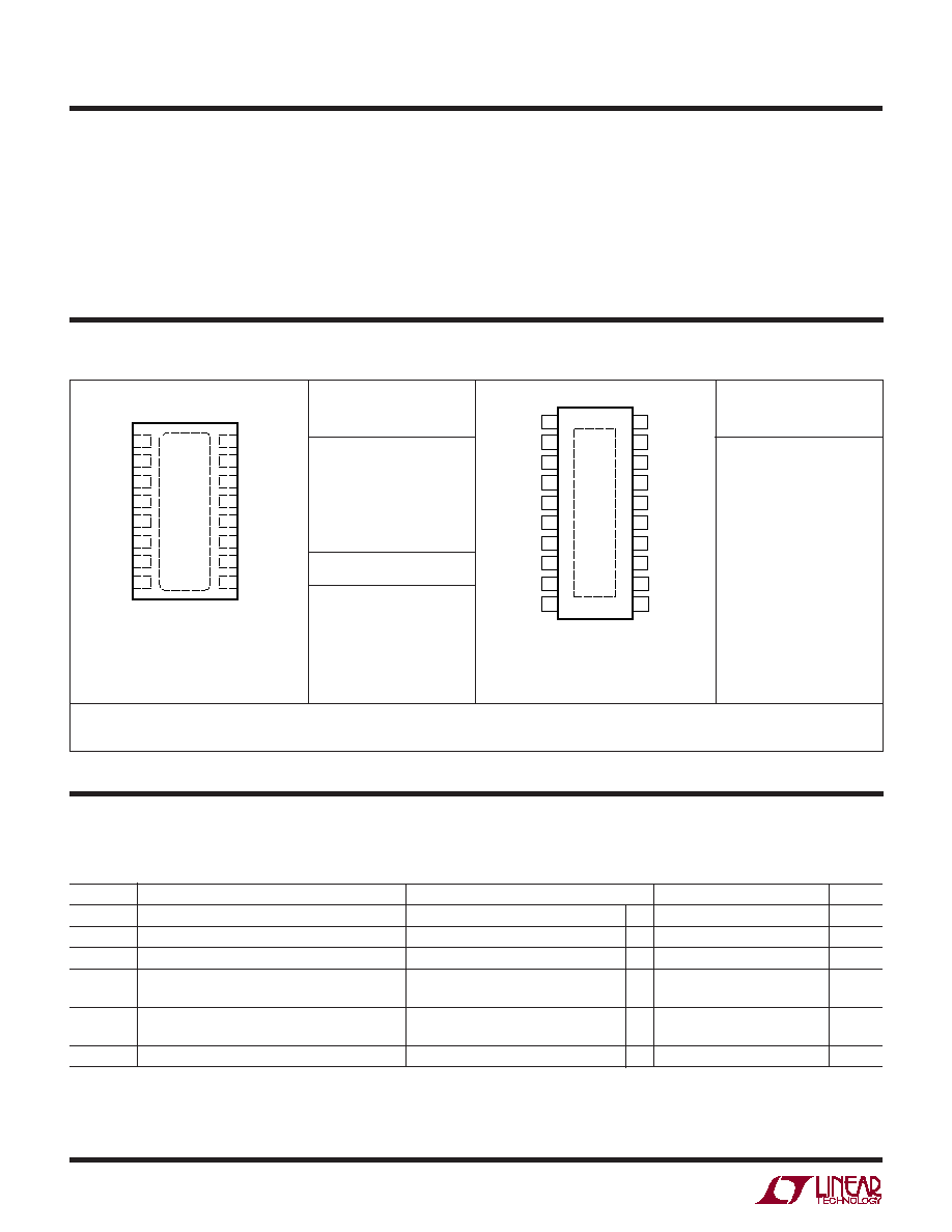
PACKAGE/ORDER I FOR ATIO
U
U
W
(Note 1)
LTC3417EDHC
ORDER PART
NUMBER
3417
T
JMAX
= 125
∞C,
JA
= 43
∞C/ W
EXPOSED PAD (PIN 17) IS PGND2/GNDD
MUST BE SOLDERED TO PCB
Operating Ambient Temperature Range
(Note 2) .................................................. ≠ 40
∞C to 85∞C
Junction Temperature (Notes 7, 8) ...................... 125
∞C
Storage Temperature Range
DFN Package ................................... ≠ 65
∞C to 125∞C
TSSOP Package ............................... ≠ 65
∞C to 150∞C
16
15
14
13
12
11
10
9
17
1
2
3
4
5
6
7
8
PGND1
SW1
PHASE
GNDA
FREQ
PGOOD
SW2
MODE
RUN1
V
IN1
ITH1
V
FB1
V
FB2
I
TH2
RUN2
V
IN2
TOP VIEW
DHC PACKAGE
16-LEAD (3mm
◊ 5mm) PLASTIC DFN
LTC3417EFE
ORDER PART
NUMBER
DHC PART MARKING
SYMBOL
PARAMETER
CONDITIONS
MIN
TYP
MAX
UNITS
V
IN1
, V
IN2
Operating Voltage Range
V
IN1
= V
IN2
2.25
5.5
V
I
FB1
, I
FB2
Feedback Pin Input Current
(Note 3)
±0.1
µA
V
FB1
, V
FB2
Feedback Voltage
(Note 3)
0.784
0.8
0.816
V
V
LINEREG
Reference Voltage Line Regulation. %/V is the
V
IN
= 2.25V to 5V (Note 3)
0.04
0.2
%/V
Percentage Change in V
OUT
with a Change in V
IN
V
LOADREG
Output Voltage Load Regulation
I
TH1
, I
TH2
= 0.36V (Note 3)
0.02
0.2
%
I
TH1
, I
TH2
= 0.84V (Note 3)
≠0.02
≠0.2
%
g
m(EA)
Error Amplifier Transconductance
I
TH1
, I
TH2(PINLOAD)
=
±5µA (Note 3)
1400
µS
The
denotes specifications which apply over the full operating temperature range, otherwise specifications are at T
A
= 25
∞C.
V
IN
= 3.6V unless otherwise specified. (Note 2)
ELECTRICAL CHARACTERISTICS
FE PACKAGE
20-LEAD PLASTIC TSSOP
1
2
3
4
5
6
7
8
9
10
TOP VIEW
20
19
18
17
16
15
14
13
12
11
GNDD
RUN1
V
IN1
I
TH1
V
FB1
V
FB2
I
TH2
RUN2
V
IN2
PGND2
GNDD
PGND1
SW1
PHASE
GNDA
FREQ
PGOOD
SW2
MODE
PGND2
21
Order Options Tape and Reel: Add #TR Lead Free: Add #PBF Lead Free Tape and Reel: Add #TRPBF
Lead Free Part Marking:
http://www.linear.com/leadfree/

3
LTC3417
3417f
SYMBOL
PARAMETER
CONDITIONS
MIN
TYP
MAX
UNITS
I
S
Input DC Supply Current (Note 4)
Active Mode
V
FB1
= V
FB2
= 0.75V, V
MODE
= V
IN
,
400
600
µA
V
RUN1
= V
RUN2
= V
IN
Half Active Mode (V
RUN2
= 0V, 1.4A Only)
V
FB1
= 0.75V, V
MODE
= V
IN
, V
RUN1
= V
IN
260
400
µA
Half Active Mode (V
RUN1
= 0V, 800mA Only) V
FB2
= 0.75V, V
MODE
= V
IN
, V
RUN2
= V
IN
260
400
µA
Both Channels in Sleep Mode
V
FB1
= V
FB2
= 1V, V
MODE
= V
IN
,
125
250
µA
V
RUN1
= V
RUN2
= V
IN
Shutdown
V
RUN1
= V
RUN2
= 0V
0.1
1
µA
f
OSC
Oscillator Frequency
V
FREQ
= V
IN
1.2
1.5
1.8
MHz
V
FREQ
: R
T
= 143k
0.85
1
1.25
MHz
V
FREQ
: Resistor (Note 6)
4
MHz
I
LIM1
Peak Switch Current Limit on SW1 (1.4A)
1.8
2.25
A
I
LIM2
Peak Switch Current Limit on SW2 (800mA)
1
1.2
A
R
DS(ON)1
SW1 Top Switch On-Resistance (1.4A)
V
IN1
= 3.6V (Note 5)
0.088
SW1 Bottom Switch On-Resistance
V
IN1
= 3.6V (Note 5)
0.084
R
DS(ON)2
SW2 Top Switch On-Resistance (800mA)
V
IN2
= 3.6V (Note 5)
0.16
SW2 Bottom Switch On-Resistance
V
IN2
= 3.6V (Note 5)
0.15
I
SW1(LKG)
Switch Leakage Current SW1 (1.4A)
V
IN1
= 6V, V
ITH1
= 0V, V
RUN1
= 0V
0.01
1
µA
I
SW2(LKG)
Switch Leakage Current SW2 (800mA)
V
IN2
= 6V, V
ITH2
= 0V, V
RUN2
= 0V
0.01
1
µA
V
UVLO
Undervoltage Lockout Threshold
V
IN1
, V
IN2
Ramping Down
1.9
2.07
2.2
V
V
IN1
, V
IN2
Ramping Up
1.95
2.12
2.25
V
T
PGOOD
Threshold for Power Good. Percentage
V
FB1
or V
FB2
Ramping Up, V
MODE
= 0V
≠6
%
Deviation from V
FB
Steady State
V
FB1
or V
FB2
Ramping Down, V
MODE
= 0V
≠6
%
(Typically 0.8V)
R
PGOOD
Power Good Pull-Down On-Resistance
160
300
V
RUN1
, V
RUN2
RUN1, RUN2 Threshold
0.3
0.85
1.5
V
V
PHASE
PHASE Threshold High-CMOS Levels
V
IN
≠0.5
V
PHASE Threshold Low-CMOS Levels
0.5
V
I
RUN1
, I
RUN2
,
RUN1, RUN2, PHASE and MODE
V
IN
= 6V, PV
IN
= 3V
0.01
1
µA
I
PHASE
, I
MODE
Leakage Current
VTL
MODE
MODE Threshold Voltage Low
0.5
V
VTH
MODE
MODE Threshold Voltage High
V
IN
≠0.5
V
VTH
FREQ
FREQ Threshold Voltage High
V
IN
≠0.5
V
The
denotes specifications which apply over the full operating temperature range, otherwise specifications are at T
A
= 25
∞C.
V
IN
= 3.6V unless otherwise specified. (Note 2)
Note 1: Absolute Maximum Ratings are those values beyond which the life
of a device may be impaired.
Note 2: The LTC3417 is guaranteed to meet specified performance from
0
∞C to 70∞C. Specifications over the ≠40∞C to 85∞C operating ambient
temperature range are assured by design, characterization and correlation
with statistical process controls.
Note 3: The LTC3417 is tested in feedback loop which servos V
FB1
to the
midpoint for the error amplifier (V
ITH1
= 0.6V) and V
FB2
to the midpoint for
the error amplifier (V
ITH2
= 0.6V).
Note 4: Total supply current is higher due to the internal gate charge being
delivered at the switching frequency.
Note 5: Switch on-resistance is guaranteed by design and test correlation
on the DHC package and by final test correlation on the FE package.
Note 6: Variable frequency operation with resistor is guaranteed by design
but not production tested and is subject to duty cycle limitations.
Note 7: This IC includes overtemperature protection that is intended to
protect the device during momentary overload conditions. Junction
temperature will exceed 125
∞C when overtemperature protection is active.
Continuous operation above the specified maximum operating junction
temperature may impair device reliability.
Note 8: T
J
is calculated from the ambient temperature, T
A
, and power
dissipation, P
D
, according to the following formula:
LTC3417EDHC: T
J
= T
A
+ (P
D
∑ 43
∞C/W)
LTC3417EFE: T
J
= T
A
+ (P
D
∑ 38
∞C/W)
ELECTRICAL CHARACTERISTICS
4
LTC3417
3417f
OUT1 Burst Mode Operation
OUT1 Pulse Skipping
Mode Operation
OUT1 Forced Continuous
Mode Operation
OUT2 Burst Mode Operation
OUT2 Pulse Skipping
Mode Operation
OUT1 Efficiency vs Load Current
OUT2 Efficiency vs Load Current
OUT1 Efficiency vs V
IN
(Burst Mode Operation)
OUT2 Forced Continuous
Mode Operation
LOAD CURRENT (A)
70
EFFICIENCY (%)
80
85
95
100
0.001
0.1
1
10
3417 G07
3417 G04
60
0.01
90
75
65
LOAD CURRENT (A)
0.001
80
EFFICIENCY (%)
90
100
0.01
0.1
1
3417 G08
3417 G05
70
75
85
95
65
60
V
IN
(V)
2
2.5
3.5
4.5
5.5
EFFICIENCY (%)
90
95
100
3417 G09
3417 G06
3417 G01
3417 G02
3417 G03
85
80
3
4
5
75
70
V
IN
= 3.6V
V
OUT
= 1.8V
I
LOAD
= 100mA
REFER TO FIGURE 4
V
IN
= 3.6V
V
OUT
= 2.5V
I
LOAD
= 60mA
REFER TO FIGURE 4
V
IN
= 3.6V
V
OUT
= 2.5V
I
LOAD
= 60mA
REFER TO FIGURE 4
V
IN
= 3.6V
V
OUT
= 2.5V
I
LOAD
= 60mA
REFER TO FIGURE 4
V
IN
= 3.6V
V
OUT
= 1.8V
I
LOAD
= 100mA
REFER TO FIGURE 4
V
IN
= 3.6V
V
OUT
= 1.8V
I
LOAD
= 100mA
REFER TO FIGURE 4
I
L
250mA/DIV
V
OUT
20mV/DIV
I
L
250mA/DIV
V
OUT
20mV/DIV
I
L
250mA/DIV
V
OUT
20mV/DIV
I
L
250mA/DIV
V
OUT
20mV/DIV
I
L
250mA/DIV
V
OUT
20mV/DIV
I
L
250mA/DIV
V
OUT
20mV/DIV
V
IN
= 2.5V
V
OUT
= 1.8V
V
IN
= 3.6V
V
OUT
= 2.5V
V
OUT
= 1.8V
Burst Mode
OPERATION
PULSE SKIP
FORCED
CONTINUOUS
REFER TO FIGURE 4
Burst Mode
OPERATION
PULSE SKIP
FORCED
CONTINUOUS
REFER TO FIGURE 4
I
LOAD
= 1.4A
I
LOAD
= 460mA
2
µs/DIV
2
µs/DIV
2
µs/DIV
2
µs/DIV
2
µs/DIV
2
µs/DIV
REFER TO FIGURE 4
TYPICAL PERFOR A CE CHARACTERISTICS
U
W
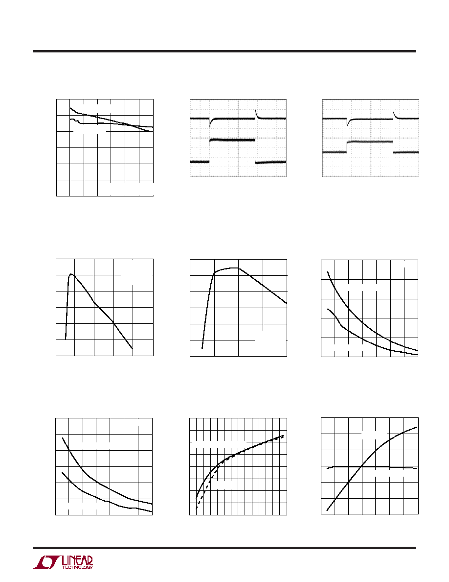
5
LTC3417
3417f
V
IN
(V)
2
2.5
EFFICIENCY (%)
90
95
100
3417 G10
85
80
3
3.5
4
4.5
5
5.5
75
70
V
IN
(V)
2
FREQUENCY VARIATION (%)
0
2
4
5
5.5
3417 G17
≠4
≠10
2.5
3
3.5
4
4.5
6
≠2
≠6
≠8
TEMPERATURE (∞C)
≠50
FREQUENCY VARIATION (%)
5
10
15
25
75
3417 G18
0
≠5
≠25
0
50
100
125
≠10
≠15
V
IN
= 3.6V
V
OUT
= 1.8V
I
LOAD
= 0.25A to 1.4A
REFER TO FIGURE 4
V
IN
= 3.6V
V
OUT
= 2.5V
I
LOAD
= 0.25A to 0.8A
REFER TO FIGURE 4
I
OUT1
500mA/DIV
V
OUT1
100mV/DIV
I
OUT2
500mA/DIV
V
OUT2
100mV/DIV
3417 G11
3417 G12
V
OUT
= 2.5V
REFER TO FIGURE 4
FREQ = 143k TO GROUND
FREQ = 143k TO GROUND
FREQ = V
IN
FREQ = V
IN
I
LOAD
= 800mA
I
LOAD
= 250mA
100
µs/DIV
100
µs/DIV
FREQUENCY (MHz)
0
82
EFFICIENCY (%)
84
86
88
90
92
94
1
2
3
4
3417 G13
5
FREQUENCY (MHz)
0
60
EFFICIENCY (%)
65
70
75
80
85
90
1
2
3
4
3417 G14
V
IN
(V)
2
2.5
0.080
R
DS(ON)
(
)
0.090
0.105
3
4
4.5
3417 G15
0.085
0.100
0.095
3.5
5
5.5
V
IN
(V)
2
R
DS(ON)
(
)
0.18
0.19
0.20
3.5
4.5
3417 G16
0.17
0.16
2.5
3
4
5
5.5
0.15
0.14
T
A =
27
∞C
T
A
= 27
∞C
P-CHANNEL SWITCH
P-CHANNEL SWITCH
N-CHANNEL SWITCH
N-CHANNEL SWITCH
T
A
= 27
∞C
V
IN
= 3.6V
V
OUT
= 2.5V
I
OUT
= 100mA
T
A
= 27
∞C
V
IN
= 3.6V
V
OUT
= 1.8V
I
OUT
= 300mA
OUT2 Efficiency vs V
IN
(Pulse Skipping Mode)
Load Step OUT1
Load Step OUT2
Efficiency vs Frequency OUT1
Efficiency vs Frequency OUT2
R
DS(ON)
vs V
IN
OUT2
Frequency vs V
IN
Frequency vs Temperature
R
DS(ON)
vs V
IN
OUT1
TYPICAL PERFOR A CE CHARACTERISTICS
U
W