1
LTC3444
3444f
WCDMA Applications≠3G Handsets with High Speed
Data Rate Capability
MP3 Players
Digital Cameras
Micropower Synchronous
Buck-Boost DC/DC Converter
for WCDMA Applications
Optimized Features for WCDMA Handsets
Regulated Output with Input Voltages
Above, Below, or Equal to the Output
0.5V to 5V Output Range
Up to 400mA Continuous Output Current From
a Single Lithium-Ion Cell
Minimal External Components
1.5MHz Fixed Frequency Operation
Internal Loop Compensation for Fast Response
<25
µs Full Scale Output Slewing; C
OUT
4.7
µF
Output Disconnect in Shutdown
2.7V to 5.5V Input
<1
µA Shutdown Current
Internal Soft-Start
Output Overvoltage Protection
Single Inductor, No Schottky Diodes Required
Small, Thermally Enhanced 8-Lead (3mm
◊ 3mm)
DFN Package
FEATURES
DESCRIPTIO
U
APPLICATIO S
U
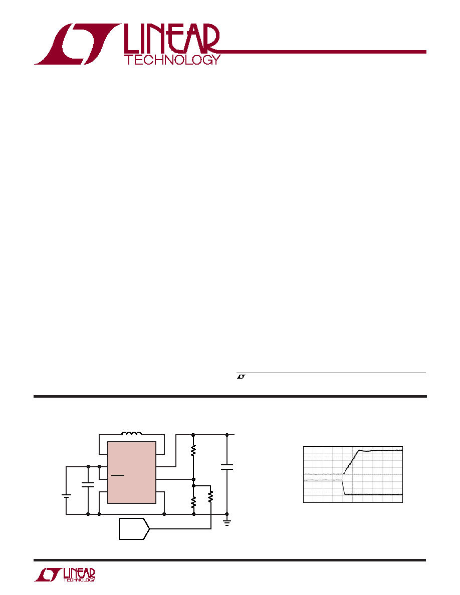
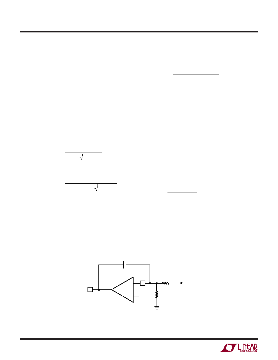
TYPICAL APPLICATIO
U
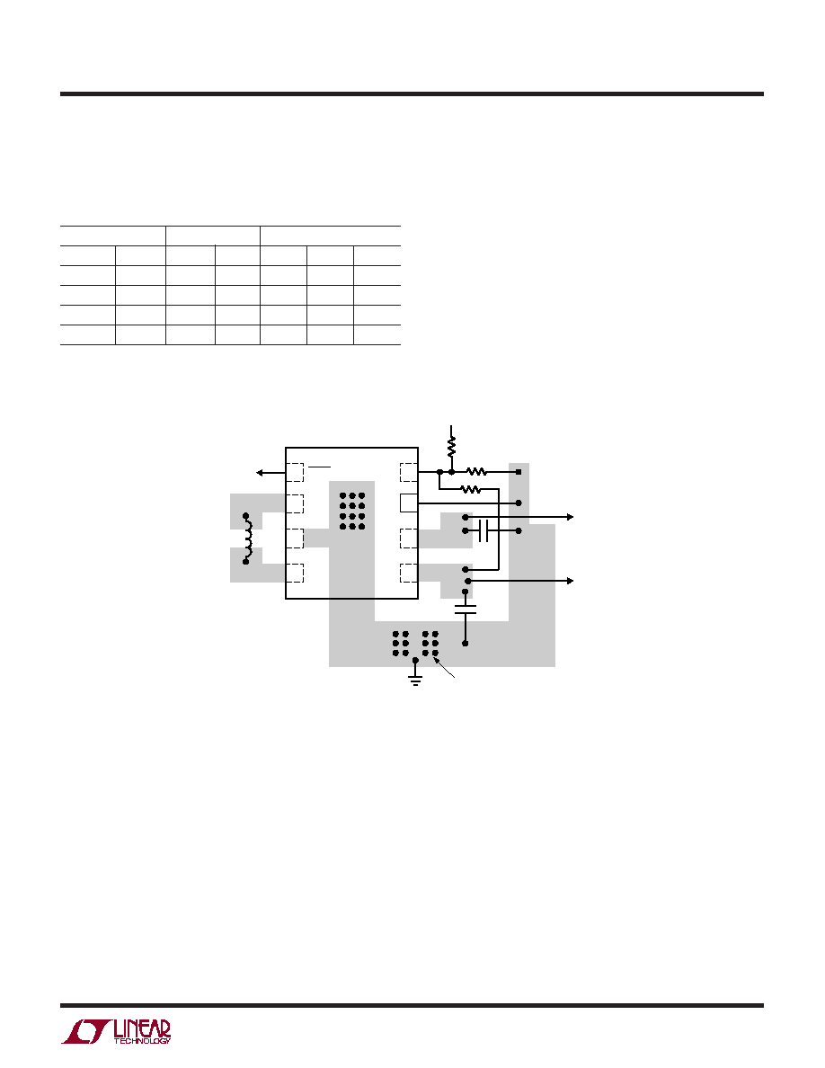
The LTC
Æ
3444 is a highly efficient, fixed frequency, buck-
boost DC/DC converter, which operates from input volt-
ages above, below, and equal to the output voltage. The
topology incorporated in the IC provides a continuous
transfer function through all operating modes, making the
product ideal for a single Lithium-Ion or multi-cell
applications where the output voltage can vary over a wide
range.
The LTC3444 has been optimized for use in 3G WCDMA
applications. A unique design yields high efficiency at
very low output voltages while also eliminating external
components. The high speed error amplifier provides the
fast transient response required to slew the RF power
amplifier from standby to transmit and transmit to stand
by power levels. Output overvoltage protection protects
the RF power amplifier.
Operating frequency is internally set to 1.5MHz to mini-
mize external component size while maximizing efficiency.
Other features include <1
µA shutdown current, internal
soft-start, peak current limit and thermal shutdown. The
LTC3444 is available in a small, thermally enhanced
8-lead (3mm
◊ 3mm) DFN package.
, LTC and LT are registered trademarks of Linear Technology Corporation.
All other trademarks are the property of their respective owners.
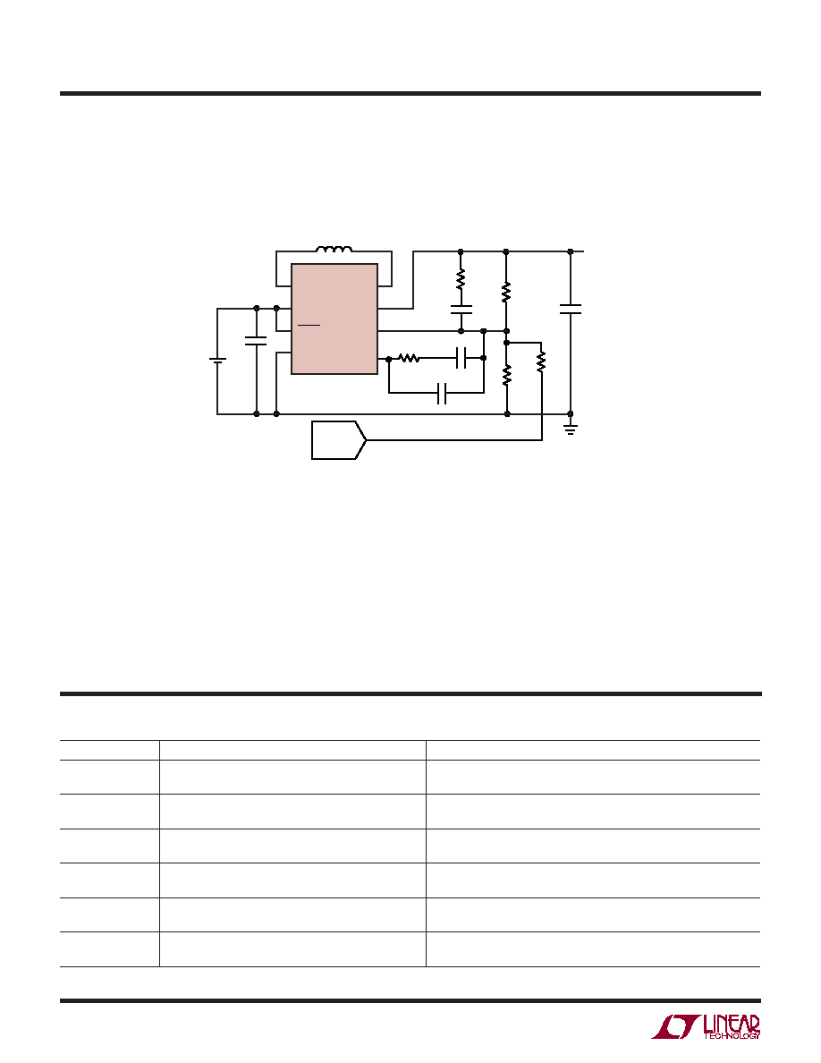
LTC3444
V
CONTROL
3.1V TO 4.2V
SW2
340k
4.7
µF
2.2
µH
4.7
µF
V
OUT
0.8V TO 4.2V
205k
267k
V
OUT
FB
V
C
SW1
V
IN
SHDN
GND
DAC
+
Li-Ion
3444 TA01
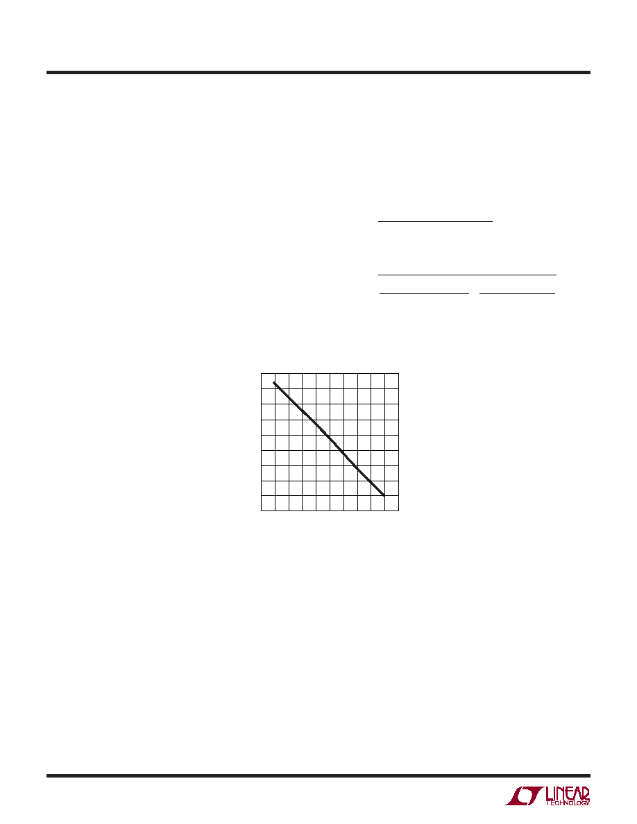
LTC3444 Dynamic Response
V
IN
= 3.6V, V
OUT
= 0.8V TO 4.2V
V
CONTROL
= 2.36V TO 0.28V, I
LOAD
= 100mA
V
CONTROL
10
µs/DIV
1V/DIV
V
OUT
3444 G16a
Protected by U.S. Patents including 6404251, 6166527
.
2
LTC3444
3444f
Consult LTC Marketing for parts specified with wider operating temperature ranges.
ABSOLUTE AXI U RATI GS
W
W
W
U
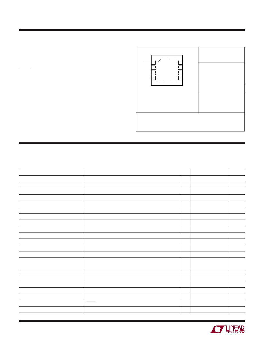
PACKAGE/ORDER I FOR ATIO
U
U
W
(Note 1)
LTC3444EDD
ORDER PART
NUMBER
DD PART MARKING
LBVZ
T
JMAX
= 125
∞C,
JA
= 43
∞C/W,
4-LAYER BOARD
JC
= 2.96
∞C/W
EXPOSED PAD IS GND (PIN 9)
MUST BE SOLDERED TO PCB
The
denotes specifications which apply over the full operating temperature range, otherwise specifications are T
A
= 25
∞C.
V
IN
= V
OUT
=
3.6V unless otherwise noted.
ELECTRICAL CHARACTERISTICS
V
IN
,V
OUT
Voltages .......................................... ≠0.3 to 6V
SW1,SW2 Voltages DC .................................. ≠0.3 to 6V
Pulsed <100ns ............... ≠0.3 to 7V
SHDN Voltage ................................................ ≠0.3 to 6V
Operating Temperature (Note 2) .............. ≠40
∞C to 85∞C
Maximum Junction Temperature (Note 4) ............ 125
∞C
Storage Temperature Range .................. ≠65
∞C to 125∞C
PARAMETER
CONDITIONS
MIN
TYP
MAX
UNITS
Input Start-Up Voltage
2.55
2.65
2.75
V
Output Voltage Adjust Range
0.5
5
V
Feedback Voltage
1.19
1.22
1.25
V
Feedback Input Current
V
FB
= 1.22V
1
50
nA
Quiescent Current - Shutdown
SD = 0V, V
OUT
= 0V Not Including Switch Leakage
0.1
1
µA
Quiescent Current - Active
700
1100
µA
NMOS Switch Leakage
Switches B and C
0.1
7
µA
PMOS Switch Leakage
Switches A and D
0.1
10
µA
NMOS Switch On Resistance
Switches B and C
0.19
PMOS Switch On Resistance
Switches A and D
0.22
PMOS Switch On Resistance
Switch D V
IN
= 3.6, V
OUT
= 1V
0.4
Input Current Limit
2.5
3.5
A
Reverse Current Limit
3
A
Max Duty Cycle
Boost (%Switch C On)
70
82
%
Buck (% Switch A On)
100
%
Min Duty Cycle
0
%
Frequency Accuracy
1.2
1.5
1.8
MHz
Error Amp A
VOL
65
dB
Error Amp Source Current
V
C
= 1.5V, FB = 0V
8
µA
Error Amp Sink Current
V
C
= 1.5V, FB = 1.5V
230
µA
Internal Soft-Start Time
SHDN Going High
250
µs
Output OV Threshold
5.1
5.3
5.5
V
TOP VIEW
DD PACKAGE
8-LEAD (3mm
◊ 3mm) PLASTIC DFN
5
6
7
8
4
3
2
1
9
SHDN
SW1
GND
SW2
FB
V
C
V
IN
V
OUT
Order Options Tape and Reel: Add #TR
Lead Free: Add #PBF Lead Free Tape and Reel: Add #TRPBF
Lead Free Part Marking:
http://www.linear.com/leadfree/
3
LTC3444
3444f
PARAMETER
CONDITIONS
MIN
TYP
MAX
UNITS
SHDN Threshold (On)
IC is Enabled
1.4
V
SHDN Threshold (Off)
IC is Disabled
0.4
V
SHDN Input Current
V
SHDN
= 3.6V
0.01
1
µA
V
C
Output Current
V
C
= GND
0.5
2
µA
ELECTRICAL CHARACTERISTICS
The
denotes specifications which apply over the full operating temperature range, otherwise specifications are T
A
= 25
∞C.
V
IN
= V
OUT
=
3.6V unless otherwise noted.
Note 1: Absolute Maximum Ratings are those values beyond which the life
of a device may be impaired.
Note 2: The LTC3444E is guaranteed to meet performance specifications
from 0
∞C to 85∞C. Specifications over the ≠40∞C to 85∞C operating
temperature range are assured by design, characterization and correlation
with statistical process controls.
Note 3: Current measurements are performed when the outputs are not
switching.
Note 4: This IC includes overtemperature protection that is intended to
protect the device during momentary overload conditions. Junction
temperature will exceed 125
∞C when overtemperature is active.
Continuous operation above the specified maximum operating junction
temperature may result in device degradation or failure.
TYPICAL PERFOR A CE CHARACTERISTICS
U
W
(T
A
= 25
∞C unless otherwise specified)
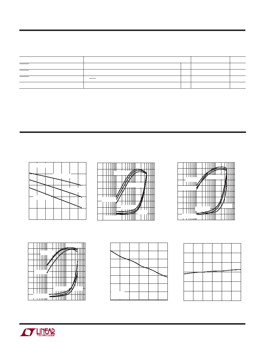
Li-Ion to 1V Efficiency
OUTPUT CURRENT (mA)
20
10
40
30
EFFICIENCY (%)
POWER LOSS (W)
80
70
90
60
50
1
10
100
3444 G06
0
0.04
0.02
0.08
0.06
0.16
0.14
0.18
0.12
0.10
0
1000
V
IN
= 3.6V
V
IN
= 3.1V
V
IN
= 4.4V
V
IN
= 4.4V
V
IN
= 3.1V
PLOSS
Li-Ion to 3.3V Efficiency
OUTPUT CURRENT (mA)
20
10
40
30
EFFICIENCY (%)
POWER LOSS (W)
80
70
90
60
50
1
10
100
3444 G05
0
100
0.15
0.20
0.10
0.05
0
0.25
1000
V
IN
= 3.6V
V
IN
= 3.1V
V
IN
= 4.4V
V
IN
= 3.1V
V
IN
= 3.6V
PLOSS
Efficiency vs V
IN
V
IN
(V)
3.1
3.3
60
EFFICIENCY (%)
70
85
3.5
3.9
4.1
3444 G03
65
80
75
3.7
4.3
4.5
I
OUT
= 100mA
I
OUT
= 65mA
I
OUT
= 50mA
V
OUT
= 1.0V
Operating Frequency
TEMPERATURE (
∞C)
≠55
1.2
FREQUENCY (MHz)
1.3
1.4
1.5
1.6
1.8
≠25
0
35
65
3444 G08
95
125
1.7
Error Amp Source Current
TEMPERATURE (
∞C)
≠55
5
E/A SOURCE CURRENT (
µ
A)
9
13
17
≠25
5
35
65
3444 G07
95
7
11
15
19
125
V
C
= 1V
FB = 0V
Li-Ion to 4.2V Efficiency
OUTPUT CURRENT (mA)
20
10
40
30
EFFICIENCY (%)
POWER
LOSS
(W)
80
70
90
60
50
1
10
100
3444 G04
0
100
0.10
0.05
0.20
0.15
0.40
0.35
0.45
0.30
0.25
0
0.50
1000
V
IN
= 3.6V
V
IN
= 3.1V
V
IN
= 4.4V
V
IN
= 3.1V
V
IN
= 4.4V
PLOSS
4
LTC3444
3444f
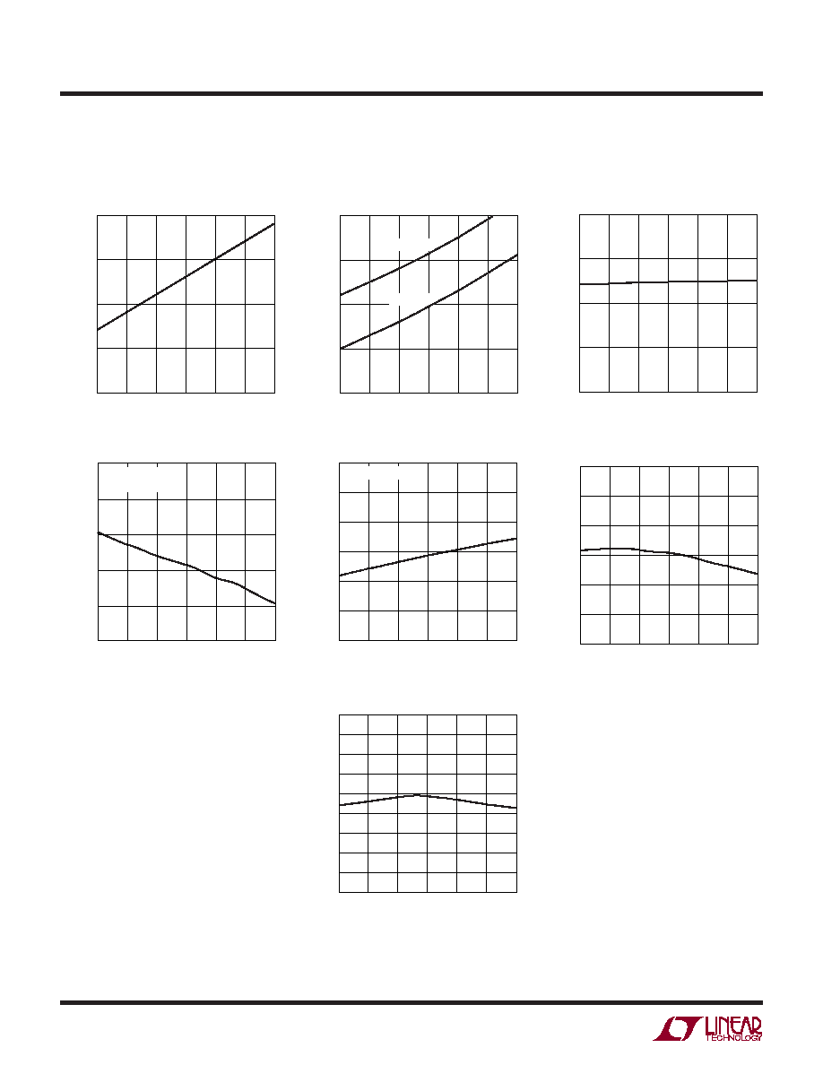
TYPICAL PERFOR A CE CHARACTERISTICS
U
W
PMOS R
DS(ON)
NMOS R
DS(ON)
Boost Maximum Duty Cycle
Error Amp Sink Current
Active Quiescent Current
Feedback Voltage
Minimum Start Voltage
(T
A
= 25
∞C unless otherwise specified)
TEMPERATURE (
∞C)
≠55
0.10
R
DS(ON)
(
)
0.15
0.20
0.25
0.30
≠25
5
35
65
3444 G09
95
125
TEMPERATURE (
∞C)
≠55
0.10
R
DS(ON)
(
)
0.15
0.20
0.25
0.30
≠25
5
35
65
3444 G10
95
125
SWITCH B
SWITCH C
TEMPERATURE (
∞C)
≠55
70
DUTY CYCLE (%)
75
80
85
90
≠25
5
35
65
3444 G11
95
125
TEMPERATURE (
∞C)
≠55
350
E/A SINK CURRENT (
µ
A)
360
370
380
390
400
≠25
5
35
65
3444 G12
95
125
V
IN
= V
OUT
= 3.6V
V
C
= 2V, FB = 3.6V
TEMPERATURE (
∞C)
≠55
V
IN
+ V
OUT
CURRENT (
µ
A)
35
95
3444 G13
≠25
5
65
125
500
550
600
650
700
800
750
V
IN
= V
OUT
= 3.6V
TEMERATURE (
∞C)
≠55
1.19
FEEDBACK VOLTAGE (V)
1.20
1.21
1.22
1.23
1.25
≠25
5
35
65
3444 G14
95
125
1.24
TEMPERATURE (
∞C)
≠55
2.40
START VOLTAGE (V)
2.45
2.55
2.60
2.65
65
2.85
3444 G15
2.50
5
≠25
95
35
125
2.70
2.75
2.80

5
LTC3444
3444f
U
U
U
PI FU CTIO S
SHDN (Pin 1): Shutdown Function. A logic low input shuts
down the IC. A logic high input enables the IC and starts
the internal soft-start function by limiting the rise time of
the internal PWM command.
SW1 (Pin 2): Switch Pin Where the Internal Switches A
and B are Connected. Connect inductor from SW1 to SW2.
An optional Schottky diode can be connected from ground
to SW1 for a moderate efficiency improvement. Minimize
trace length to minimize EMI.
GND (Pin 3): Ground Pin for the IC.
SW2 (Pin 4): Switch Pin Where the Internal Switches C
and D are Connected. An optional Schottky diode can be
connected from SW2 to V
OUT
for a moderate efficiency
improvement. Minimize trace length to keep EMI down.
V
OUT
(Pin 5): Output of the Synchronous Rectifier. A filter
capacitor is placed from V
OUT
to GND. A ceramic bypass
capacitor is recommended as close to the V
OUT
and GND
pins as possible.
V
IN
(Pin 6): Input Supply Pin. Internal V
CC
for the IC. A
4.7
µF ceramic capacitor is recommended as close to V
IN
and GND as possible.
V
C
(Pin 7): Error Amp Output. Pull V
C
to ground to select
internal loop compensation. External compensation may
be connected from V
C
to FB. Internal compensation will be
disabled if V
C
is tied to an external compensation network.
FB (Pin 8): Feedback Pin. Connect resistive divider tap
here. The output voltage can be adjusted from 0.5V to 5V.
The feedback reference voltage is typically 1.22V.
GND (Pin 9, Exposed Pad): Solder to Board GND.
6
LTC3444
3444f
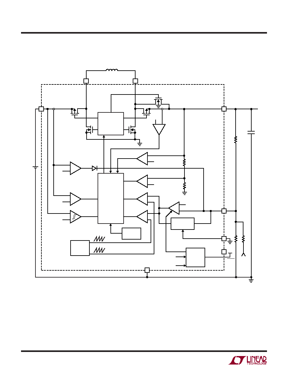
BLOCK DIAGRA
W
3444 BD
+
≠
GATE DRIVERS
AND
ANTI-CROSS
CONDUCTION
3.1V TO 5.5V
V
IN
PWM LOGIC
AND
OUTPUT PHASING
THERMAL
SHUTDOWN
OSC
3A
1.8V
SW2
V
OUT
FB
SHDN
V
OUT
SW1
2.5A
3.5A
2.65V
0.8V
1.22V
THERMAL
SHUTDOWN
GND
SOFTSTART
UVLO
V
IN
OUTLOW
AVERAGE
CURRENT
LIMIT
PEAK
CURRENT
LIMIT
UVLO
PEAK
REVERSE
CURRENT
LIMIT
+
≠
+
≠
+
≠
+
≠
+
≠
OUTPUT OV
+
≠
+
≠
PWM
COMPARATORS
INTERNAL
COMPENSATION
GND = INTERNAL COMP
FLOAT = EXTERNAL COMP
INTERNAL
SOFTSTART
EA
5
6
2
4
8
7
V
CONTROL
1
3
+
V
C
A
B
C
D

7
LTC3444
3444f
OPERATIO
U
The LTC3444 is a highly efficient, fixed frequency, buck-
boost DC/DC converter, which operates from input volt-
ages above, below, and equal to the output voltage. The
topology incorporated in the IC provides a continuous
transfer function through all operating modes, making the
product ideal for single Lithium-Ion or multi-cell applica-
tions where the output voltage can vary over a wide range.
The LTC3444 is designed to provide dynamic voltage
control in space constrained 3G WCDMA applications.
Due to the high operating frequency and integrated loop
compensation a complete WCDMA application requires
only six additional components; input and output capaci-
tors (ceramic), an inductor, and three resistors. The high
speed error amplifier and integrated loop compensation
provide the fast transient response required to slew the RF
power amplifier's voltage rail from standby to transmit
and transmit to standby levels in < 25
µs while minimizing
output overshoot or undershoot.
Efficiency under low output voltage conditions
(standby mode) is improved by using an N-channel
MOSFET in parallel to P-channel MOSFET switch D.
This parallel MOSFET eliminates the need for an external
Schottky. Output overvoltage protection protects the RF
power amplifier from voltages greater than 5.5V.
When used with the proper inductance and output capaci-
tance, the LTC3444 internal compensation is designed to
be consistent with the transient requirements of a typical
WCDMA application. External compensation can be used
with other combinations of inductance and output capaci-
tance, however, the transient response may not be
consistent with typical WCDMA requirements.
Output voltage programming is accomplished via a sum-
ming resistor input to the feedback resistive divider string.
The output voltage varies inversely with the command
voltage. When using the internal loop compensation,
resistor R1 in the feedback resistive divider string must be
340k. There are no constraints on R1 when using external
compensation. However, lower value resistors will de-
crease the resistance value required for programming the
output voltage. Care must be taken not to load down the
control voltage source.
8
LTC3444
3444f
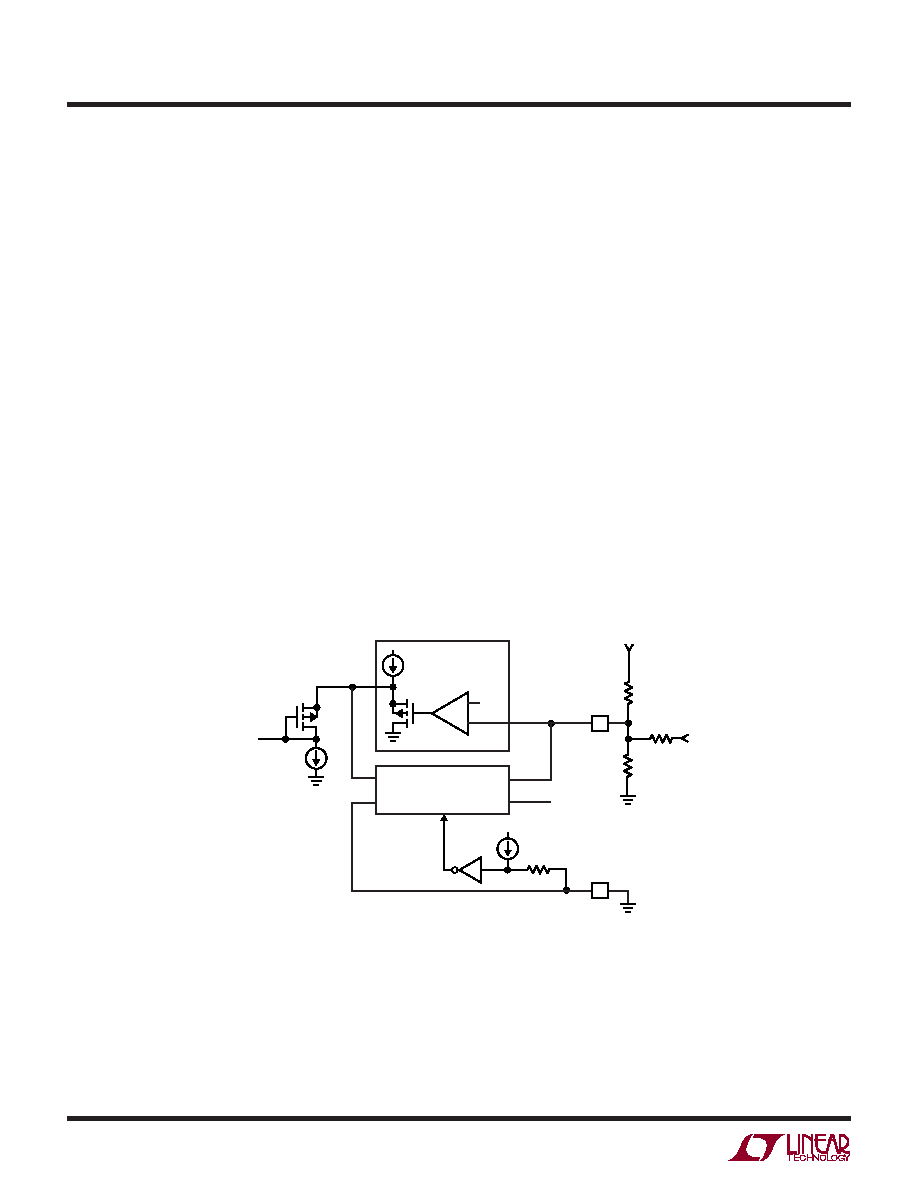
Error Amp
The LTC3444 error amplifier is a voltage mode amplifier.
The internal loop compensation is designed to optimize
transient response to control input change when the
proper output L-C and R1 values are used. Refer to
Figure 1.
Internal loop compensation is selected by grounding the
V
C
pin. The loop is designed to exhibit a single pole roll-off
(≠20dB/dec) with a crossover frequency of ~100KHz.
External compensation can be used by connecting the
compensation components from FB to V
C
. The V
C
pin
must be allowed to float when using external compensa-
tion. If external compensation is used the internal com-
pensation is automatically disabled. A Type III compensa-
tion network is typically required to meet the output
transient requirements of WCDMA.
During start-up, the ramp rate of the error amp output is
controlled to provide a soft-start function. Refer to
Figure 2.
Internal Current Limit
There are two different current limit circuits in the LTC3444.
The two circuits have internally fixed thresholds.
The first circuit sources current out of the FB pin to drop
the output voltage once the peak current exceeds 2.5A
typical. During conditions where V
OUT
is near ground,
such as during a short circuit or during startup, this
threshold is cut in half, providing current foldback
protection.
The second circuit is a high-speed peak current limit
amplifier that shuts off P-channel MOSFET switch A if the
input current exceeds 3.5A typical. The delay to output for
this amplifier is typically 50ns.
OPERATIO
U
0.5
µA
20
µA
V
OUT
V
OUT
V
IN
V
CONTROL
V
C
V
C
FB
3444 F01
INTERNAL
COMPENSATION
NETWORK
GND = INTERNAL
OPEN = EXTERNAL
TO PWM
COMPARATORS
7
+
≠
ERROR AMP
INT
ON
1.22V
R3
R1
R2
8
Figure 1. Error Amplifier with Compensation Select Function
9
LTC3444
3444f
Reverse Current Limit
The LTC3444 always operates in forced continuous con-
duction mode. The reverse current limit amplifier moni-
tors the inductor current from the output through switch
D. Once the negative inductor current exceeds 3A typical,
the LTC3444 will shut off switch D. The high reverse
current is required to meet the transient slew require-
ments for WCDMA power amplifiers.
Output Overvoltage Protection
The LTC3444 provides output overvoltage protection. If
the output voltage exceeds 5.3V typical, P-channel MOSFET
switches A and D are turned off and N-channel MOSFET
switches B and C are turned on. Normal switching will
resume once the output voltage drops below ~5.1V. If the
condition which caused the output overvoltage is still
present the output will charge up to 5.3V again and the
overvoltage cycle will be repeat. Normal output regulation
will resume once the condition responsible for the output
overvoltage is removed.
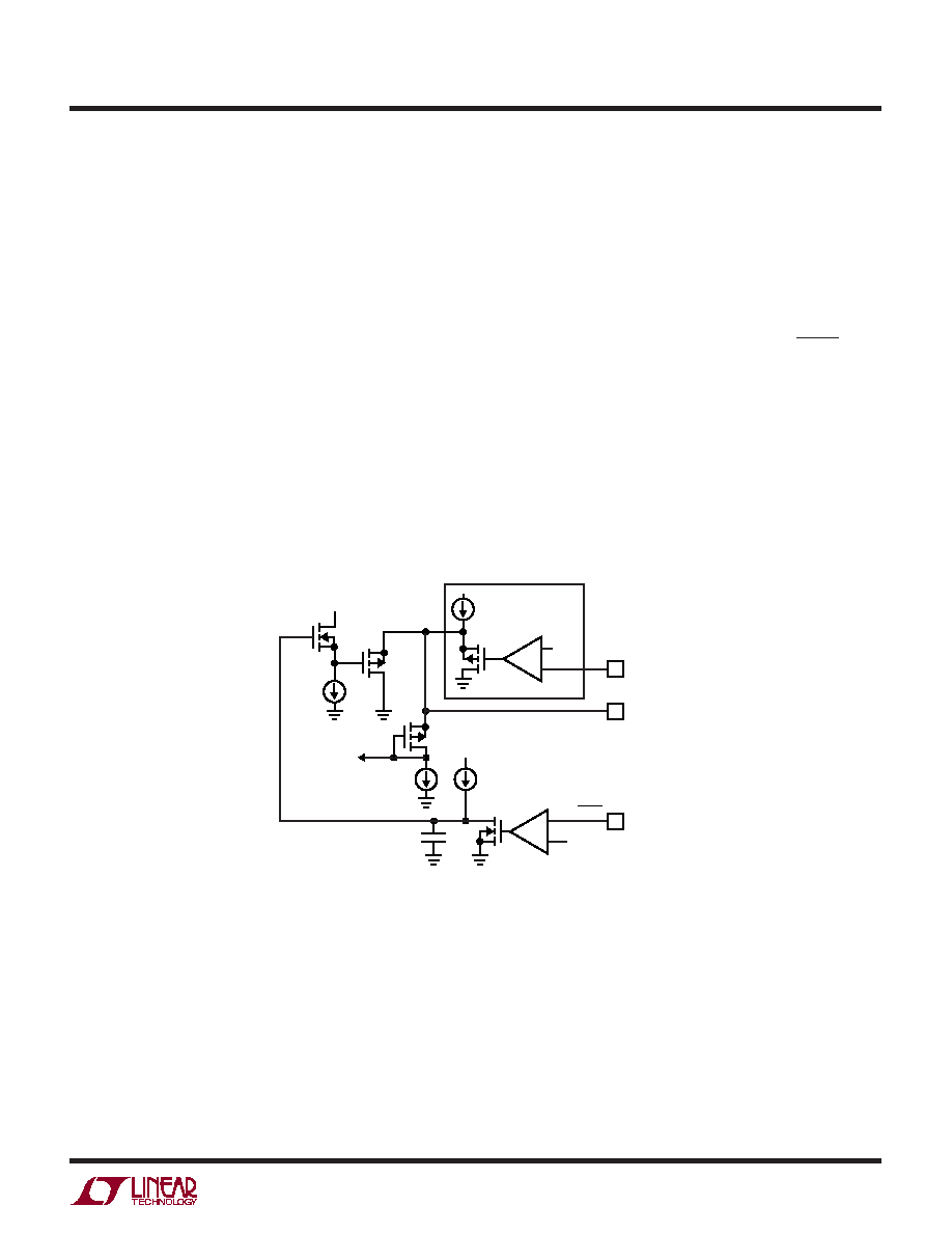
Soft-Start
The soft-start function is initiated when the SHDN pin is
brought above 1.4V and the LTC3444 is out of UVLO
(above minimum input operating specs). The LTC3444 is
enabled but the PWM duty cycle is clamped via the error
amp output. The soft-start time is internally set to 250
µs
to minimize output overshoot. A detailed diagram of this
function is shown in Figure 2.
OPERATIO
U
20
µA
V
CI
I
SS
1V
SHDN
C
SS
V
IN
FB
V
C
3444 F02
TO PWM
COMPARATORS
SOFT-START
CLAMP
+
≠
+
≠
ERROR AMP
1.22V
8
7
1
Figure 2. Soft-Start Circuitry
10
LTC3444
3444f
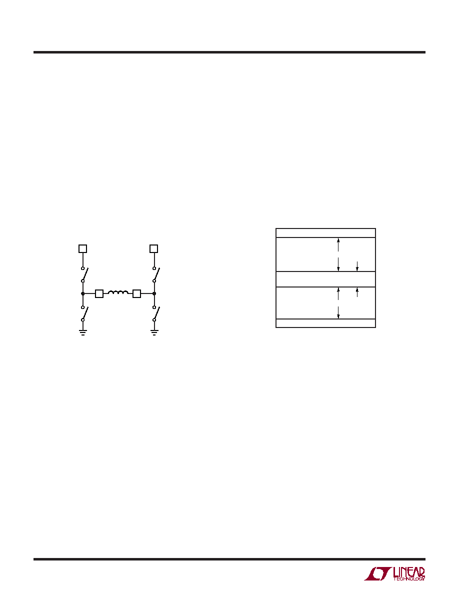
Buck-Boost Four-Switch Control
Figure 3 shows a simplified diagram of how the four
internal switches are connected to the inductor, V
IN
, V
OUT
and GND. Figure 4 shows the regions of operation for the
LTC3444 as a function of the internal control voltage, V
CI
.
Depending on the control voltage, the LTC3444 will oper-
ate in either buck, buck-boost or boost mode. The V
CI
Figure 3. Simplified Diagram of Output Switches
Figure 4. Switch Control vs Internal Control Voltage, V
CI
voltage is a level shifted voltage from the output of the
error amp (V
C
pin) (see Figure 2). The four power switches
are properly phased so the transfer between operating
modes is continuous, smooth and transparent to the user.
The buck-boost region is reached when V
IN
approaches
V
OUT
. The conduction time of the four switch region is
typically 125ns. The three operating modes of the four
switch buck-boost converter are described below. Please
refer to Figures 3 and 4.
OPERATIO
U
6
5
2
4
V
IN
SW1
SW2
PMOS A
PMOS D
NMOS B
NMOS C
V
OUT
3444 F03
A ON, B OFF
PWM CD
SWITCHES
V4 (~1.16V)
V3 (~0.73V)
V2 (~0.49V)
V1 (OV)
DUTY
CYCLE
INTERNAL
CONTROL
VOLTAGE, V
CI
88% D
MAX
BOOST
D
MIN
BOOST
D
MAX
BUCK
0%
D ON, C OFF
PWM AB
SWITCHES
FOUR SWITCH PWM
BUCK-BOOST
REGION
BOOST REGION
BUCK REGION
3444 F04

11
LTC3444
3444f
Buck Region (V
IN
> V
OUT
)
Switch D is always on and switch C is always off during this
mode. When the internal control voltage, V
CI
, is above
voltage V1, Switch A is on. During the off time of switch A,
synchronous switch B turns on for the remainder of the
time. Switches A and B will alternate similar to a typical
synchronous buck regulator. As the control voltage in-
creases, the duty cycle of switch A increases until the
maximum duty cycle of the converter in buck mode
reaches DMAX_BUCK, given by:
DMAX_BUCK = 100% ≠ D4
SW
where D4
SW
= duty cycle % of the four switch range.
D4
SW
= (125ns ∑ f) ∑ 100 %
where f = operating frequency, Hz.
Beyond this point the "four switch," or Buck-Boost region
is reached.
Buck-Boost or Four Switch (V
IN
~ V
OUT
)
When the internal control voltage, V
CI
, is above voltage V2,
but below V3, switch pair AD remain on for duty cycle
DMAX_BUCK, and the switch pair AC begins to phase in.
As switch pair AC phases in, switch pair BD phases out
accordingly. When the V
CI
voltage reaches the edge of the
buck-boost range, at voltage V3, the AC switch pair
completely phase out the BD pair, and the boost phase
begins at duty cycle D4
SW
. The input voltage, V
IN
, where
the four switch region begins is given by:
V
V
ns f
V
IN
OUT
=
∑
1
125
≠ (
)
The point at which the four switch region ends is given by:
V
IN
= V
OUT
(1≠D) = V
OUT
(1≠125ns ∑ f) V
OPERATIO
U
12
LTC3444
3444f
Figure 5. V
OUT
vs V
CONTROL
with R1 = 340k, R2 = 249k, and
R3 = 182k, V
CONTROL
= 0.5V to 2.5V
Boost Region (V
IN
< V
OUT
)
Switch A is always on and switch B is always off during this
mode. When the internal control voltage, V
CI
, is above
voltage V3, switch pair CD will alternately switch to pro-
vide a boosted output voltage. This operation is typical to
a synchronous boost regulator. The maximum duty cycle
of the converter is limited to 82% typical and is reached
when V
CI
is above V4.
CONTROLLING THE OUTPUT VOLTAGE
The output voltage is controlled via a summing resistor
input at the feedback (FB) resistive divider string. Refer to
Figure 1. The output voltage has an inverse relation to the
control voltage as shown in Figure 5. The resistor values
are dependent on the desired output voltage range and the
control voltage range. When using the internal loop com-
pensation, V
C
= GND, R1 must be 340k. For external
compensation R1 should be chosen first and R2 and R3
calculated from the following equations.
The resistor values are given by:
R
V
V
V
V
R
CON MAX
CON MIN
O MAX
O MIN
3
1
=
∑
(
≠
)
≠
(
)
(
)
(
)
(
)
R
V
R
V
R
CON MAX
O MIN
2
1 22
1 22
3
1 22
1
=
.
(
≠ .
)
≠
( .
≠
)
(
)
(
)
OPERATIO
U
V
CONTROL
0
V
OUT
0.5
1.5
2
2.5
2
2.5
4.5
3444 G01
1
0.5
1
1.5
3
3.5
4
13
LTC3444
3444f
Table 1. Shows some typical resistor value combinations
for several V
CONTROL
vs V
OUT
voltage ranges. One percent
(1%) resistor tolerances were assumed.
Table 1. Typical Resistor Values for V
OUT
vs V
CONTROL
V
CONTROL
(V)
V
OUT
(V)
RESISTANCE (k
)
MIN
MAX
MIN
MAX
R1
R2
R3
0.35
2.4
0.8
4.2
340
271
205
0.35
2.5
0.5
5.0
340
210
162
0.8
2.35
0.8
4.2
340
200
154
0.5
2.5
0.5
4.2
340
249
182
Figure 6. Recommended Component Placement
COMPONENT SELECTION
Recommended Component Placement
Figure 6. Shows a recommended component placement.
Traces carrying high current should be made short and
wide. Trace area at FB and V
C
pins should be minimized.
Lead lengths to the battery should be kept short. V
OUT
and
V
IN
ceramic capacitors should be placed close to the IC
pins. Multiple vias should be used between layers.
OPERATIO
U
3444 F06
V
IN
V
IN
V
OUT
LTC3444
MULTIPLE VIAS
5
6
7
8
V
OUT
V
IN
V
C
FB
4
3
2
1
SW2
GND
SW1
SHDN
V
CONTROL
14
LTC3444
3444f
Inductor Selection
The high frequency operation of the LTC3444 allows the
use of small surface mount inductors. The internal loop
compensation is designed to work with a 2.2
µH inductor
(1.5
µH for V
IN
< 3.1V). The 2.2
µH inductor was selected to
optimize the transient response to the control input. The
use of a 2.2
µH inductor pushes out the right half plane
(RHP) zero frequency and allows the loop crossover to
occur at frequencies higher than the output L-C double
pole.
For external compensation the inductor selection is based
on the desired inductor ripple current. The inductor ripple
current is typically set to 20% to 40% of the average
inductor current. Increased inductance results in lower
ripple current, however, higher inductance pulls in the
RHP zero frequency and limits the maximum crossover
frequency possible. Refer to Closing the Feedback Loop
for more information on the RHP zero. For a given ripple
the inductance terms are given as follows:
L
V
V
V
f I
I
V
H
BOOST
IN MIN
OUT
IN MIN
OUT MAX
L
OUT
>
∑
∑
∑
∑
(
)
(
)
(
)
(
≠
)
2
2
L
V
V
V
f I
I
V
H
BUCK
OUT
IN MAX
OUT
OUT MAX
L
IN MAX
>
∑
∑
∑
∑
(
≠
)
(
)
(
)
(
)
where f = operating frequency, Hz
I
L
= inductor ripple current, A
V
IN(MIN)
= minimum input voltage, V
V
IN(MAX)
= maximum input voltage, V
V
OUT
= output voltage, V
I
OUT(MAX)
= maximum output load current
In most cases, the boost configuration will be used to
determine the minimum inductance allowed for a given
ripple current.
For high efficiency, choose a ferrite inductor with a high
frequency core material to reduce core loses. The inductor
should have low ESR (equivalent series resistance) to
reduce the I
2
R losses, and must be able to handle the peak
inductor current without saturating. To minimize radiated
noise, use a shielded inductor. See Table 2 for a suggested
list of inductor suppliers.
Table 2. Inductor Vendor Information
SUPPLIER
PHONE
FAX
WEB SITE
Coilcraft
(847) 639-6400
(847) 639-1469
www.coilcraft.com
CoEv Magnetics
(800) 227-7040
(650) 361-2508
www.circuitprotection.com/magnetics.asp
COOPER Bussmann
(636) 394-2877
1-800-544-2570
www.coooperET.com
Murata
(814) 237-1431
(814) 238-0490
www.murata.com
(800) 831-9172
Sumida
USA: (847) 956-0666
USA: (847) 956-0702
www.sumida.com
Japan: 81(3) 3607-5111
Japan: 81(3) 3607-5144
TDK
(847) 803-6100
(847) 803-6296
www.component.tdk.com
TOKO
(847) 297-0070
(847) 699-7864
www.tokoam.com
OPERATIO
U
15
LTC3444
3444f
Output Capacitor Selection
A 4.7
µF, X5R or X7R type ceramic capacitor should be
used when using the internal loop compensation. When
using external compensation, larger values of output
capacitance can be used, however, larger output capaci-
tance will increase the time needed to slew the output
voltage as required in typical WCDMA applications. The
bulk value of the output filter capacitor is set to reduce the
ripple due to charge into the capacitor each cycle. The
steady state ripple due to charge is given by:
%
_
(
≠
)
%
(
)
RIPPLE BOOST
I
V
V
C
V
f
OUT
OUT
IN MIN
OUT
OUT
=
∑
∑
∑
∑
100
2
%
_
(
≠
)
%
(
)
(
)
(
)
RIPPLE BUCK
I
V
V
C
V
V
f
OUT MAX
IN MAX
OUT
OUT
IN MAX
OUT
=
∑
∑
∑
∑
∑
100
where C
OUT
= output filter capacitor in farads
f = switching frequency in Hz.
In a typical application the output capacitance may be
many times larger than that calculated above in order to
handle the transient load response requirements of the
converter. For a rule of thumb, the ratio of the operating
frequency to the unity-gain bandwidth of the converter is
the amount the output capacitance will have to increase
from the above calculations in order to maintain the
desired transient response. However, in WCDMA applica-
tions the output capacitance should be kept at a minimum
to maximize the output slew rate. Refer to the Loop
Compensation Networks section of this datasheet.
The other component of ripple is due to the ESR (equiva-
lent series resistance) of the output capacitor. Low ESR
capacitors should be used to minimize output voltage
ripple. For surface mount applications, Taiyo Yuden or
TDK ceramic capacitors, AVX TPS series tantalum capaci-
tors or Sanyo POSCAP are recommended. See Table 3 for
contact information.
Ceramic output capacitors should use case size 1206 or
larger. Smaller case sizes have a larger voltage coefficient
that can greatly reduce the output capacitance value at
higher output voltages.
Input Capacitor Selection
Since the V
IN
pin is the supply voltage for the LTC3444, as
well as the input to the power stage of the converter, it is
recommended to place at least a 4.7
µF, X5R or X7R
ceramic bypass capacitor close to the V
IN
and GND pins.
It is also important to minimize any stray resistance from
the converter to the battery or other power source.
OPERATIO
U
Table 3. Capacitor Vendor Information
SUPPLIER
PHONE
FAX
WEB SITE
AVX
(803) 448-9411
(803) 448-1943
www.avxcorp.com
Sanyo
(619) 661-6322
(619) 661-1055
www.sanyovideo.com
Taio Yuden
(408) 573-4150
(408) 573-4159
www.t-yuden.com
TDK
(847) 803-6100
(847) 803-6296
www.component.tdk.com
16
LTC3444
3444f
Optional Schottky Diodes
Schottky diodes across the synchronous switches B and
D are not required, but provide a lower drop during the
break-before-make time (typically 15ns) of the NMOS to
PMOS transition, improving efficiency. Use a surface
mount Schottky diode such as an MBRM120T3 or equiva-
lent. Do not use ordinary rectifier diodes, since the slow
recovery times will compromise efficiency.
Closing the Feedback Loop
The LTC3444 incorporates voltage mode PWM control.
The control to output gain varies with operation region
(buck, boost, buck-boost), but is usually ~20dB. The
output filter exhibits a double pole response, as given by:
f
L C
Hz
in buck
e
FILTER POLE
OUT
_
(
mod )
=
∑ ∑
∑
1
2
f
V
V
L C
Hz
in boost
e
FILTER POLE
IN
OUT
OUT
_
(
mod )
=
∑
∑ ∑
∑
2
where L is in Henries and C
OUT
is in farads.
The output filter zero is given by:
f
R
C
Hz
FILTER ZERO
ESR
OUT
_
=
∑ ∑
∑
1
2
where R
ESR
is the equivalent series resistance of the
output cap.
A troublesome problem when operating in boost mode is
dealing with the right-half plane zero (RHP), given by:
f
V
I
L V
Hz
RHPZ
IN
OUT
OUT
=
∑ ∑
∑ ∑
2
2
The RHP zero has a +20dB/dec gain typical of a zero but
the ≠90
∞ phase lag of a pole. This causes the loop gain to
flatten out while the phase margin decreases. The only way
to combat a RHP zero is to roll off the loop well before the
RHP zero frequency.
LOOP COMPENSATION NETWORKS
A simple Type I compensation network, refer to Figure 7,
can be incorporated to stabilize the loop, but at a cost of
reduced bandwidth and slower transient response. To
ensure proper phase margin using Type I compensation,
the loop must be crossed over at least a decade before the
output LC double pole frequency. The unity-gain fre-
quency of the error amplifier with the Type I compensation
is given by:
f
R
C
Hz
UG
=
∑ ∑ ∑
1
2
1
2
WCDMA applications demand an improved transient re-
sponse to the input control voltage. In other applications,
the output capacitor can be increased to meet help meet
the load transient requirements.
Figure 7. Error Amplifier with Type I Compensation
OPERATIO
U
≠
+
7
8
V
REF
V
OUT
V
C
FB
R2
R1
C2
3444 F07
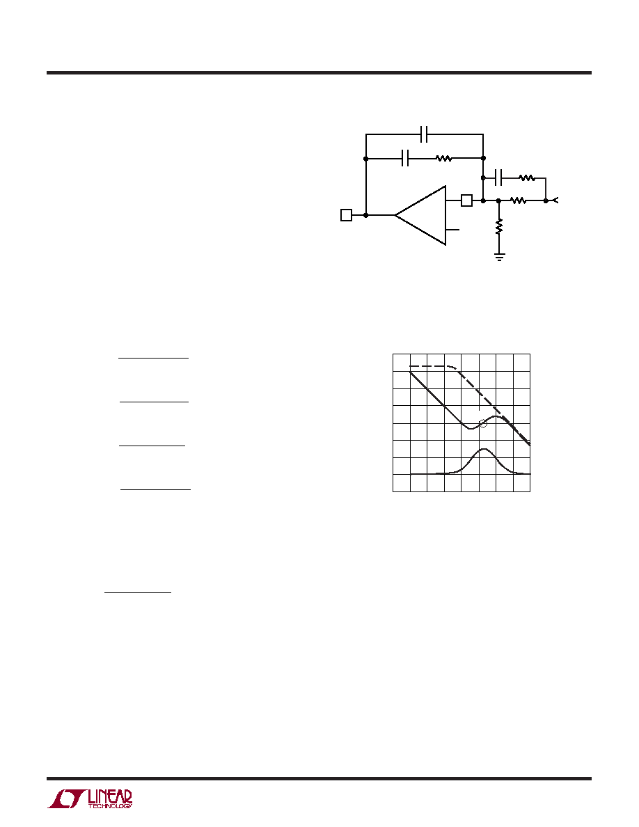
17
LTC3444
3444f
However, due to the output voltage slewing requirements
found in WCDMA applications the output filter capacitor
must be minimized. To maximize the transient response,
while minimizing the output capacitance, a higher band-
width, Type III compensation is required. A Type III
compensation network, refer to Figure 8, has a double zero
to cancel the double pole of the output LC filter and a
double pole to compensate for the ESR zero and RHP zero
of the boost topology. In addition to the double poles,
the Type III network also has a single pole at DC. The
Type III compensation provides a maximum 135
∞ phase
boost and allows the loop crossover to occur at frequen-
cies higher than the output LC. Refer to Figure 9. Referring
to Figure 8, the location of the poles and zeros are given by:
Assume C
2
>> C
3
, R
1
>> R
4
.
f
R
C
Hz
POLE1
1
2
5
3
∑ ∑
∑
f
R
C
Hz
POLE2
1
2
4
1
=
∑ ∑
∑
f
R
C
Hz
ZERO1
1
2
1
1
=
∑ ∑ ∑
f
R
C
Hz
ZERO2
1
2
5
2
=
∑ ∑
∑
And the unity gain frequency (f
UG
) of the Type III compen-
sation is given by:
f
R
C
Hz
UG
=
∑ ∑ ∑
1
2
1
2
where resistance is in ohms and capacitance is in farads.
Note: Bias resistor, R2, does not affect the Pole/Zero
placement.
Figure 9. Frequency Response for LTC3444 Error
Amplifier with a Typical Type III Compensation Network
Figure 8, Error Amplifier with Type III Compensation
OPERATIO
U
≠
+
7
8
V
REF
V
OUT
V
C
FB
R2
R1
R4
C2
R5
C3
3444 F08
C1
FREQUENCY (Hz)
GAIN (db)
PHASE (DEG)
0
40
3444 G02
≠40
≠80
1
e
1
e1
1
e2
1
e3
1
e4
1
e5
1
e6
1
e7
1
e8
80
≠20
20
≠60
60
0
180
≠180
≠360
360
≠90
90
≠270
270
f
UO
18
LTC3444
3444f
Example of Internal Compensation Transient Response for a
Command Voltage Change
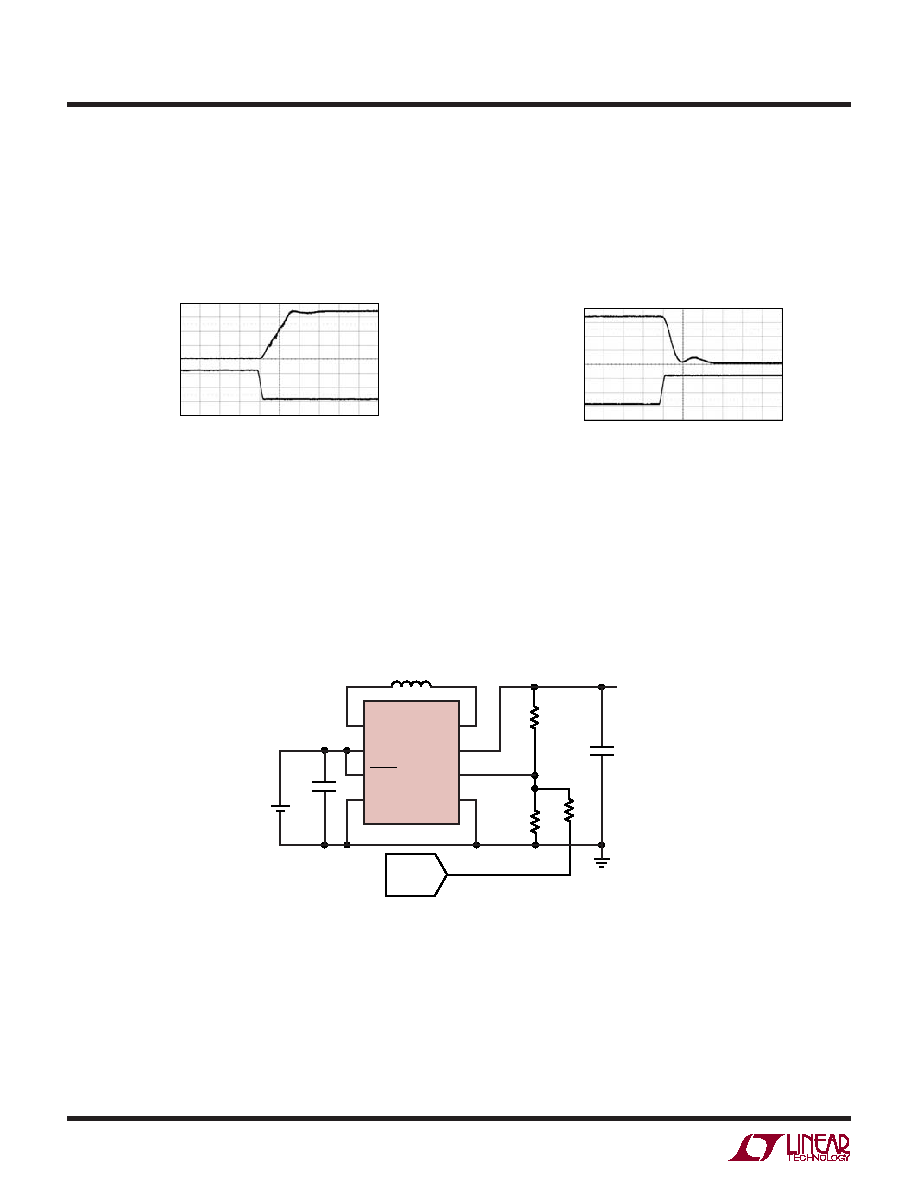
TYPICAL APPLICATIO S
U
LTC3444
V
CONTROL
2.7V TO 4.2V
SW2
R1
340k
C
OUT
4.7
µF
1.5
µH
L1
C
IN
4.7
µF
V
OUT
0.8V TO 4.2V
R3
205k
R2
267k
V
OUT
FB
V
C
SW1
V
IN
SHDN
GND
DAC
+
Li-Ion
3444 TA02
C
IN
=
C
OUT
=
L1 =
MURATA:GRM31CR61C475K
MURATA:GRM31CR61C475K
COOPER BUSSMAN SD12-2R2
Internally Compensated WCDMA Application. Singe Cell, 2.7V to
4.2V Input, 0.8V to 4.2V at 400mA Output.
V
IN
= 3.6V, V
OUT
= 0.8V TO 4.2V
V
CONTROL
= 2.36V TO 0.28V, I
LOAD
= 100mA
V
CONTROL
10
µs/DIV
1V/DIV
V
OUT
3444 G16a
V
IN
= 3.6V, V
OUT
= 4.2V TO 0.8V
V
CONTROL
= 0.28V TO 2.36V, I
LOAD
= 100mA
V
CONTROL
V
OUT
!""" /%
10
µs/DIV
1V/DIV
LTC3444 Dynamic Response
LTC3444 Dynamic Response
19
LTC3444
3444f
Information furnished by Linear Technology Corporation is believed to be accurate and reliable.
However, no responsibility is assumed for its use. Linear Technology Corporation makes no represen-
tation that the interconnection of its circuits as described herein will not infringe on existing patent rights.
U
PACKAGE DESCRIPTIO
3.00
±0.10
(4 SIDES)
NOTE:
1. DRAWING TO BE MADE A JEDEC PACKAGE OUTLINE M0-229 VARIATION OF (WEED-1)
2. DRAWING NOT TO SCALE
3. ALL DIMENSIONS ARE IN MILLIMETERS
4. DIMENSIONS OF EXPOSED PAD ON BOTTOM OF PACKAGE DO NOT INCLUDE
MOLD FLASH. MOLD FLASH, IF PRESENT, SHALL NOT EXCEED 0.15mm ON ANY SIDE
5. EXPOSED PAD SHALL BE SOLDER PLATED
6. SHADED AREA IS ONLY A REFERENCE FOR PIN 1 LOCATION
ON TOP AND BOTTOM OF PACKAGE
0.38
± 0.10
BOTTOM VIEW--EXPOSED PAD
1.65
± 0.10
(2 SIDES)
0.75
±0.05
R = 0.115
TYP
2.38
±0.10
(2 SIDES)
1
4
8
5
PIN 1
TOP MARK
(NOTE 6)
0.200 REF
0.00 ≠ 0.05
(DD8) DFN 1203
0.25
± 0.05
2.38
±0.05
(2 SIDES)
RECOMMENDED SOLDER PAD PITCH AND DIMENSIONS
1.65
±0.05
(2 SIDES)
2.15
±0.05
0.50
BSC
0.675
±0.05
3.5
±0.05
PACKAGE
OUTLINE
0.25
± 0.05
0.50 BSC
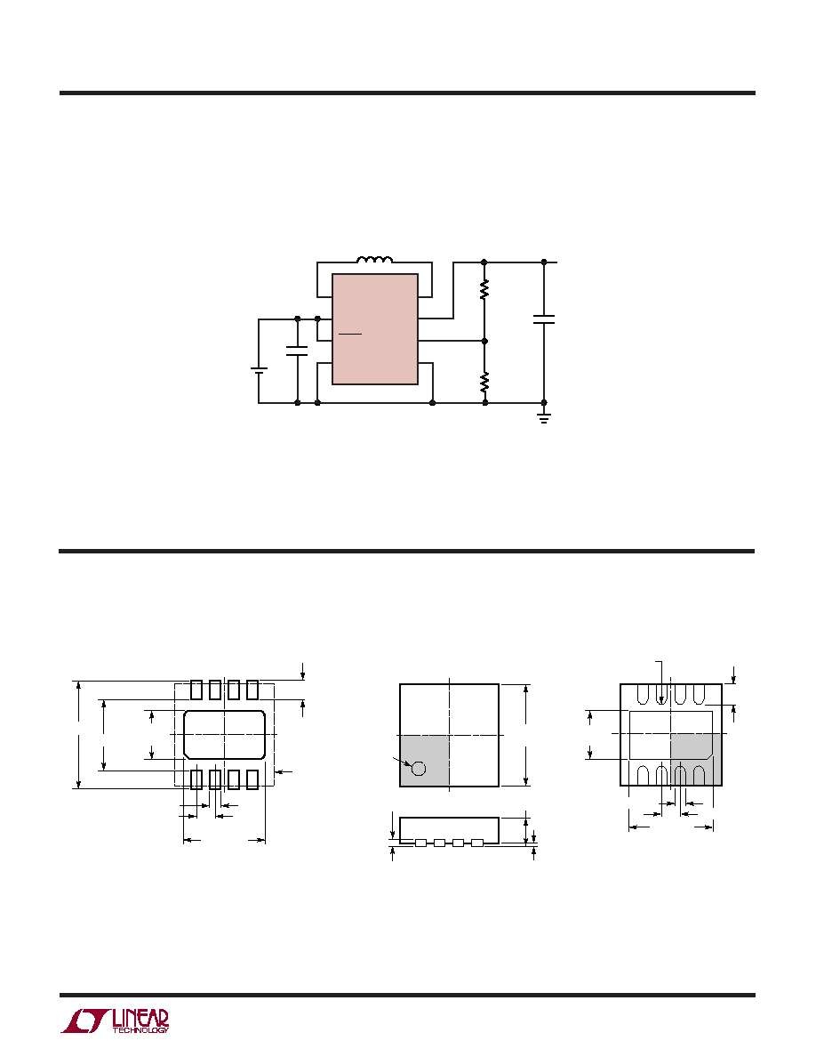
DD Package
8-Lead Plastic DFN (3mm
◊ 3mm)
(Reference LTC DWG # 05-08-1698)
LTC3444
3.1V TO 4.4V
SW2
R1
340k
C
OUT
4.7
µF
2.2
µH
L1
C
IN
4.7
µF
V
OUT
3.3V AT 400mA
R2
200k
V
OUT
FB
V
C
SW1
V
IN
SHDN
GND
+
3444 TA04
Li-Ion
C
IN
=
C
OUT
=
L1 =
MURATA:GRM31CR61C475K
MURATA:GRM31CR61C475K
COOPER BUSSMAN SD12-2R2
Single Li-Ion, 3.1V to 4.2V Input, 3.3V at 400mA
Output with Internal Compensation
TYPICAL APPLICATIO S
U
20
LTC3444
3444f
© LINEAR TECHNOLOGY CORPORATION 2005
LT 1105 ∑ PRINTED IN THE USA
Linear Technology Corporation
1630 McCarthy Blvd., Milpitas, CA 95035-7417
(408) 432-1900
FAX: (408) 434-0507
www.linear.com
PART NUMBER
DESCRIPTION
COMMENTS
LTC3403
1.5MHz, 600mA, Synchronous Step-Down Regulator
96% Efficiency, V
IN
: 2.5V to 5V, V
OUT
: 0.3V to 3.5V,
with Bypass Transistor
I
SD
<1
µA, (3mm ◊ 3mm) DFN Package
LTC3408
1.5MHz, 600mA, Synchronous Step-Down Regulator
96% Efficiency, V
IN
: 2.5V to 5V, V
OUT
: 0.3V to 3.5V,
with Bypass Transistor
I
SD
<1
µA, (3mm ◊ 3mm) DFN Package
LTC3440
Up to 2MHz, 600
µA, Synchronous Buck-Boost
95% Efficiency, V
IN
: 2.5V to 5.5V, V
OUT(MIN)
= 2.5V,
DC/DC Converter
I
SD
<1
µA, I
Q
= 25
µA, 10-Lead MS Package
LTC3441
1MHz, 1.2A, Synchronous Buck-Boost
95% Efficiency, V
IN
: 2.5V to 5.5V V
OUT(MIN)
= 2.5V,
DC/DC Converter
I
SD
<1
µA, I
Q
= 25
µA, 12-Lead (4mm ◊ 3mm) DFN Package
LTC3442
Up to 2MHz, 1.2A, Synchronous Buck-Boost
95% Efficiency, V
IN
: 2.5V to 5.5V, V
OUT(MIN)
= 2.5V,
DC/DC Converter
I
SD
<1
µA, I
Q
= 25
µA, 12-Lead (4mm ◊ 3mm) DFN Package
LTC3443
600MHz, 1.2A Synchronous Buck-Boost
95% Efficiency, V
IN
: 2.5V to 5.5V, V
OUT(MIN)
= 2.5V,
DC/DC Converter
I
SD
<1
µA, I
Q
= 25
µA, 12-Lead (4mm ◊ 3mm) DFN Package
RELATED PARTS
Externally Compensated WCDMA Application. Singe Cell,
3.1V to 4.2V Input, 0.8V to 4.2V at 400mA Output.
LTC3444
V
CONTROL
3.1V TO 4.2V
SW2
R4
47.5k
C
OUT
4.7
µF
3.3
µH
L1
C
IN
4.7
µF
V
OUT
0.8V TO 4.2V
R3
205k
R2
267k
R1
340k
R5
47.5k
C2
220
pF
C3
10
pF
C1
10
pF
V
OUT
FB
V
C
SW1
V
IN
SHDN
GND
DAC
+
Li-Ion
3444 TA03
C
IN
=
C
OUT
=
L1 =
MURATA:GRM31CR61C475K
MURATA:GRM31CR61C475K
COOPER BUSSMAN SD12-3R3
U
TYPICAL APPLICATIO