LTC3450
1
3450f
FEATURES
DESCRIPTIO
U
APPLICATIO S
U
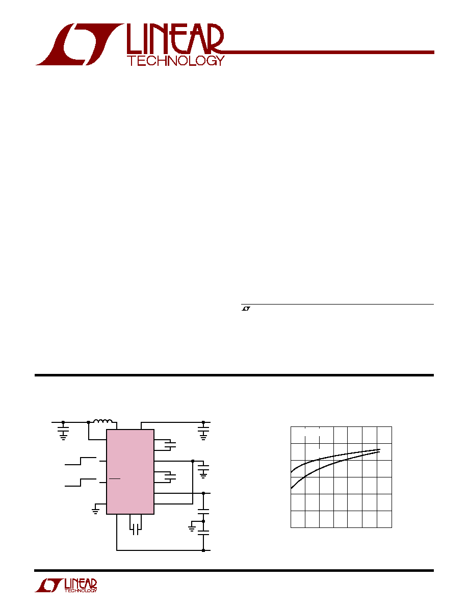
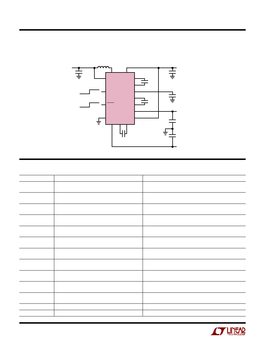
TYPICAL APPLICATIO
U
The LTC
ģ
3450 is a complete power converter solution for
small thin film transistor (TFT) liquid crystal display (LCD)
panels. The device operates from a single Lithium-Ion cell,
2- to 3-cell alkaline input or any voltage source between
1.5V and 4.6V.
The synchronous boost converter generates a low noise,
high efficiency 5.1V, 10mA supply. Internal charge pumps
are used to generate 10V, 15V, and ≠5V, ≠10V or ≠15V.
Output sequencing is controlled internally to insure proper
initialization of the LCD panel.
A master shutdown input reduces quiescent current to
<2
Ķ
A and quickly discharges each output for rapid turn off
of the LCD panel. The LTC3450 is offered in a low profile
(0.8mm max), 3mm
◊
3mm 16-pin QFN package, mini-
mizing the solution profile and footprint.
s
Cellular Handsets with Color Display
s
Handheld Instruments
s
PDA
, LTC and LT are registered trademarks of Linear Technology Corporation.
s
Generates Three Voltages:
5.1V at 10mA
≠ 5V, ≠10, or ≠15V at 500
Ķ
A
10V or 15V at 500
Ķ
A
s
Better than 90% Efficiency
s
Low Output Ripple: Less than 5mV
P-P
s
Complete 1mm Component Profile Solution
s
Controlled Power-Up Sequence: AV
DD
/V
GL
/V
GH
s
All Outputs Disconnected and Actively Discharged in
Shutdown
s
Low Noise Fixed Frequency Operation
s
Frequency Reduction Input for High Efficiency in
Blank Mode
s
Ultralow Quiescent Current: 75
Ķ
A (Typ) in Scan Mode
s
Available in a 3mm
◊
3mm 16-Pin QFN Package
Triple Output Power Supply
for Small TFT-LCD Displays
0.1
Ķ
F
2.2
Ķ
F
V
IN
1.5V TO
4.6V
AV
DD
5.1V/10mA
VGH (3
◊
AV
DD
)
15V/500
Ķ
A
VGL
≠10V/500
Ķ
A
3450 TA01
0.1
Ķ
F
C1
+
C1
≠
0.1
Ķ
F
C2
+
C2
≠
11
7
8
10
14
13
V2X
V3X
V
INV
V
IN
SHDN
MODE
SW
V
OUT
V
NEG
LTC3450
GND
12
15
16
1
2
3
6
5
OFF ON
BLANK SCAN
47
Ķ
H
4
9
2.2
Ķ
F
0.47
Ķ
F
0.1
Ķ
F
0.1
Ķ
F
C3
≠
C3
+
5.1V, ≠10V, 15V Triple Output TFT-LCD Supply
AV
DD
Efficiency vs V
IN
V
IN
(V)
1.5
EFFICIENCY (%)
100
95
90
85
80
75
70
3.0
4.0
3450 TA01b
2.0
2.5
3.5
4.5
5.0
100
Ķ
H
47
Ķ
H
5mA LOAD
LTC3450
2
3450f
V
IN
, SW.......................................................... ≠ 0.3 to 7V
SHDN, MODE ................................................. ≠ 0.3 to 7V
V
OUT ..............................................................................
≠ 0.3 to 7V
V
NEG ........................................................................
≠17V to 0.3V
Operating Temperature Range
LTC3450E (Note 4) ............................. ≠ 40
į
C to 85
į
C
Storage Temperature Range ................. ≠ 65
į
C to 125
į
C
ORDER PART
NUMBER
T
JMAX
= 125
į
C,
JA
= 68
į
C/W
Consult LTC Marketing for parts specified with wider operating temperature ranges.
LTC3450EUD
ABSOLUTE AXI U
RATI GS
W
W
W
U
PACKAGE/ORDER I FOR ATIO
U
U
W
(Note 1) (Referred to GND)
ELECTRICAL CHARACTERISTICS
The
q
denotes the specifications which apply over the full operating
temperature range, otherwise specifications are at T
A
= 25
į
C. V
IN
= 3.6V, V
OUT
= 5.2V unless otherwise noted.
16 15 14 13
5
6
7
8
TOP VIEW
UD PACKAGE
16-LEAD (3mm
◊
3mm) PLASTIC QFN
EXPOSED PAD IS V
NEG
(PIN 17)
MUST BE SOLDERED TO PCB
9
10
11
12
17
4
3
2
1
C3
+
C3
≠
V
NEG
MODE
V2X
C1
+
C1
≠
GND
V
INV
V3X
C2
+
C2
≠
SHDN
V
IN
V
OUT
SW
UD PART MARKING
LAAC
PARAMETER
CONDITIONS
MIN
TYP
MAX
UNITS
Input Voltage Range
q
1.5
4.6
V
V
IN
Quiescent Supply Current
MODE = V
IN
75
130
Ķ
A
V
OUT
Quiescent Supply Current
MODE = V
IN
80
Ķ
A
V
IN
Quiescent Supply Current
MODE = GND
30
50
Ķ
A
V
OUT
Quiescent Supply Current
MODE = GND
13
Ķ
A
V
IN
Quiescent Current
SHDN = GND
0.01
2
Ķ
A
5V Boost Regulator
V
OUT
Output Voltage
Load on V5X = 5mA
5.049
5.100
5.151
V
V
OUT
Efficiency
Load on V5V = 5mA, (Note 2)
90
%
V
OUT
Maximum Output Current
L = 47
Ķ
H, (Note 2)
11
mA
Switch Current Limit
90
120
mA
Switching Frequency--Boost
MODE = V
IN
550
kHz
Switching Frequency--Boost
MODE = GND
15.62
kHz
Charge Pumps
V2X Output Voltage
Load on V2X = 100
Ķ
A
q
9.792
10.1
10.608
V
LTC3450
3
3450f
ELECTRICAL CHARACTERISTICS
The
q
denotes the specifications which apply over the full operating
temperature range, otherwise specifications are at T
A
= 25
į
C. V
IN
= 3.6V, V
OUT
= 5.2V unless otherwise noted.
PARAMETER
CONDITIONS
MIN
TYP
MAX
UNITS
Note 1: Absolute Maximum Ratings are those values beyond which the life
of a device may be impaired.
Note 2: Specification is guaranteed by design and not 100% tested in
production.
V3X Output Voltage
Load on V3X = 100
Ķ
A
q
14.688
15.2
15.912
V
V2X Efficiency
Load on V2X = 100
Ķ
A, (Note 2)
90
%
V3X Efficiency
Load on V3X = 100
Ķ
A, (Note 2)
80
%
Output Impedance V2X, V3X
Flying Capacitors = 0.1
Ķ
F
1
k
V
NEG
Output Voltage
Load on V
NEG
= 100
Ķ
A, V
INV
= V2X
q
≠10.608
≠10.1
≠ 9.792
V
V
NEG
Efficiency
Load on V
NEG
= 100
Ķ
A (Note 2)
80
%
Output Impedance V
NEG
Flying Capacitor = 0.1
Ķ
F
1
k
Switching Frequency Charge Pumps
MODE = V
IN
62.5
kHz
Switching Frequency Charge Pumps
MODE = GND
3.75
kHz
V
NEG
to V3X Delay
(Note 3)
3
4
10
ms
Logic Inputs
SHDN Pin Threshold
q
0.4
0.77
1.2
V
MODE Pin Threshold
1.6
V
Note 3: Measured from point at which V
NEG
crosses ≠5V to point at which
C2
≠
starts switching.
Note 4: The LTC3450E is guaranteed to meet performance specifications
from 0
į
C to 70
į
C. Specifications over the ≠ 40
į
C to 85
į
C operating
temperature range are assured by design, characterization and correlation
with statistical process controls.

LTC3450
4
3450f
TYPICAL PERFOR A CE CHARACTERISTICS
U
W
EFFICIENCY (%)
100
95
90
85
80
75
70
EFFICIENCY (%)
100
95
90
85
80
75
70
V
IN
(V)
1.5
3.0
4.0
2.0
2.5
3.5
4.5
5.0
V
IN
(V)
1.5
3.0
4.0
2.0
2.5
3.5
4.5
5.0
V
IN
(V)
1.5
3.0
4.0
2.0
2.5
3.5
4.5
5.0
V
IN
(V)
1.5
3.0
4.0
2.0
2.5
3.5
4.5
5.5
5.0
V
IN
(V)
1.5
3.0
4.0
2.0
2.5
3.5
4.5
5.5
5.0
3450 G02
3450 G03
AV
DD
(V)
5.16
5.14
5.12
5.10
5.08
5.06
5.04
3450 G06
V
GH
(V)
15.6
15.4
15.2
15.0
14.8
14.6
14.4
V
IN
CURRENT (
Ķ
A)
100
90
80
70
60
50
40
30
20
10
0
3450 G04
V
IN
CURRENT (
Ķ
A)
3450 G05
800
700
600
500
400
300
200
100
V
GH
LOAD (
Ķ
A)
0 100
300
500
700
900
200
400
600
800
3450 G07
1000
V
GL
LOAD (
Ķ
A)
0 100
300
500
700
900
200
400
600
800
1000
V
GL
(V)
≠ 9.0
≠ 9.2
≠ 9.4
≠ 9.6
≠ 9.8
≠ 10.0
≠ 10.2
≠ 10.4
3450 G08
TEMPERATURE (
į
C)
≠ 40 ≠ 25
3450 G09
≠10 5 20 35 50 65 80 95 110 125
AV
DD
(V)
5.200
5.175
5.150
5.125
5.100
5.075
5.050
5.025
5.000
10mA
2mA
0mA
2mA
10mA
2mA
5mA
5mA
5mA
10mA
L = 47
Ķ
H
L = 100
Ķ
H
AV
DD
Efficiency vs V
IN
AV
DD
Efficiency vs V
IN
No Load V
IN
Current in Blank Mode
No Load V
IN
Current in Scan Mode
AV
DD
vs V
IN
and Load
V
GH
vs Load
V
GL
vs Load
AV
DD
vs Temperature
Figure 1 Circuit, 1mA Load
(T
A
= 25
į
C unless otherwise noted)

LTC3450
5
3450f
TYPICAL PERFOR A CE CHARACTERISTICS
U
W
AV
DD
5mV/DIV
(AC)
1
Ķ
s/DIV
V
IN
= 3.6V
C2 = 2.2
Ķ
F
3450 G10
AV
DD
100mV/DIV
(AC)
AV
DD
LOAD
5mA/DIV
100
Ķ
s/DIV
5mA
1mA
V
IN
= 3.6V
C2 = 2.2
Ķ
F
3450 G11
V
GH
10V/DIV
AV
DD
5V/DIV
V
GL
5V/DIV
2ms/DIV
0
0
V
IN
= 3.6V
C2 = 2.2
Ķ
F
3450 G12
0
0
INDUCTOR
CURRENT
100mA/DIV
AV
DD
2V/DIV
20
Ķ
s/DIV
V
IN
= 3.6V
3450 G13
AV
DD
Ripple Voltage
AV
DD
Load = 5mA
AV
DD
Transient Response
AV
DD
, V
GL
, V
GH
Turn-On and
Turn-Off Sequence
AV
DD
Turn-On Showing Inrush
Current Limiting
LTC3450
6
3450f
PI FU CTIO S
U
U
U
C3
+
(Pin 1): Charge Pump Inverter Flying Capacitor Posi-
tive Node. The charge pump inverter flying capacitor is
connected between C3
+
and C3
≠
. The voltage on C3
+
will
alternate between GND and V
INV
at an approximate 50%
duty cycle while the inverting charge pump is operating.
Use a 10nF or larger X5R type ceramic capacitor for best
results.
C3
≠
(Pin 2): Charge Pump Inverter Flying Capacitor Nega-
tive Node. The charge pump inverter flying capacitor is
connected between C3
+
and C3
≠
. The voltage on C3
≠
will
alternate between GND and V
NEG
at an approximate 50%
duty cycle while the inverting charge pump is operating.
Use a 10nF or larger X5R type ceramic capacitor for best
results.
V
NEG
(Pin 3): Charge Pump Inverter Output. V
NEG
can be
either ≠ 5V or ≠10V depending on where V
INV
is con-
nected. V
NEG
should be bypassed to GND with at 0.1
Ķ
F or
larger X5R type ceramic capacitor. V
NEG
can also be
configured for ≠15V with two external low current Schottky
diodes (see Applications section).
MODE (Pin 4): Drive MODE high to force the LTC3450 into
high power (scan) mode. Drive MODE low to force the
LTC3450 into low power (blank) mode. The output volt-
ages remain active with the MODE pin driven low but with
reduced output current capability. MODE must be pulled
up to V
IN
or higher on initial application of power in order
for proper initialization to occur.
SHDN (Pin 5): Master Shutdown Input for the LTC3450.
Driving SHDN low disables all IC functions and reduces
quiescent current from the battery to less than 2
Ķ
A. Each
generated output voltage is actively discharged to GND in
shutdown through internal pull down devices. An optional
RC network on SHDN provides a slower ramp up of the
boost converter inductor current during startup (soft-start).
V
IN
(Pin 6): Input Supply to the LTC3450. Connect V
IN
to
a voltage source between 1.5V and 4.6V. Bypass V
IN
to
GND with a 2.2
Ķ
F X5R ceramic capacitor.
V
OUT
(Pin 7): Main 5.1V Output of the Boost Regulator and
Input to the Voltage Doubler Stage. Bypass V
OUT
with a low
ESR, ESL ceramic capacitor (X5R type) between 2.2
Ķ
F and
10
Ķ
F.
SW (Pin 8): Switch Pin. Connect the inductor between SW
and V
IN
. Keep PCB trace lengths as short and wide as
possible to reduce EMI and voltage overshoot. If the
inductor current falls to zero, the internal P-channel
MOSFET synchronous rectifier is turned off to prevent
reverse charging of the inductor and an internal switch
connects SW to V
IN
to reduce EMI.
GND (Pin 9): Signal and Power Ground for the LTC3450.
Provide a short direct PCB path between GND and the
(≠) side of the output filter capacitor(s) on V
OUT
, V2X, V3X
and V
NEG
.
C1
≠
(Pin 10): Charge Pump Doubler Flying Capacitor
Negative Node. The charge pump doubler flying capacitor
is connected between C1
+
and C1
≠
. The voltage on C1
≠
will
alternate between GND and V
OUT
at an approximate 50%
duty cycle while the charge pump is operating. Use a 10nF
or larger X5R type ceramic capacitor for best results.
C1
+
(Pin 11): Charge Pump Doubler Flying Capacitor
Positive Node. The charge pump doubler flying capacitor
is connected between C1
+
and C1
≠
. The voltage on C1
+
will
alternate between V
OUT
and V2X at an approximate 50%
duty cycle while the charge pump is operating. Use a 10nF
or larger X5R type ceramic capacitor for best results.
V2X (Pin 12): Charge Pump Doubler Output. This output
is 10.2V (nom) at no load and is capable of delivering up
to 500
Ķ
A to a load. V2X should be bypassed to GND with
a 0.47
Ķ
F X5R type ceramic capacitor.
C2
≠
(Pin 13): Charge Pump Tripler Flying Capacitor Nega-
tive Node. The charge pump tripler flying capacitor is
connected between C2
+
and C2
≠
. The voltage on C2
≠
will
alternate between GND and V
OUT
at an approximate 50%
duty cycle while the charge pump is operating. Use a 10nF
or larger X5R type ceramic capacitor for best results.
C2
+
(Pin 14): Charge Pump Tripler Flying Capacitor Posi-
tive Node. The charge pump tripler flying capacitor is
connected between C2
+
and C2
≠
. The voltage on C2
+
will
alternate between V2X and V3X at an approximate 50%
duty cycle while the charge pump is operating. Use a 10nF
or larger X5R type ceramic capacitor for best results.
LTC3450
7
3450f
PI FU CTIO S
U
U
U
CF1
0.1
Ķ
F
C1
2.2
Ķ
F
V
IN
1.5V TO
4.6V
AV
DD
5.1V/10mA
VGH (3
◊
AV
DD
)
15V/500
Ķ
A
10V
VGL
≠10V/500
Ķ
A
3450 TA01
C1
+
C1
≠
V2X
V
IN
SHDN
GLOBAL SHUTDOWN
MODE
SW
V
OUT
OFF ON
BLANK SCAN
L1
47
Ķ
H
C2
2.2
Ķ
F
C7
1
Ķ
F
8
6
4
5
7
9
11
10
12
SHUTDOWN
SYNCHRONOUS
PWM BOOST
CONVERTER
OSCILLATOR
CHARGE PUMP
DOUBLER
IN
OUT
CF2
0.1
Ķ
F
C2
+
C2
≠
V3X
C8
0.47
Ķ
F
14
13
15
SHUTDOWN
SHUTDOWN
CHARGE PUMP
TRIPLER
IN
69kHz
550kHz
OUT
CF3
0.1
Ķ
F
C3
+
C3
≠
V
NEG
GND
C11
0.47
Ķ
F
1
V
INV
16
2
3
SHUTDOWN
CHARGE PUMP
INVERTER
IN
OUT
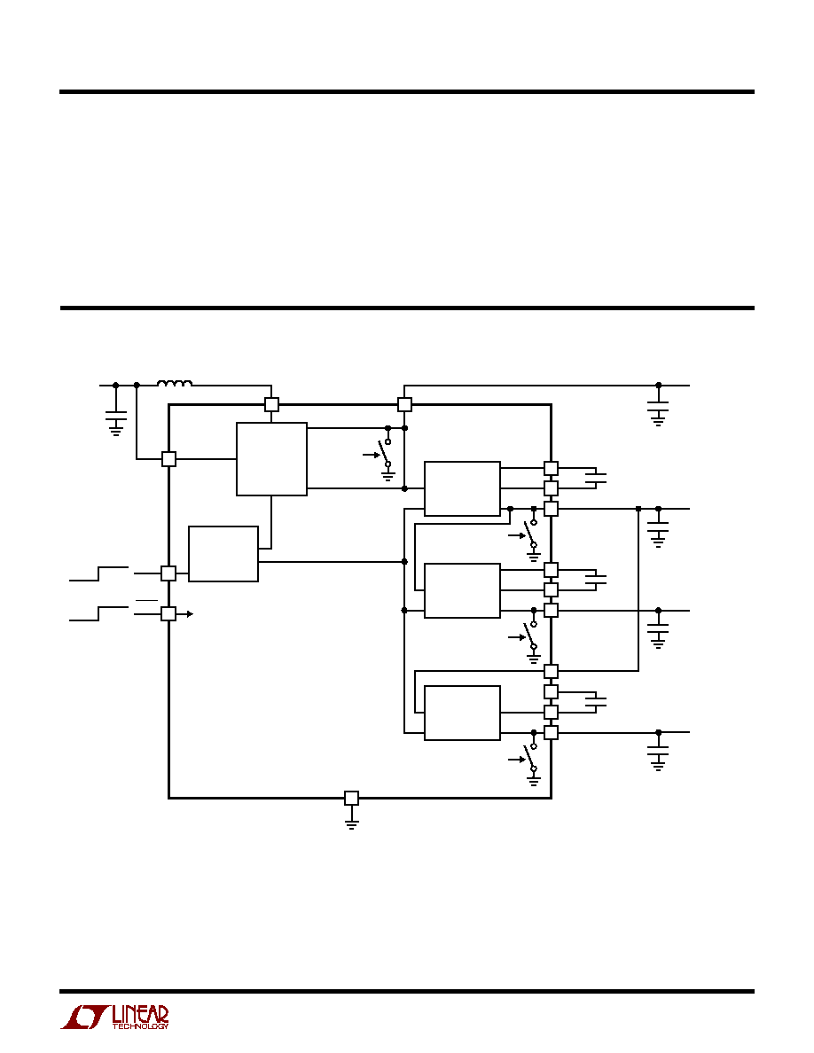
BLOCK DIAGRA
W
V3X (Pin 15): Charge Pump Tripler Output. This output is
15.3V (nom) at no load and is capable of delivering up to
500
Ķ
A to a load. V3X should be bypassed to GND with a
0.1
Ķ
F X5R type ceramic capacitor.
V
INV
(Pin 16): Positive Voltage Input for the Charge Pump
Inverter. The charge pump inverter will generate a nega-
tive voltage corresponding to the voltage applied to V
INV
.
Connecting V
INV
to 5V or 10V will generate ≠5V or ≠10V
respectively on V
NEG
. See Applications section for ≠15V
generation.
Exposed Pad
(Pin 17): The exposed pad must be con-
nected to V
NEG
(Pin 3) on the PCB.
Do not connect the
exposed pad to GND.
LTC3450
8
3450f
OPERATIO
U
The LTC3450 is a highly integrated power converter in-
tended for small TFT-LCD display modules. A fixed fre-
quency, synchronous PWM boost regulator generates a
low noise 5.1V, 10mA bias at greater than 90% efficiency
from an input voltage of 1.5V to 4.6V. Three charge pump
converters use the 5.1V output to generate 10V, 15V and
≠5V, ≠10V or ≠15V at load currents up to 500
Ķ
A. Each
converter is frequency synchronized to the main 500kHz
(nominal) boost converter. The generated output voltages
are internally sequenced to insure proper initialization of
the LCD panel. A digital shutdown input rapidly discharges
each generated output voltage to provide a near instanta-
neous turn-off of the LCD display.
Boost Converter
The synchronous boost converter utilizes current mode
control and includes internally set control loop and slope
compensation for optimized performance and simple de-
sign. Only three external components are required to
complete the design of the 5.1V, 10mA boost converter.
The high operation frequency produces very low output
ripple and allows the use of small low profile inductors and
tiny external ceramic capacitors. The boost converter also
disconnects its output from V
IN
during shutdown to avoid
loading the input power source. Softstart produces a
controlled ramp of the converter input current during
startup, reducing the burden on the input power source.
Very low operating quiescent current and synchronous
operation allow for greater than 90% conversion effi-
ciency.
The MODE input reduces the boost converter operating
frequency by approximately 8x when driven high and
reduces the output power capability of the boost con-
verter. MODE is asserted when the polysilicon TFT-LCD
display is in its extremely low power blank condition. The
boost converter further reduces its quiescent current in
this mode, delivering both lower input (battery) current
drain and low noise operation.
Charge Pumps
The LTC3450 includes three separate charge pump con-
verters which generate 10V, 15V and either ≠5V, ≠10V or
≠15V. Each output can deliver a maximum of 500
Ķ
A. The
charge pumps feature fixed frequency, open-loop opera-
tion for high efficiency and lowest noise performance. The
charge pump converters operate at 1/8 the boost con-
verter frequency and include internal charge transfer
switches. Thus, each charge pump requires only two small
external capacitors, one to transfer charge, and one for
filtering. Similar to the boost converter, the charge pumps
operating frequency reduces to approximately 4kHz in
blank mode, maintaining low noise operation but at re-
duced output current capability.
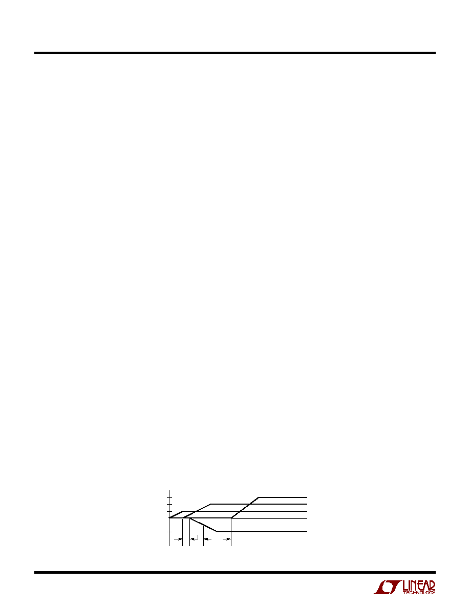
Output Sequencing
Refer to the following text and Figure 1 for the LTC3450
power-up sequence. When input power is applied, the
boost converter initializes and charges its output towards
the final value of 5.1V. When the boost converter output
reaches approximately 90% of its final value (4.5V), an
internal 5V OK signal is asserted which allows the charge
pump doubler to begin operation toward its final goal of
10V. Approximately 1ms later, the charge pump inverter
begins operation toward its final goal of either
≠5V or ≠10V depending on the connection of the V
INV
input. When the ≠5V or ≠10V output (V
NEG
) reaches
approximately 50% of its final value, a 4ms (nominal)
timeout period begins. At the conclusion of the 4ms
timeout period, the charge pump tripler is allowed to
begin operation, which will eventually charge V3X to 15V
(nominal).
≠10V
5V
V
OUT
V
NEG
VX2
VX3
10V
15V
1ms
3450 F01
4ms
Figure 1. Output Sequencing
LTC3450
9
3450f
Inductor Selection
Inductors in the range of 47
Ķ
H to 100
Ķ
H with saturation
current (I
SAT
) ratings of at least 150mA are recommended
for use with the LTC3450. Ferrite core materials are
strongly recommended for their superior high frequency
performance characteristics. A bobbin or toroid type core
will reduce radiated noise. Inductors meeting these re-
quirements are listed in Table 1.
Table 1. Recommended Inductors
PART
L
MAX DCR HEIGHT
NUMBER
(
Ķ
H)
(
)
(mm)
VENDOR
CLQ4D10-470
47
1.28
1.2
Sumida
CLQ4D10-101
100
3.15
(847) 956-0666
CMD4D08-470
47
1.6
1.0
www.sumida.com
DO1606-473
47
1.1
2.0
Coilcraft
DO1606-104
100
2.3
(847) 639-6400
DT1608-473
47
0.34
2.92
www.coilcraft.com
DT1608-104
100
1.1
LQH43MN470J03 47
1.5
2.6
Murata
LQH43MN101J03 100
2.5
www.murata.com
DU6629-470M
47
0.64
2.92
Coev Magnetics
DU6629-101M
100
1.27
www.circuitprotection.com
Capacitor Selection
The boost converter requires two capacitors. The input
capacitor should be an X5R type of at least 1
Ķ
F. The V
OUT
capacitor should also be an X5R type between 2.2
Ķ
F and
10
Ķ
F. A larger capacitor (10
Ķ
F) should be used if lower
output ripple is desired or the output load required is close
to the 10mA maximum.
The charge pumps require flying capacitors of at least
0.1
Ķ
F to obtain specified performance. Ceramic X5R types
are strongly recommended for their low ESR and ESL and
capacitance versus bias voltage stability. The filter capaci-
tor on V2X should be at least 0.1
Ķ
F. A 0.47
Ķ
F or larger
capacitor on V2X is recommended if V
INV
is connected to
V2X. The filter capacitors on V3X and V
NEG
should be
0.1
Ķ
F or larger. Please be certain that the capacitors used
are rated for the maximum voltage with adequate safety
margin. Refer to Table 2 for a listing of capacitor vendors.
Table 2. Capacitor Vendor Information
Supplier
Phone
Website
AVX
(803) 448-9411
www.avxcorp.com
Murata
(714) 852-2001
www.murata.com
Taiyo Yuden
(408) 573-4150
www.t-yuden.com
APPLICATIO S I FOR ATIO
W
U
U
U
Soft-Start
Soft-start operation provides a gradual increase in the
current drawn from the input power source (usually a
battery) during initial startup of the LTC3450, eliminating
the inrush current which is typical in most boost convert-
ers. This reduces stress on the input power source, boost
inductor and output capacitor, reduces voltage sag on the
battery and increases battery life. The rate at which the
input current will increase is set by two external compo-
nents (R
SS
and C
SS
) connected to SHDN (refer to Figure
2). Upon initial application of power or release of a pull
down switch on SHDN, the voltage on SHDN will increase
relative to the R ∑ C time constant or R
SS
∑ C
SS
. After one
time constant SHDN will rise to approximately 63.2% of
the voltage on V
IN
. From 0V to approximately 0.65V on
SHDN, no switching will occur because the shutdown
threshold is 0.65V (typ). From 0.65V to 1V the maximum
switch pin current capability of the LTC3450 will gradually
increase from near zero to the maximum current limit. An
R
SS
in the range of 1M
to 10M
is recommended. If
SHDN is driven high with a logic signal, the input current
will gradually increase to its maximum value in approxi-
mately 50
Ķ
s.
5 SHDN
3450 F02
C
SS
6.8nF
R
SS
1M
5%
1ms SOFT-START WITH 3.6V V
IN
V
IN
Figure 2. Soft-Start Component Configuration
Printed Circuit Board Layout Guidelines
High speed operation of the LTC3450 demands careful
attention to PCB layout. You will not get advertised perfor-
mance with careless layout. Figure 3 shows the recom-
mended component placement for a single layer PCB. A
multilayer board with a separate ground plane is ideal but
not absolutely necessary.
LTC3450
10
3450f
APPLICATIO S I FOR ATIO
W
U
U
U
Figure 3. Suggested Layout
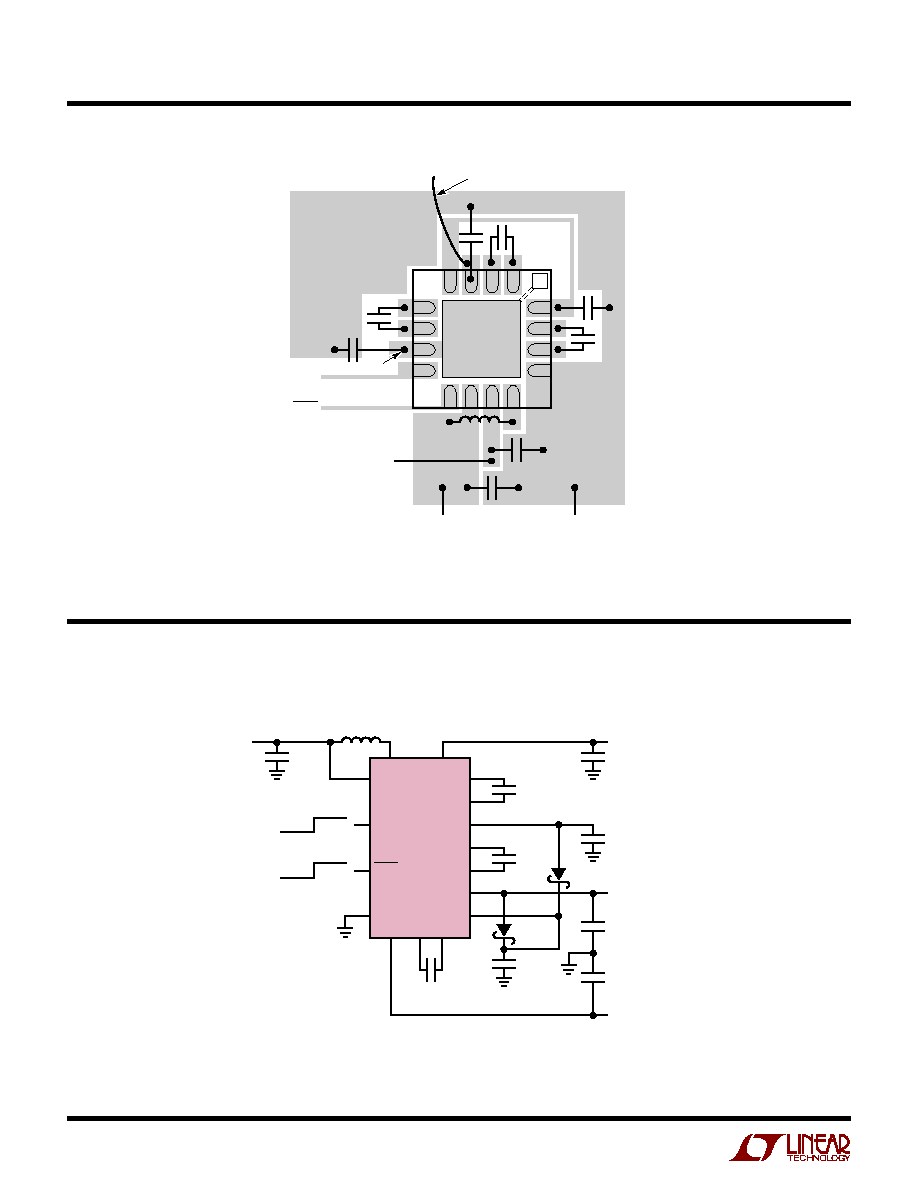
TYPICAL APPLICATIO
U
CF1
0.1
Ķ
F
C1
2.2
Ķ
F
V
IN
1.5V TO
4.6V
D1, D2: DUAL SCHOTTKY DIODE, PANASONIC MA704WKCT
L1: SUMIDA CMD4D08-470
AV
DD
5.1V/10mA
VGH
15V/500
Ķ
A
D1
D2
VGL
≠15V/500
Ķ
A
3450 TA02
CF3
0.1
Ķ
F
CF2
0.1
Ķ
F
11
10
14
13
V2X
V3X
V
INV
V
IN
MODE
SW
V
OUT
V
NEG
C3
≠
C3
+
LTC3450
GND
12
15
16
1
2
3
6
5
OFF ON
BLANK SCAN
L1
47
Ķ
H
4
9
C2
2.2
Ķ
F
0.1
Ķ
F
C4
0.47
Ķ
F
C6
0.1
Ķ
F
C5
0.1
Ķ
F
7
8
C1
+
C1
≠
C2
+
C2
≠
SHDN
5.1V, ≠15V, 15V Triple Output TFT-LCD Supply
V
NEG
NOTE: QFN PACKAGE EXPOSED PAD
IS CONNECTED TO THE V
NEG
PIN.
DO NOT CONNECT EXPOSED PAD TO GROUND
MODE
SHDN
3450 F03
V
OUT
GND
V
IN
V3X
JUMPER
LTC3450
11
3450f
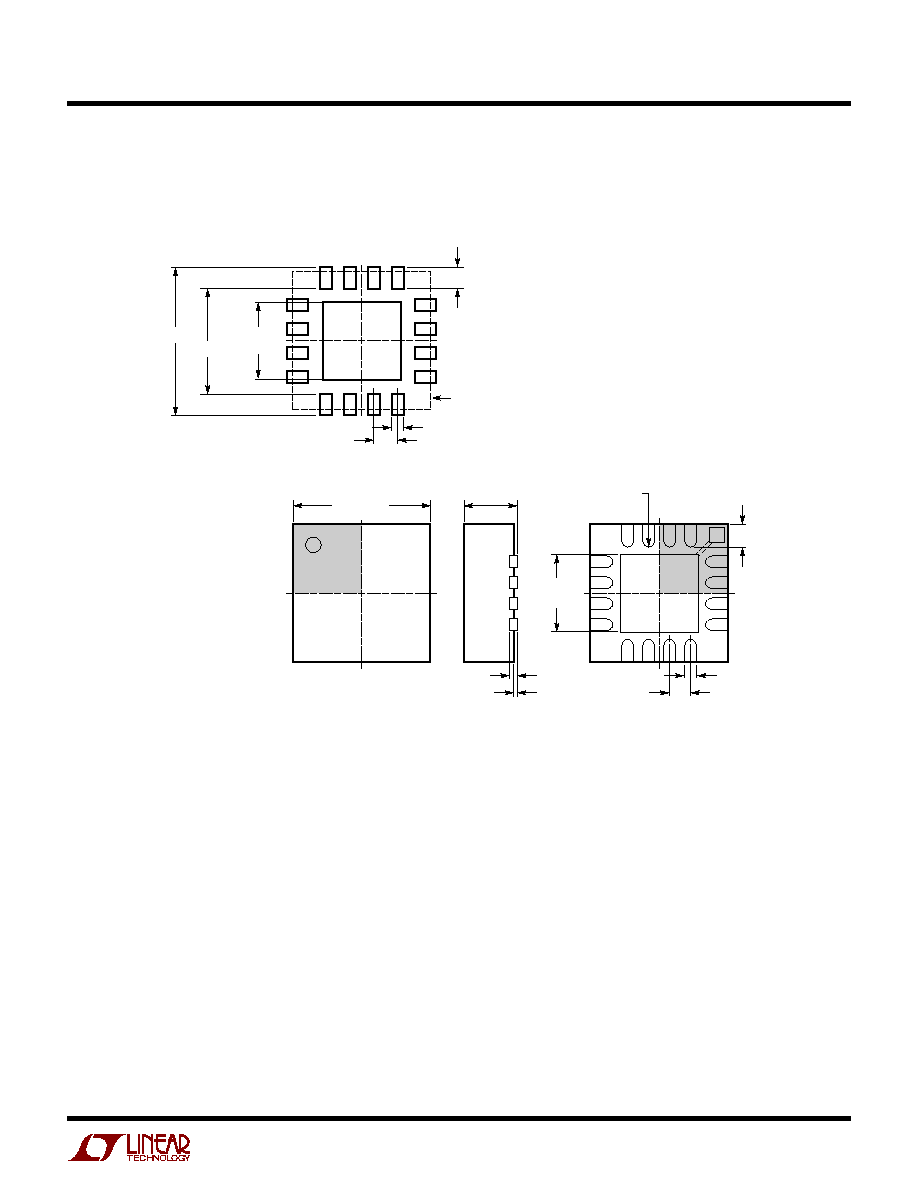
PACKAGE DESCRIPTIO
U
UD Package
16-Lead Plastic QFN (3mm
◊
3mm)
(Reference LTC DWG # 05-08-1691)
3.00
Ī
0.10
(4 SIDES)
RECOMMENDED SOLDER PAD PITCH AND DIMENSIONS
1.45
Ī
0.05
(4 SIDES)
NOTE:
1. DRAWING CONFORMS TO JEDEC PACKAGE OUTLINE MO-220 VARIATION (WEED-2)
2. ALL DIMENSIONS ARE IN MILLIMETERS
3. DIMENSIONS OF EXPOSED PAD ON BOTTOM OF PACKAGE DO NOT INCLUDE
MOLD FLASH. MOLD FLASH, IF PRESENT, SHALL NOT EXCEED 0.15mm ON ANY SIDE
4. EXPOSED PAD SHALL BE SOLDER PLATED
PIN 1
TOP MARK
0.40
Ī
0.10
BOTTOM VIEW--EXPOSED PAD
1.45
Ī
0.10
(4-SIDES)
0.75
Ī
0.05
R = 0.115
TYP
0.23
Ī
0.05
1
15
16
2
0.50 BSC
0.200 REF
2.20
Ī
0.05
3.35
Ī
0.05
0.57
Ī
0.05
0.00 ≠ 0.05
(UD) QFN 0802
0.23
Ī
0.05
0.50 BCS
PACKAGE OUTLINE
Information furnished by Linear Technology Corporation is believed to be accurate and reliable.
However, no responsibility is assumed for its use. Linear Technology Corporation makes no represen-
tation that the interconnection of its circuits as described herein will not infringe on existing patent rights.
LTC3450
12
3450f
Linear Technology Corporation
1630 McCarthy Blvd., Milpitas, CA 95035-7417
(408) 432-1900
q
FAX: (408) 434-0507
q
www.linear.com
©
LINEAR TECHNOLOGY CORPORATION 2003
RELATED PARTS
TYPICAL APPLICATIO
U
PART NUMBER
DESCRIPTION
COMMENTS
LT1310
1.5A I
SW
, 4.5MHz,
V
IN
: 2.75V to 18V, V
OUT
= 35V, I
Q
= 12mA, I
SD
= <1
Ķ
A
High Efficiency Step-Up DC/DC Converter
MSE Package
LT1613
550mA I
SW
, 1.4MHz,
V
IN
: 0.9V to 10V, V
OUT
= 34V, I
Q
= 3mA, I
SD
= <1
Ķ
A
High Efficiency Step-Up DC/DC Converter
ThinSOT Package
LT1615/LT1615-1
300mA/80mA I
SW
, Constant Off-Time,
V
IN
: 1.2V to 15V, V
OUT
= 34V, I
Q
= 20
Ķ
A, I
SD
= <1
Ķ
A
High Efficiency Step-Up DC/DC Converter
ThinSOT Package
LT1940
Dual Output 1.4A I
OUT
, Constant 1.1MHz,
V
IN
: 3V to 25V, V
OUT
(MIN) = 1.2V, I
Q
= 2.5mA, I
SD
= <1
Ķ
A
High Efficiency Step-Down DC/DC Converter
TSSOP-16E Package
LT1944
Dual Output 350mA I
SW
, Constant Off-Time,
V
IN
: 1.2V to 15V, V
OUT
= 34V, I
Q
= 20
Ķ
A, I
SD
= <1
Ķ
A
High Efficiency Step-Up DC/DC Converter
MS Package
LT1944-1
Dual Output 150mA I
SW
, Constant Off-Time,
V
IN
: 1.2V to 15V, V
OUT
= 34V, I
Q
= 20
Ķ
A, I
SD
= <1
Ķ
A
High Efficiency Step-Up DC/DC Converter
MS Package
LT1945
Dual Output, Pos/Neg, 350mA I
SW
, Constant Off-Time,
V
IN
: 1.2V to 15V, V
OUT
=
Ī
34V, I
Q
= 20
Ķ
A, I
SD
= <1
Ķ
A
High Efficiency Step-Up DC/DC Converter
MS Package
LT1946/LT1946A
1.5A I
SW
, 1.2MHz/2.7MHz,
V
IN
: 2.45V to 16V, V
OUT
= 34V, I
Q
= 3.2mA, I
SD
= <1
Ķ
A
High Efficiency Step-Up DC/DC Converter
MS8 Package
LT1947
Triple Output ( for TFT-LCD) 1.1A I
SW
,
V
IN
: 2.7V to 8V, V
OUT
= 34V, I
Q
= 9.5mA, I
SD
= <1
Ķ
A
3MHz High Efficiency Step-Up DC/DC Converter
MS Package
LT1949/LT1949-1
550mA I
SW
, 600kHz/1.1MHz,
V
IN
: 1.5V to 12V, V
OUT
= 28V, I
Q
= 4.5mA, I
SD
= <25
Ķ
A
High Efficiency Step-Up DC/DC Converter
S8, MS8 Packages
LTC3400/LTC3400B
600mA I
SW
, 1.2MHz,
V
IN
: 0.85V to 5V, V
OUT
= 5V, I
Q
= 19
Ķ
A/300
Ķ
A, I
SD
= <1
Ķ
A
Synchronous Step-Up DC/DC Converter
ThinSOT Package
LTC3401
1A I
SW
, 3MHz, Synchronous Step-Up DC/DC Converter
V
IN
: 0.5V to 5V, V
OUT
= 5V, I
Q
= 38
Ķ
A, I
SD
= <1
Ķ
A, MS Package
LTC3402
2A I
SW
, 3MHz, Synchronous Step-Up DC/DC Converter
V
IN
: 0.5V to 5V, V
OUT
= 5V, I
Q
= 38
Ķ
A, I
SD
= <1
Ķ
A, MS Package
5.1V, ≠ 5V, 15V Triple Output TFT-LCD Supply
CF1
0.1
Ķ
F
C1
2.2
Ķ
F
V
IN
1.5V TO
4.6V
L1: SUMIDA CMD4D08-470
AV
DD
5.1V/10mA
VGH (3
◊
AV
DD
)
15V/500
Ķ
A
VGL
≠5V/500
Ķ
A
3450 TA03
CF3
0.1
Ķ
F
CF2
0.1
Ķ
F
11
7
8
10
14
13
V2X
V3X
V
INV
V
IN
MODE
SW
V
OUT
V
NEG
LTC3450
GND
12
15
16
1
2
3
6
5
OFF ON
BLANK SCAN
L1
47
Ķ
H
4
9
C2
2.2
Ķ
F
C4
0.47
Ķ
F
C6
0.1
Ķ
F
C5
0.1
Ķ
F
C1
+
C1
≠
C2
+
C2
≠
SHDN
C3
≠
C3
+
LT/TP 1203 1K ∑ PRINTED IN USA