LTC3531/
LTC3531-3.3/LTC3531-3
1
3531f
FEATURES
DESCRIPTIO
U
APPLICATIO S
U
TYPICAL APPLICATIO
U
INPUT VOLTAGE (V)
1.5
EFFICIENCY (%)
80
90
5.5
3531 TA01b
70
60
2.5
3.5
4.5
2
3
4
5
100
75
85
65
95
BOOST
MODE
4SW
MODE
3.3V
OUT
AT 100mA
BUCK
MODE
The LTC
Æ
3531/LTC3531-3.3/LTC3531-3 are synchronous
buck-boost DC/DC converters that operate from input
voltages above, below or equal to the output voltage. The
topology incorporated in the ICs provides a continuous
transfer through all operating modes, making the product
ideal for single cell Li-Ion and multicell alkaline or nickel
applications. The converters operate in Burst Mode, mini-
mizing solution footprint and component count as well as
providing high conversion effi ciency over a wide range of
load currents.
The devices include two 0.5 N-channel MOSFET switches
and two P-channel switches (0.5, 0.8). Quiescent
current is typically 16µA, making the parts ideal for bat-
tery power applications. Other features include a <1µA
shutdown current, current limiting, thermal shutdown
and output disconnect. The parts are offered in a 6-pin
ThinSOT
TM
package for fi xed voltage versions or a 3mm ◊
3mm DFN package for fi xed and adjustable versions.
200mA Buck-Boost
Synchronous DC/DC
Converters
Regulated Output with Input Above, Below or Equal
to the Output
Single Inductor
Up to 90% Effi ciency
V
IN
Range: 1.8V to 5.5V
200mA at 3.3V
OUT
from 3.6V Input
125mA at 3V
OUT
from 2.5V Input
Fixed V
OUT
Versions (TSOT, DFN): 3.3V, 3V
Adjustable V
OUT
Version (DFN): 2V to 5V
Burst Mode
Æ
Operation, No External Compensation
Ultra Low Quiescent Current: 16µA, Shutdown
Current <1µA
Only 3 External Components Required
Short-Circuit Protection
Output Disconnect in Shutdown
Available in 6-Pin ThinSOT and 3mm ◊ 3mm DFN
Packages
Effi ciency vs V
IN
Handheld Instruments
MP3 Players
Handheld computers
PDA/GPS
, LTC and LT are registered trademarks of Linear Technology Corporation.
All other trademarks are the property of their respective owners.
Burst Mode is a registered trademark of Linear Techonology Corporation.
ThinSOT is a trademark of Linear Techonology Corporation.
Protected by U.S. Patents including 6166527.
SW1
SW2
SHDN
GND
V
IN
V
OUT
LTC3531-3.3
2.2
µF
10
µF
ON OFF
Li-Ion
10
µH
V
IN
3.1V TO
4.2V
V
OUT
3.3V
160mA
3531 TA01a
+
LTC3531/
LTC3531-3.3/LTC3531-3
2
3531f
ABSOLUTE
AXI U
RATI GS
W
W
W
U
FOR ATIO
PACKAGE/ORDER I
U
U
W
ELECTRICAL CHARACTERISTICS
The
denotes the specifi cations which apply over the full operating
temperature range, otherwise specifi cations are at T
A
= 25∞C. V
IN
= 3.6V V
OUT
= 3.3V unless otherwise noted.
V
IN
, V
OUT
, SWA, SWB, SHDN Voltage .............≠0.3 to 6V
SWA, SWB Voltage, <100ns Pulse ..................≠0.3 to 7V
Operating Temperature Range (Note 2) ... ≠40∞C to 85∞C
(Note 1)
Storage Temperature Range ................... ≠65∞C to 125∞C
Lead Temperature (TS6, Soldering, 10 sec) .......... 300∞C
PARAMETER
CONDITIONS
MIN
TYP
MAX
UNITS
V
IN
Minimum Startup Voltage
1.65 1.8
V
V
OUT
Regulation
Output Voltage (3.3V Version)
No Load
3.25 3.32 3.39
V
Output Voltage (3V Version)
No Load
2.95
3.02 3.09
V
FB Voltage (Adj Version)
No Load
1.20 1.225 1.25
V
FB Input Current (Adj Version)
V
FB
= 1.225V
1
50
nA
Operating Current
Quiescent Current in Sleep:
V
IN
V
IN
= 5V, V
OUT
= 3.6V, FB = 1.3V
16
30
µA
V
OUT
V
OUT
= 3.6V
6
10
µA
Shutdown Current
V
IN
SHDN = 0V, V
OUT
= 0V
1
µA
Switch Performance
NMOS Switch Leakage
Switches B and C
0.2
2
µA
PMOS Switch Leakage
Switches A and D
0.2
2
µA
NMOS B, C R
DSON
V
IN
=
5V
0.5
PMOS A R
DSON
V
IN
=
5V
0.5
6 SW1
5 V
IN
4 SHDN
SW2 1
TOP VIEW
S6 PACKAGE
6-LEAD PLASTIC TSOT-23
GND, PGND 2
V
OUT
3
T
JMAX
= 125∞C,
JA
= 102∞C/W
TOP VIEW
DD PACKAGE
8-LEAD (3mm
◊ 3mm) PLASTIC DFN
EXPOSED PAD IS GND (PIN 9), MUST BE SOLDERED TO PCB
*NC FOR LTC3531-3.3V, LTC3531-3.0V.
5
6
7
9
8
4
3
2
1
SW1
V
IN
GND
SHDN
PGND
SW2
V
OUT
FB*
ORDER PART NUMBER
S6 PART MARKING
ORDER PART NUMBER
DD PART MARKING
LTC3531ES6-3.3
LTC3531ES6-3
LTBWM
LTCBK
LTC3531EDD
LTC3531EDD-3.3
LTC3531EDD-3
LBVC
LBWH
LCBV
Order Options Tape and Reel: Add #TR Lead Free: Add #PBF Lead Free Tape and Reel: Add #TRPBF
Lead Free Part Marking:
http://www.linear.com/leadfree/
Consult LTC Marketing for parts specifi ed with wider operating temperature ranges.
T
JMAX
= 125∞C,
JA
= 43∞C/W
LTC3531/
LTC3531-3.3/LTC3531-3
3
3531f
TYPICAL PERFOR
U
W
CE CHARACTERISTICS
A
T
A
= 25∞C unless otherwise specifi ed.
Note 1: Absolute Maximum Ratings are those values beyond which the life
of a device may be impaired.
Note 2: This IC includes overtemperature protection that is intended
to protect the device during momentary overload conditions. Junction
temperature will exceed 125∞C when overtemperature protection is active.
Continuous operation above the specifi ed maximum operating junction
temperature may result in device degradation or failure.
Note 3: The LTC3531 is guaranteed to meet performance specifi cations
from 0∞C to 70∞C. Specifi cations over the ≠ 40∞C to 85∞C operating
temperature range are assured by design, characterization and correlation
with statistical process controls.
ELECTRICAL CHARACTERISTICS
PARAMETER
CONDITIONS
MIN
TYP
MAX
UNITS
PMOS D R
DSON
(3.3V Version)
V
OUT
= 3.1V
0.8
PMOS D R
DSON
(3V Version)
V
OUT
= 2.8V
0.9
Peak Current Limit
L = 10H, V
IN
=
5V
295 365 460
mA
SHDN
SHDN Input Threshold
0.4
1
1.4
V
SHDN
Hysteresis
60 mV
SHDN Leakage Current
V
SHDN
0.01
1
µA
The
denotes the specifi cations which apply over the full operating
temperature range, otherwise specifi cations are at T
A
= 25∞C. V
IN
= 3.6V V
OUT
= 3.3V unless otherwise noted.
V
IN
(V)
1.5
MAXIMUM I
OUT
(mA)
200
250
300
4.5
5
4
3
3531 G01
150
100
2.5
2
3.5
5.5
50
0
350
V
IN
(V)
1.5
CURRENT (mA)
200
250
300
5.5
5
3531 G02
150
100
0
2.5
2
3.5
3
4.5
4
50
400
450
350
I
PEAK
I
VALLEY
I
ZERO
V
IN
(V)
1.5
0
CURRENT (
µ
A)
2
6
8
10
20
14
2.5
3.5
4
3531 G03
4
16
18
12
2
3
4.5
5
5.5
I
VIN
I
VOUT
V
IN
(V)
1.5
2
I
IN
(mA)
80
100
120
5.5
3531 G04
60
40
0
2.5
3
3.5
4
4.5
5
20
160
180
140
V
IN
(V)
1.5
0
V
RIPPLE PEAK-PEAK
(mV)
10
30
40
50
100
70
2.5
3.5
4
3531 G05
20
80
90
60
2
3
4.5
5
5.5
10
µF
22
µF
LOAD CURRENT (mA)
0.1
V
OUT
(V)
3.25
3.30
1000
3521 G06
3.20
3.15
1
10
100
3.40
3.35
47
µF
10
µF
22
µF
L = 10
µH
V
OUT
= 3.3V
L = 10
µH
50mA LOAD
V
IN
= 3.6V
I
IN
Short Circuit vs V
IN
V
OUT
Ripple vs C
OUT
(3.3V Version)
Load Regulation vs C
OUT
(3.3V Version)
Maximum I
OUT
vs V
IN
(3.3V Version)
I
PEAK
, I
VALLEY
, I
ZERO
vs V
IN
Sleep Currents
LTC3531/
LTC3531-3.3/LTC3531-3
4
3531f
T
A
= 25∞C unless otherwise specifi ed.
TYPICAL PERFOR A CE CHARACTERISTICS
U
W
V
IN
(V)
1
FREQUENCY (kHz)
10
1000
1.5
3.5
3
4.5
4
5.5
5
3531 G08
0.1
2.5
2
100
0.5mA
1mA
5mA
10mA
50mA
TEMPERATURE (
∞C)
≠40
3.250
V
OUT
(V)
3.275
3.300
3.325
3.350
≠20
0
20
40
3531 G09
60
80
100
TEMPERATURE (
∞C)
≠40
400
R
DSON
(m
)
500
600
700
800
1000
≠20
0
20
40
3531 G10
60
80
100
900
D (PMOS)
A (PMOS)
B,C (NMOS)
TEMPERATURE (
∞C)
≠40
CURRENT (mA) 150
200
250
20
60
3531 G11
100
50
0
≠20
0
40
300
350
400
80
100
TEMPERATURE (
∞C)
≠ 40
0.5
VOLTAGE (V)
0.6
0.7
0.8
0.9
1
≠ 20
0
20
40
3531 G12
60
80
100
L = 10
µH
C
OUT
= 10
µF
V
IN
= 5V
V
OUT
= 3.3V
I
ZERO
I
PEAK
I
VALLEY
2.5V
IN
3.3V
OUT
10
µH
SHUTDOWN
OPERATING
V
IN
(V)
1.5
10
R
MIN
(
)
12
16
18
20
30
24
2.5
3.5
4
3531 G07
14
26
28
22
2
3
4.5
5
5.5
V
IN
= 3.6V
I
LOAD
= 10mA
Start-Up into Resistive Load
L = 10µH
Burst Frequency vs Load
(3.3V Version)
V
OUT
Regulation vs Temperature
(3.3V Version)
Switch On Resistances
I
PEAK
, I
VALLEY
vs Temperature
SHDN Pin Threshold and
Hysteresis
LTC3531/
LTC3531-3.3/LTC3531-3
5
3531f
T
A
= 25∞C unless otherwise specifi ed.
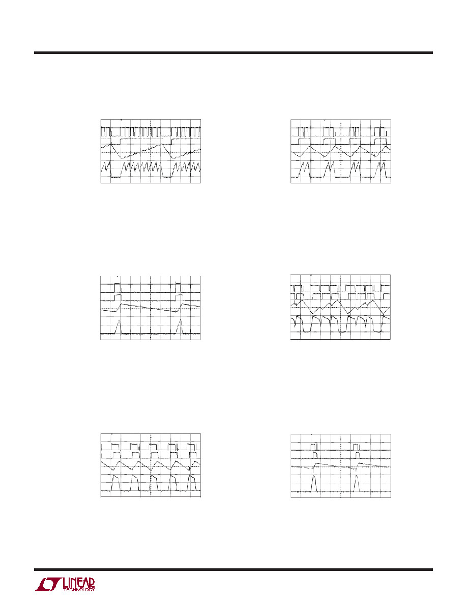
Buck Mode at 5V
IN
,
3.3V
OUT
200mA
Buck Mode at 5V
IN
,
3.3V
OUT
100mA
Buck Mode Waveforms at 5V
IN
,
3.3V
OUT
20mA
3531 G13
3531 G14
3531 G15
SW1
5V/DIV
SW2
5V/DIV
V
OUT
(AC)
50mV/DIV
I
L
200mA/DIV
L = 10H
C
OUT
= 22F
SW1
5V/DIV
SW2
5V/DIV
V
OUT
(AC)
50mV/DIV
I
L
200mA/DIV
SW1
5V/DIV
SW2
5V/DIV
V
OUT
(AC)
50mV/DIV
I
L
200mA/DIV
L = 10H
C
OUT
= 22F
L = 10H
C
OUT
= 22F
TYPICAL PERFOR A CE CHARACTERISTICS
U
W
4 Switch Mode Waveforms at
3.6V
IN
, 3.3V
OUT
200mA
3531 G16
SW1
5V/DIV
SW2
5V/DIV
V
OUT
(AC)
50mV/DIV
I
L
200mA/DIV
L = 10H
C
OUT
= 22F
4 Switch Mode Waveforms at
3.6V
IN
, 3.3V
OUT
100mA
4 Switch Mode Waveforms at
3.6V
IN
, 3.3V
OUT
20mA
3531 G17
3531 G18
SW1
SW2
V
OUT
(AC)
I
L
SW1
5V/DIV
SW2
5V/DIV
V
OUT
(AC)
50mV/DIV
I
L
200mA/DIV
SW1
5V/DIV
SW2
5V/DIV
V
OUT
(AC)
50mV/DIV
I
L
200mA/DIV
L = 10H
C
OUT
= 22F
L = 10H
C
OUT
= 22F
5s/DIV
5s/DIV
5s/DIV
5s/DIV
5s/DIV
5s/DIV
LTC3531/
LTC3531-3.3/LTC3531-3
6
3531f
T
A
= 25∞C unless otherwise specifi ed.
TYPICAL PERFOR A CE CHARACTERISTICS
U
W
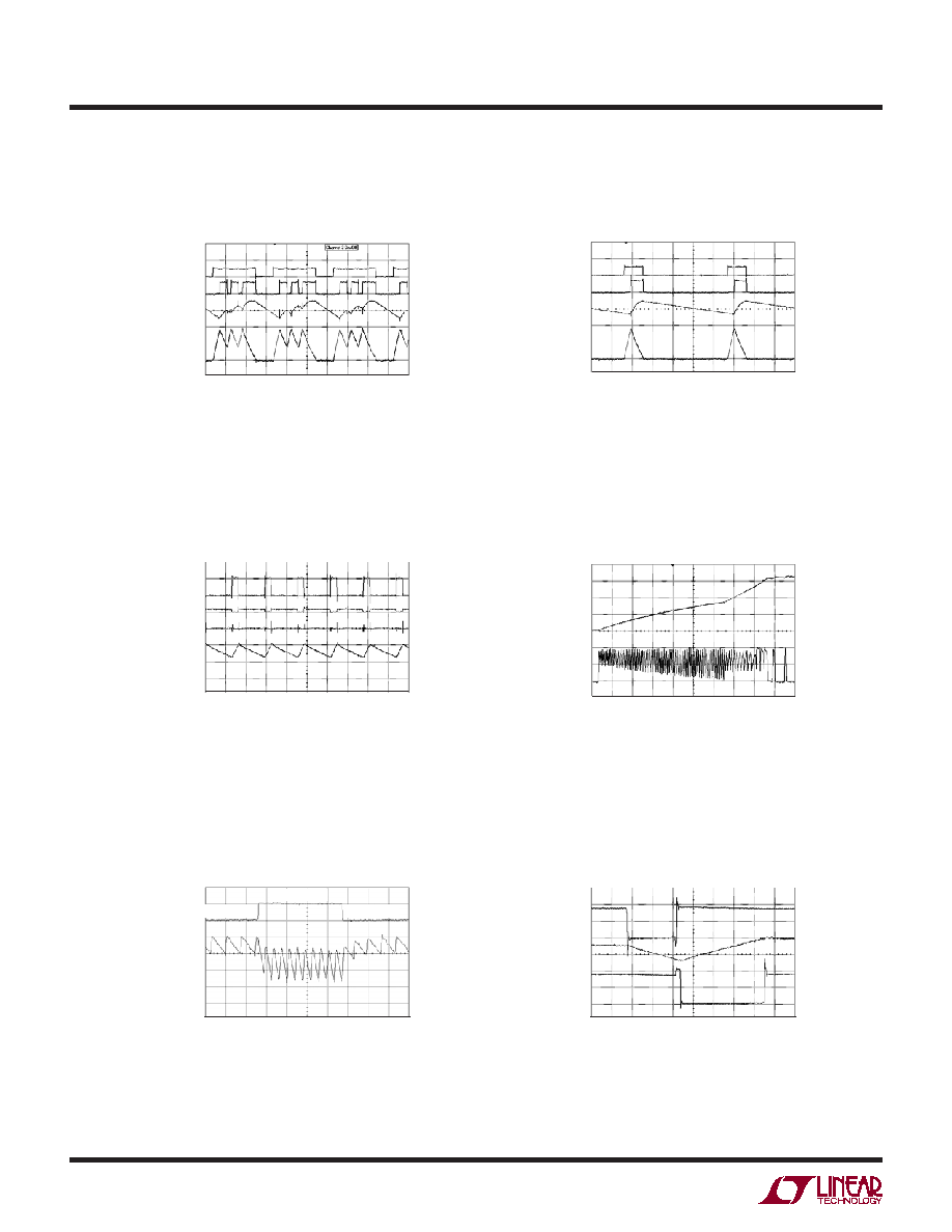
Boost Mode Waveforms at
2.5V
IN
, 3.3V
OUT
100mA
Boost Mode Waveforms at
2.5V
IN
, 3.3V
OUT
20mA
Shorted Output
Start-Up into 50mA Load at
3.3 V
OUT
(Shows Start, Buck,
Then 4sw Modes)
3.6V
IN
, 3.3V
OUT
Load Step
200mA to 80mA
SW1 and SW2 Close-Up in Four
Switch Mode
3531 G22
3531 G23
3531 G24
3531 G19
3531 G20
3531 G21
V
OUT
1V/DIV
I
L
200mA/DIV
SW1
2V/DIV
I
L
200mA/DIV
SW2
2V/DIV
20mA LOAD
100mA LOAD
20mA LOAD
SW1
5V/DIV
SW2
5V/DIV
V
OUT
(AC)
50mV/DIV
I
L
200mA/DIV
L = 10H
C
OUT
= 22F
SW1
5V/DIV
SW2
5V/DIV
V
OUT
(AC)
50mV/DIV
I
L
200mA/DIV
SW1
5V/DIV
SW2
5V/DIV
V
OUT
(AC)
50mV/DIV
I
L
200mA/DIV
L = 10H
C
OUT
= 22F
L = 10H
C
OUT
= 22F
V
IN
= 5
V
OUT
(AC)
20mV/DIV
5s/DIV
5s/DIV
1s/DIV
25s/DIV
25s/DIV
200ns/DIV
200mA/DIV
C
OUT
= 22F
V
IN
= 3.6V
V
OUT
= 3.3V

LTC3531/
LTC3531-3.3/LTC3531-3
7
3531f
PI FU CTIO S
U
U
U
ThinSOT/DFN Packages
SW2 (Pin 1/Pin 7): Buck-Boost Switch Pin Where Internal
Switches C and D are Connected. An optional Schottky
diode can be connected from SW2 to V
OUT
for a moderate
effi ciency improvement. Minimize trace length to keep
EMI down.
GND (Pin 2/Pin 3): Signal Ground for the IC.
PGND (Pin 2/Pin 8): Power Ground for the IC. (Shared
on ThinSOT version)
V
OUT
(Pin 3/Pin 6): Output of the Buck-Boost Synchronous
Rectifi er. A fi lter capacitor is placed from V
OUT
to GND.
A ceramic bypass capacitor is recommended as close to
the V
OUT
and GND pins as possible.
SHDN (Pin 4/Pin 4): External Shutdown Pin. An applied
voltage of < 0.4V shuts down the converter. A voltage
above >1.4V will enable the converter.
V
IN
(Pin 5/Pin 2): Input Supply Pin for the Buck-Boost
Converter. A minimum 2.2µF Ceramic Capacitor should
be placed between V
IN
and GND.
FB (NA/Pin 5): Feedback Pin for the Adjustable Version.
Connect the resistor divider tap here. The output voltage
can be adjusted from 2V to 5V.
V
R
R
OUT
=
+
1 225 1
2
1
.
SW1 (Pin 6/Pin 1): Buck-Boost Switch Pin Where Internal
Switches A and B are Connected. Connect the inductor
from SW1 to SW2.
Exposed Pad (Pin 9, DFN): Solder to PCB ground for
optimal thermal performance.
LTC3531/
LTC3531-3.3/LTC3531-3
8
3531f
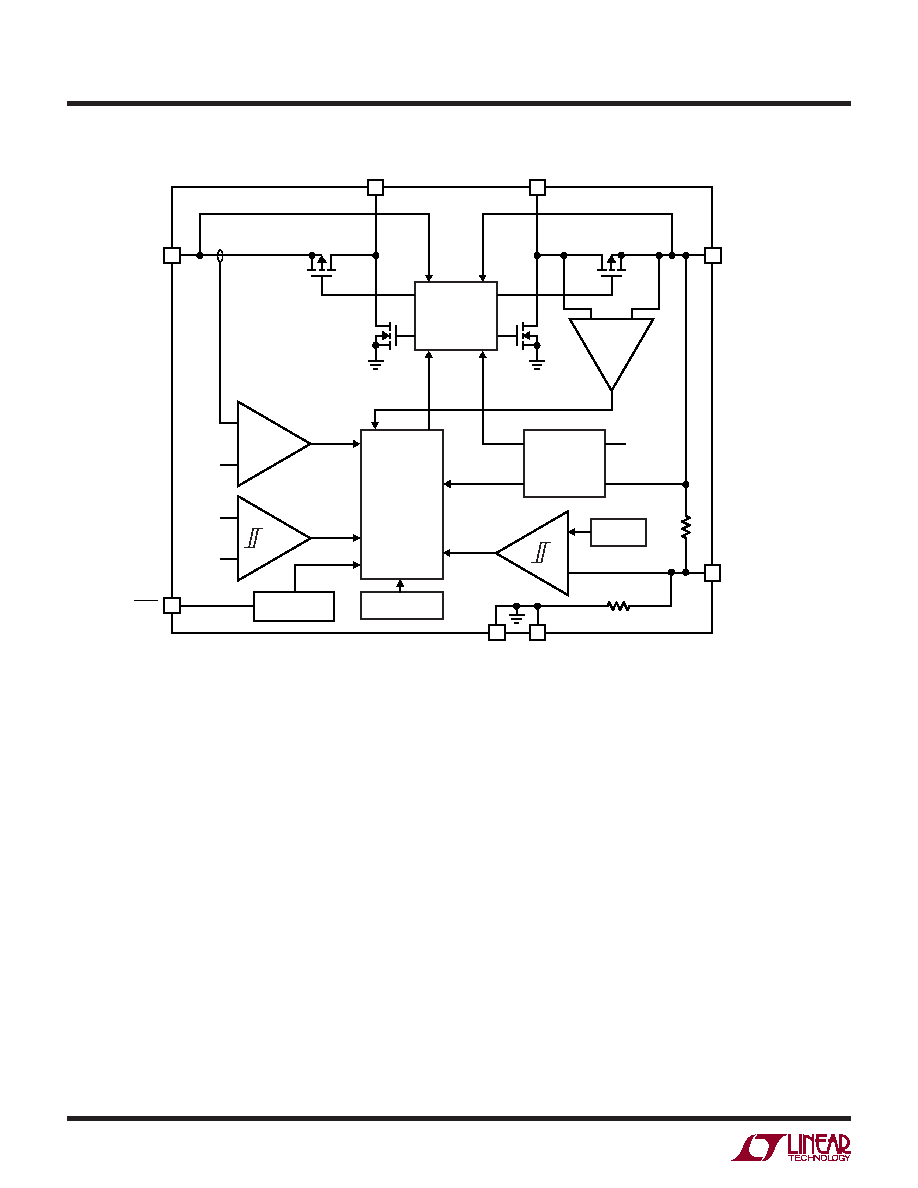
BLOCK DIAGRA
W
3531 BD
GATE DRIVERS
AND
ANTICROSS
CONDUCTION
SHUTDOWN
THERMAL
SHUTDOWN
STATE
MACHINE
AND
LOGIC
V
BEST
AND
MODE DETECT
365mA
V
IN
V
IN
SHDN
PGND
V
OUT
FB
GND
V
IN
V
OUT
1.65V
PEAK
CURRENT
LIMIT
UVLO
V
OUT
COMPARATOR
V
BEST
BUCK, 4SW,
BOOST
I
ZERO
/I
VALLEY
DETECT
SW A
SW1
SW2
SW B
SW C
SW D
1.225V V
REF
NOT BONDED
FOR 3.3V AND
3V VERSIONS
INTERNAL
R1s AND R2s
DISABLED
FOR ADJ VERSION
COMBINED
FOR TSOT
R2
R1
LTC3531/
LTC3531-3.3/LTC3531-3
9
3531f
The LTC3531, LTC3531-3.3 and LTC3531-3 synchro-
nous buck-boost converters utilize a Burst Mode control
technique to achieve high effi ciency over a wide dynamic
range of load currents. A 2% accurate comparator is
used to monitor the output voltage. If V
OUT
is above its
programmed reference threshold no switching occurs and
only quiescent current is drawn from the power source
(sleep mode). When V
OUT
drops below the reference
threshold the IC "wakes up", switching commences, and
the output capacitor is charged. The value of the output
capacitor, the load current, and the comparator hysteresis
(~1%) determines the number of current pulses required
to pump-up the output capacitor before the part returns
to sleep.
In order to determine the best operating mode for the
converter, the LTC3531 contains a second comparator
that monitors the relative voltage difference between V
IN
and V
OUT
. Input and output voltages in the various modes
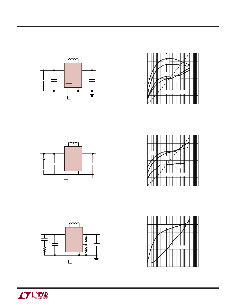
as well as typical inductor currents are shown in Figure 1.
Regions of the current waveforms where switches A and
D are on provide the highest effi ciency since energy is
transferred directly from the input source to the output.
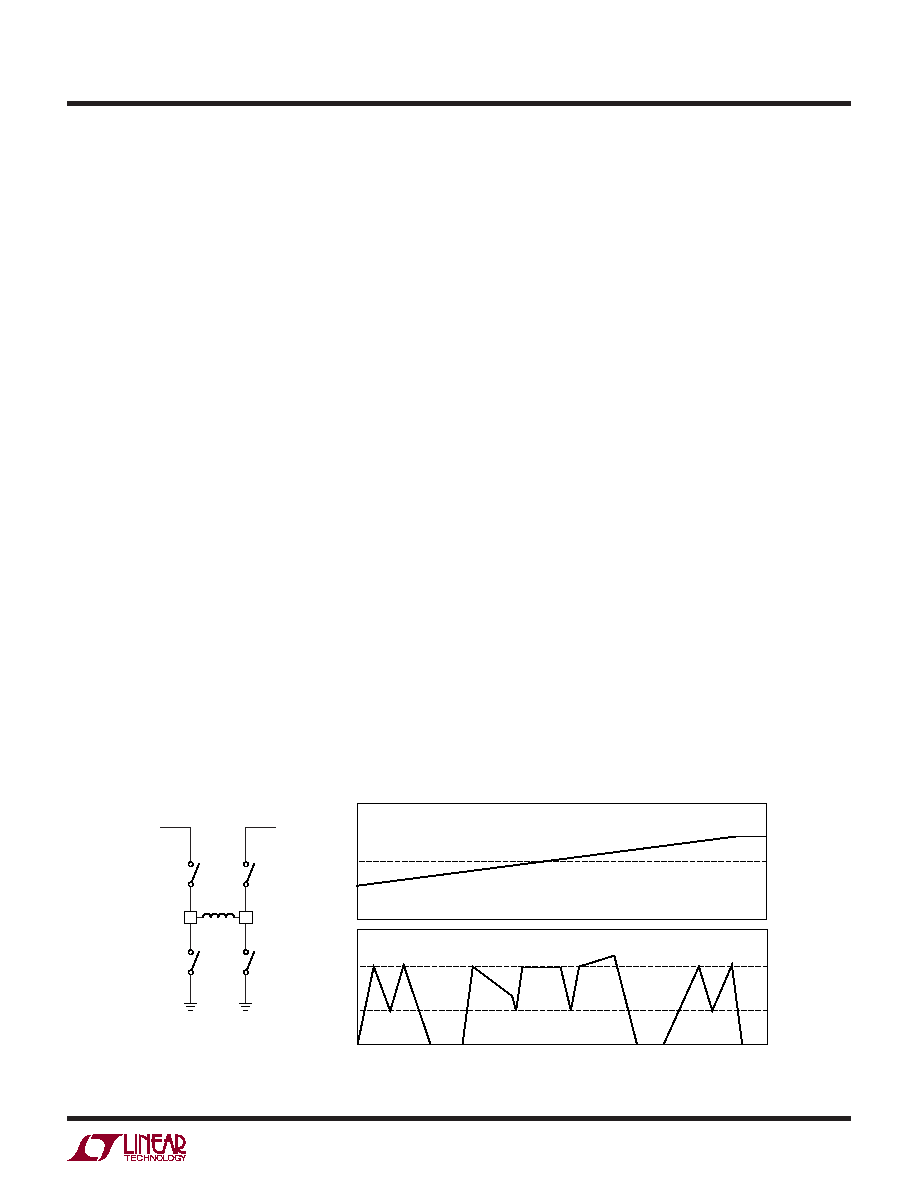
Boost Mode
If V
IN
is ~400mV below V
OUT
, the LTC3531 operates in
boost or step-up mode. Referring to Figure 1 (left side)
when V
OUT
falls below its regulation voltage, switches A
and C are turned on (V
IN
is applied across the inductor)
and current is ramped until I
PEAK
is detected. When this
occurs, C is turned off, D is turned on and current is deliv-
ered to the output capacitor (V
IN
≠ V
OUT
is applied across
the inductor). Inductor current falls when D is on, until an
I
VALLEY
is detected. Terminating at I
VALLEY
, rather than I
ZERO
,
results in an increased load current capability for a given
peak current. This AC then AD switch sequence is repeated
until the output is pumped above its regulation voltage, a
fi nal I
ZERO
is detected, and the part returns to sleep mode
(I
VALLEY
is ignored and I
ZERO
is used in all modes once
V
OUT
is above its programmed value).
4-Switch Mode
If (V
OUT
≠ 400mV) < ~V
IN
< (V
OUT
+ 800mV), the LTC3531
operates in 4-switch step-up/down mode. Returning to
Figure 1 (center) when V
OUT
falls below its regulation volt-
age, switches A and C are turned on and current is ramped
until I
PEAK
is detected. As with Boost Mode operation, C
is then turned off, D is turned on and current is delivered
to the output. When A and D are on, the inductor current
slope is dependant on the relationship between V
IN
, V
OUT
,
and the R
DSON
of the switches. In 4-switch mode, a t
OFF
timer (approximately 3µs) is used to terminate the AD
pulse. Once the t
OFF
timer expires, switch A is turned off,
B is turned on and inductor current is ramped down (V
OUT
is applied across the inductor) until I
VALLEY
is detected.
This sequence is repeated until the output is regulated,
BD switches are turned on, and a fi nal I
ZERO
is detected.
Anticross conduction circuitry in all modes ensures the
P-channel MOSFET and N-channel MOSFET switch pairs (A
and B or D and C) are never turned on simultaneously.
OPERATIO
U
Figure 1. Voltage and Current Waveforms
V
OUT
I
MAX
BOOST MODE
4SW MODE
BUCK MODE
I
PEAK
I
VALLEY
I
ZERO
V
IN
V
IN
t
OFF
t
OFF
t
OFF
AC
AC
AC
AD
AD
AD
AD
AD
AD
AD
AC
AC
BD
BD
BD
BD
BD
3531 F01
V
IN
V
OUT
A
B
C
D
SW1
SW2
L

LTC3531/
LTC3531-3.3/LTC3531-3
10
3531f
Buck Mode
If V
IN
is ~800mV above V
OUT
, the LTC3531 operates in
buck or step-down mode. The higher offset between V
IN
and V
OUT
(800mV) is required to ensure suffi cient mag-
netizing voltage across the inductor when the R
DSONS
are taken into account. At the beginning of a buck mode
cycle (Figure 1 right side) switches A and D are turned
on (V
IN
≠ V
OUT
is applied across the inductor), current
is delivered to the output and ramped up until I
PEAK
is
detected. When this occurs, A is turned off, B is turned
on and inductor current falls (≠V
OUT
across the induc-
tor) until an I
VALLEY
is detected. This AD then BD switch
sequence is repeated until the output is pumped above
its regulation voltage, a fi nal I
ZERO
is detected, and the
part returns to sleep mode.
Start-Up Mode
Before V
OUT
reaches approximately 1.6V, the D switch is
disabled and its body diode is used to transfer current to
the output capacitor. In start-up mode, the I
VALLEY
/I
ZERO
sense circuit is disabled and an alternate algorithm is used
to control inductor current. When the LTC3531 is brought
out of shutdown (assuming V
OUT
is discharged) switches
A and C are turned on until the inductor current reaches
I
PEAK
. The AC switches are then turned off and inductor
current fl ows to the output through the B switch and D
body diode. The period for the B switch/D body diode is
controlled by the t
OFF
timer to ~800nS. This sequence of
AC switch-on to I
PEAK
then B switch and D body diode for
~800ns is repeated until V
OUT
reaches ~1.6V. Once this
OPERATIO
U
threshold is reached, the LTC3531 will transfer through the
required modes until V
OUT
is brought into regulation.
Due to propagation delays in the sense circuitry, the
magnitudes of the I
PEAK
, I
VALLEY
, and I
ZERO
currents may
shift depending on V
IN
, V
OUT
and operating mode.
OTHER LTC3531 FEATURES
Shutdown: The part is shut down by pulling SHDN below
0.4V, and made active by pulling the pin up to V
IN
or V
OUT
.
Note that SHDN can be driven above V
IN
or V
OUT
, as long
as it is limited to less than 6V.
Output Disconnect and Inrush Limiting: The LTC3531
is designed to allow true output disconnect by opening
both P-channel MOSFET rectifi ers. This allows V
OUT
to go
to zero volts during shutdown, drawing no current from
the input source. It also provides inrush current limiting
at turn-on, minimizing surge currents seen by the input
supply.
Thermal Shutdown: If the die temperature reaches ap-
proximately 150∞C, the part will go into thermal shut-
down and all switches will be turned off. The part will be
enabled again when the die temperature has dropped by
10∞C (nominal). To deliver the power that the LTC3531
is capable of, it is imperative that a good thermal path be
provided to dissipate the heat generated within the pack-
age. It is recommended that multiple vias in the printed
circuit board be used to conduct heat away from the IC
and into a copper plane with as much area as possible.
Soldering the Exposed Pad to the GND plane (DFN version)
is recommended to improve thermal performance.
LTC3531/
LTC3531-3.3/LTC3531-3
11
3531f
S I FOR ATIO
APPLICATIO
W
U
U
U
Table 3. Capacitor Vendor Information
Supplier Series
Phone
Website
AVX X5R
(803)
448-9411
www.avxcorp.com
Murata
X5R
USA: (814) 237-1431 www.murata.com
(800)
831-9172
Sanyo POSCAP
(619)
661-6322 www.sanyovideo.com
Taiyo Yuden X5R
(408) 573-4150
www.taiyo-yuden.com
TDK X5R
(847)
803-6100
www.component.tdk.com
Component Selection
Only three power components are required to
complete the design of the buck-boost converter, V
OUT
programming resistors are needed for the adjustable
version. The high operating frequency and low peak
currents of the LTC3531 allow the use of low value, low
profi le inductors and tiny external ceramic capacitors.
Inductor Selection
For best effi ciency, choose an inductor with high frequency
core material, such as ferrite, to reduce core loses. The
inductor should have low DCR (DC resistance) to reduce
the I
2
R losses, and must be able to handle the peak
inductor current without saturating. A 10µH to 22µH in-
ductor value with a >500mA current rating and <400m
DCR is recommended. For applications where radiated
noise is a concern, a toroidal or shielded inductor can be
used. Table 2 contains a list of inductor manufacturers.
Capacitor Selection
The buck-boost convertor requires two capacitors. Ceramic
X5R types will minimize ESL and ESR while maintaining
capacitance at rated voltage over temperature. The V
IN
capacitor should be at least 2.2µF. The V
OUT
capacitor
should be between 4.7µF and 22µF. A larger output capaci-
tor should be used if lower peak to peak output voltage
ripple is desired. A larger output capacitor will also improve
load regulation on V
OUT
. See Table 3 for a list of capacitor
manufacturers for input and output capacitor selection.
Table 2. Inductor Vendor Information
Supplier Series
Phone
Website
COEV DN4835
(800)
227-7040
www.coev.net
Coilcraft MSS4020
(847)
639-6400
www.coilcraft.com
LPO3310
DS1608
Murata LQH43CN
USA:
(814)
237-1431 www.murata.com
LQH32CN
(800)
831-9172
Sumida CDRH4D18
USA:
(847)
956-0666 www.sumida.com
CDRH3D16/HP
Japan:
81-3-3607-5111
Toko D312C
(847)
297-0070
www.tokoam.com
D412C
DB320C
LTC3531/
LTC3531-3.3/LTC3531-3
12
3531f
S I FOR ATIO
APPLICATIO
W
U
U
U
5 ≠ V
IN
V
OUT
≠ 3
V
IN
C
IN
V
OUT
C
OUT
GND
GND
GND ≠ 2
SHUTDOWN
L
4 ≠ SHDN
6 ≠ SW1
SW2 ≠ 1
SOT PIN-OUT
Recommended Layout (SOT Versions)
LTC3531/
LTC3531-3.3/LTC3531-3
13
3531f
5V/Li-Ion to 3.3V with ThinSOT (3.3V Version)
2 AA Alkaline to 3V with ThinSOT (3V Version)
TYPICAL APPLICATIO S
U
SW1
SW2
SHDN
GND
V
IN
V
OUT
LTC3531-3.3
+
≠
2.2
µF
10
µF
5V/Li-Ion
ON OFF
10
µH
V
OUT
3.3V
160mA
V
IN
3.1V TO
5V
3531 TA02a
LOAD CURRENT (mA)
75
EFFICIENCY (%)
85
95
70
80
90
0.1
10
100
1000
3531 TA02b
65
1
4.4V
IN
5V
IN
3.6V
IN
3.1V
IN
POWER LOSS AT 3.6V
IN
POWER LOSS (mW)
0.1
10
1
100
SW1
SW2
SHDN
GND
V
IN
V
OUT
LTC3531-3
+
≠
2.2
µF
10
µF
+
≠
2 x AA
ALKALINE
ON OFF
10
µH
3531 TA03a
V
OUT
3V
80mA
V
IN
1.8V TO
3.2V
LOAD CURRENT (mA)
70
EFFICIENCY (%)
80
90
65
75
85
0.1
10
100
1000
3531 TA03b
60
1
2.5V
IN
3.2V
IN
POWER LOSS AT 3.2V
IN
1.8V
IN
POWER LOSS (mW)
0.1
10
1
100
SW1
SW2
SHDN
GND
V
IN
V
OUT
FB
LTC3531
2.2
µF
10
µF
R2
1M
R1
324k
4.7
µF
ON OFF
10
µH
3531 TA04a
1
V
OUT
5V
200mA
USB
4.35V TO
5.25V
LOAD CURRENT (mA)
75
EFFICIENCY (%)
POWER LOSS (mW)
85
95
70
80
90
0.1
10
100
1000
3531 TA04b
65
0.1
10
1
100
1
EFFICIENCY
POWER LOSS
USB to 5V with 3 ◊ 3 DFN (Adjustable Version)
LTC3531/
LTC3531-3.3/LTC3531-3
14
3531f
PACKAGE DESCRIPTIO
U
S6 Package
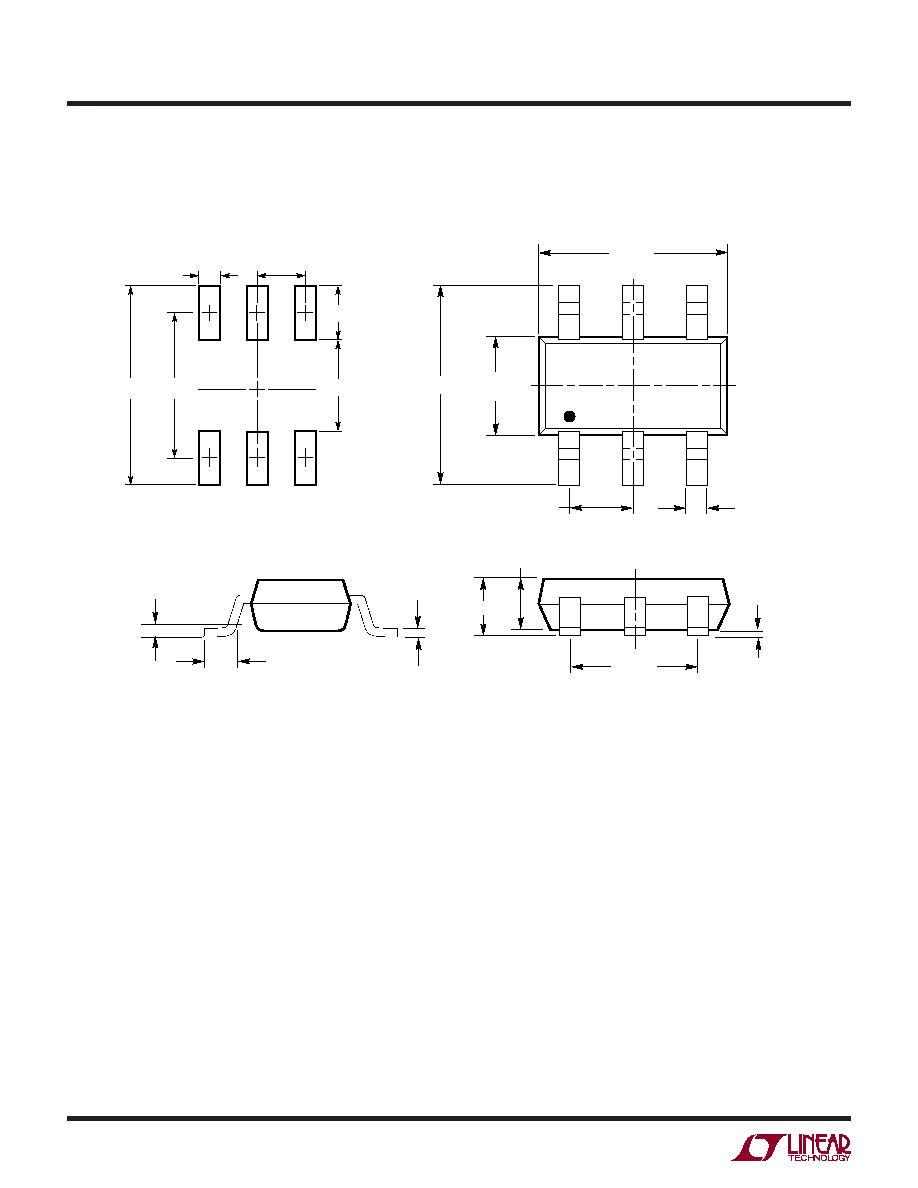
6-Lead Plastic TSOT-23
(Reference LTC DWG # 05-08-1636)
1.50 ≠ 1.75
(NOTE 4)
2.80 BSC
0.30 ≠ 0.45
6 PLCS (NOTE 3)
DATUM `A'
0.09 ≠ 0.20
(NOTE 3)
S6 TSOT-23 0302
2.90 BSC
(NOTE 4)
0.95 BSC
1.90 BSC
0.80 ≠ 0.90
1.00 MAX
0.01 ≠ 0.10
0.20 BSC
0.30 ≠ 0.50 REF
PIN ONE ID
NOTE:
1. DIMENSIONS ARE IN MILLIMETERS
2. DRAWING NOT TO SCALE
3. DIMENSIONS ARE INCLUSIVE OF PLATING
3.85 MAX
0.62
MAX
0.95
REF
RECOMMENDED SOLDER PAD LAYOUT
PER IPC CALCULATOR
1.4 MIN
2.62 REF
1.22 REF
4. DIMENSIONS ARE EXCLUSIVE OF MOLD FLASH AND METAL BURR
5. MOLD FLASH SHALL NOT EXCEED 0.254mm
6 JEDEC PACKAGE REFERENCE IS MO-193
LTC3531/
LTC3531-3.3/LTC3531-3
15
3531f
Information furnished by Linear Technology Corporation is believed to be accurate and reliable. However,
no responsibility is assumed for its use. Linear Technology Corporation makes no representation that
the interconnection of its circuits as described herein will not infringe on existing patent rights.
DD Package
8-Lead Plastic DFN (3mm ◊ 3mm)
(Reference LTC DWG # 05-08-1698)
PACKAGE DESCRIPTIO
U
3.00
±0.10
(4 SIDES)
NOTE:
1. DRAWING TO BE MADE A JEDEC PACKAGE OUTLINE
M0-229 VARIATION OF (WEED-1)
2. DRAWING NOT TO SCALE
3. ALL DIMENSIONS ARE IN MILLIMETERS
0.38
± 0.10
BOTTOM VIEW--EXPOSED PAD
1.65
± 0.10
(2 SIDES)
0.75
±0.05
R = 0.115
TYP
2.38
±0.10
(2 SIDES)
1
4
8
5
PIN 1
TOP MARK
(NOTE 6)
0.200 REF
0.00 ≠ 0.05
(DD8) DFN 1203
0.25
± 0.05
2.38
±0.05
(2 SIDES)
RECOMMENDED SOLDER PAD PITCH AND DIMENSIONS
1.65
±0.05
(2 SIDES)
2.15
±0.05
0.50
BSC
0.675
±0.05
3.5
±0.05
PACKAGE
OUTLINE
0.25
± 0.05
0.50 BSC
4. DIMENSIONS OF EXPOSED PAD ON BOTTOM OF PACKAGE DO NOT INCLUDE
MOLD FLASH. MOLD FLASH, IF PRESENT, SHALL NOT EXCEED 0.15mm ON ANY SIDE
5. EXPOSED PAD SHALL BE SOLDER PLATED
6. SHADED AREA IS ONLY A REFERENCE FOR PIN 1 LOCATION
ON TOP AND BOTTOM OF PACKAGE
LTC3531/
LTC3531-3.3/LTC3531-3
16
3531f
Linear Technology Corporation
1630 McCarthy Blvd., Milpitas, CA 95035-7417
(408) 432-1900
FAX: (408) 434-0507
www.linear.com
© LINEAR TECHNOLOGY CORPORATION 2005
LT 1105 ∑ PRINTED IN USA
TYPICAL APPLICATIO S
U
SW1
SW2
SHDN
GND
V
IN
V
OUT
LTC3531-3.3
C2
10
µF
C1
22
µF
L1
10
µH
3.1V TO 5.25V
3531 TA05
OTHER
DC/DC
100k
100k
0.1
µF
SHDN WALL NTC
OUT
CHRG
ACPR
VNTC
TIMER
CLPROG
PROG
IN1
IN2
HPWR
SUSP
BAT
GND
LTC4055
+
≠
Li-Ion
5V (NOM)
FROM USB
CABLE
SUSPEND
USB POWER
V
OUT
: USB OR BATTERY
C1, C2: TAIYO YUDEN JMK316BJ106ML
L1: MURATA LQH43CN100K03 (650mA 0.24
)
V
OUT
3.3V
160mA
Complete USB/Li-Ion Powered System
with 3.3V
OUT
and Linear Charger
RELATED PARTS
PART NUMBER
DESCRIPTION
COMMENTS
LT1930/LT1930A 1A
(I
SW
), 1.2MHz/2.2MHz, High Effi ciency Step-Up DC/DC Converter
V
IN
: 2.6V to 16V, V
OUT(MAX)
= 34V,
I
Q
= 4.2mA/5.5mA, I
SD
< 1µA, ThinSOT Package
LTC3400/LTC3400B 600mA
(I
SW
), 1.2MHz Synchronous Step-Up DC/DC Converter
V
IN
: 0.85V to 5V, V
OUT(MAX)
= 5V,
I
Q
= 19µA/300µA, I
SD
< 1µA, ThinSOT Package
LTC3401/LTC3402 1A/2A
(I
SW
), 3MHz Synchronous Step-Up DC/DC Converter
V
IN
: 0.5V to 5V, V
OUT(MAX)
= 6V, I
Q
= 38µA,
I
SD
< 1µA, MS Package
LTC3405/LTC3405A 300mA
(I
OUT
), 1.5MHz Synchronous Step-Down DC/DC Converter
V
IN
: 2.7V to 6V, V
OUT(MIN)
= 0.8V, I
Q
= 20µA,
I
SD
1µA, MS10 Package
LTC3406/LTC3406B 600mA
(I
OUT
), 1.5MHz Synchronous Step-Down DC/DC Converter
V
IN
: 2.5V to 5.5V, V
OUT(MIN)
= 0.6V, I
Q
= 20µA,
I
SD
1µA, ThinSOT Package
LTC3421 3A
(I
SW
), 3MHz Synchronous Step-Up DC/DC Converter
V
IN
: 0.5V to 4.5V, V
OUT(MAX)
= 5.25V, I
Q
= 12µA,
I
SD
< 1µA, QFN Package
LTC3422 1.5A
(I
SW
), 3MHz Synchronous Step-Up DC/DC Converter
V
IN
: 0.5V to 4.5V, V
OUT(MAX)
= 5.25V, I
Q
= 25µA,
I
SD
< 1µA, 3mm ◊ 3mm DFN Package
LTC3426 2A
(I
SW
), 1.2MHz Step-Up DC/DC Converter in SOT-23
V
IN
: 1.6V to 5V, V
OUT
up to 5.5V
LTC3428 4A
(I
SW
), 1.2MHz Step-Up DC/DC Converter
V
IN
: 1.6V to 5V, V
OUT
up to 5.5V
LTC3429 600mA
(I
SW
), 500kHz Synchronous Step-Up DC/DC Converter
V
IN
: 0.5V to 4.4V, V
OUT(MIN)
= 5V, I
Q
= 20µA,
I
SD
< 1µA, QFN Package
LTC3440 600mA
(I
OUT
), 2MHz Synchronous Buck-Boost DC/DC Converter
V
IN
: 2.5V to 5.5V, V
OUT(MIN)
= 5.5V, I
Q
= 25µA,
I
SD
< 1µA, MS, DFN Packages
LTC3441 600mA
(I
OUT
), 2MHz Synchronous Buck-Boost DC/DC Converter
V
IN
: 2.5V to 5.5V, V
OUT(MIN)
= 5.5V, I
Q
= 25µA,
I
SD
< 1µA, DFN Package
LTC3442
2MHz Synchronous Buck-Boost with Auto-Burst
V
IN
: 2.4V to 5.5V, V
OUT
up to 5.25V
LTC3443 1.2A
(I
OUT
), 600kHz Synchronous Buck-Boost DC/DC Converter
V
IN
: 2.4V to 5.5V, V
OUT(MIN)
= 5.25V, I
Q
= 28µA,
I
SD
< 1µA, MS Package
LTC3458
1.4A, 1.5MHz Synchronous Step-Up DC/DC Converter
V
IN
: 1.5V to 6V, V
OUT
up to 7.5V
LTC3458L
1.7A, 1.5MHz Synchronous Step-Up DC/DC Converter
V
IN
: 1.5V to 6V, V
OUT
up to 6V
LTC3459
10V Micropower Synchronous Step-Up DC/DC Converter
V
IN
: 1.5V to 5.5V, V
OUT
up to 10V
LTC3525/LTC3525-3.3/ 400mA
(I
SW
), Synchronous Step-Up DC/DC Converter
V
IN
: 0.5V to 4.5V, I
Q
= 7µA, I
SD
< 1µA,
LTC3525-5 with
Output
Disconnect
2mm
◊ 2mm SC70 Package