 | ÐлекÑÑоннÑй компоненÑ: LTC3550-1 | СкаÑаÑÑ:  PDF PDF  ZIP ZIP |
3550-1.indd
LTC3550-1
1
35501f
TIME (HR)
0
CHARGE
CURRENT (mA)
BATTERY
VOLTAGE (V)
DCIN
VOLTAGE (V)
4.2
200
0
400
800
600
1000
1.5
2.5
3550-1 TA02
3.6
3.4
5.0
4.0
3.8
2.5
0
2.5
0.5
1.0
2.0
3.0
CONSTANT VOLTAGE
USBIN = 5V
T
A
= 25
°C
R
IDC
= 1.25k
R
IUSB
= 2k
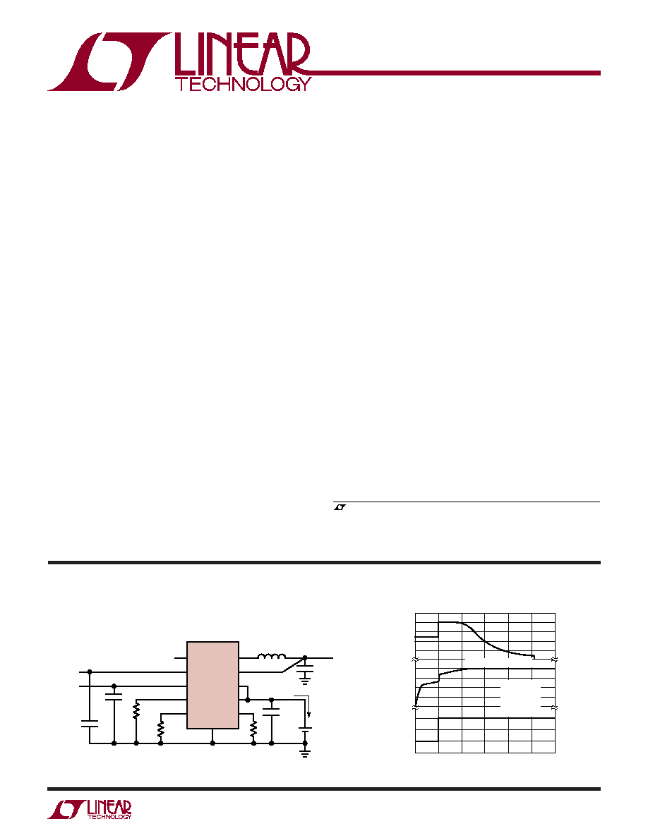
Dual Input USB/AC Adapter
Li-Ion Battery Charger with
600mA Buck Converter
The LTC
®
3550-1 is a standalone linear charger with a
600mA monolithic synchronous buck converter. It is
capable of charging a single-cell Li-Ion battery from both
wall adapter and USB inputs. The charger automatically
selects the appropriate power source for charging.
Internal thermal feedback regulates the battery charge
current to maintain a constant die temperature during high
power operation or high ambient temperature conditions.
The fl oat voltage is fi xed at 4.2V and the charge currents
are programmed with external resistors. The LTC3550-1
terminates the charge cycle when the charge current drops
below the programmed termination threshold after the
fi nal fl oat voltage is reached. With power applied to both
inputs, the LTC3550-1 can be put into shutdown mode
reducing the DCIN supply current to 20A, the USBIN
supply current to 10A, and the battery drain current to
less than 2A.
The synchronous buck converter generates a fi xed output
voltage of 1.875V. The switching frequency is internally
set at 1.5MHz, allowing the use of small surface mount
inductors and capacitors.
Cellular Telephones
Charges Single-Cell Li-Ion Batteries from Wall
Adapter and USB Inputs
Automatic Input Power Detection and Selection
Charge Current Programmable Up to 950mA from
Wall Adapter Input
High Effi ciency 600mA Synchronous DC/DC
Converter
No External MOSFET, Sense Resistor or Blocking
Diode Needed
Thermal Regulation Maximizes Charge Rate Without
Risk of Overheating*
Preset Charge Voltage with ±0.6% Accuracy
Programmable Charge Current Termination
1.5MHz Constant Frequency Operation (Step-Down
Converter)
18A USB Suspend Current in Shutdown
Independent "Power Present" Status Outputs
Charge Status Output
Automatic Recharge
Available in a Thermally Enhanced, Low Profi le
(0.75mm) 16-Lead (5mm x 3mm) DFN Package
APPLICATIO S
U
FEATURES
DESCRIPTIO
U
TYPICAL APPLICATIO
U
, LTC and LT are registered trademarks of Linear Technology Corporation.
All other trademarks are the property of their respective owners.
*Protected by U.S. patents, includng 6522118, 6700364, 6580258, 5481178, 6304066,
6127815, 6498466, 6611131
Complete Charge Cycle (1100mA Battery)
Dual Input Battery Charger and DC/DC Converter
1.24k
1%
2k
1%
WALL
ADAPTER
USB
PORT
1
µF
1
µF
3550-1 TA01
4.7
µF
LTC3550-1
RUN
DCIN
USBIN
IUSB
IDC
SW
V
OUT
V
CC
BAT
GND
C
OUT
10
µF
CER
ITERM
+
2.2
µH
4.2V
SINGLE-CELL
Li-Ion BATTERY
V
OUT
1.875V
600mA
2k
1%
800mA (WALL)
500mA (USB)
LTC3550-1
2
35501f
DCIN, USBIN .............................................. 0.3V to 10V
ENABLE,
C
H
R
G,
P
W
R, USBPWR ............... 0.3V to 10V
BAT, IDC, IUSB, ITERM ................................ 0.3V to 7V
V
CC
............................................................... 0.3V to 6V
RUN, V
OUT
..................................................0.3V to V
CC
SW (DC) ........................................ 0.3V to (V
CC
+ 0.3V)
DCIN Pin Current (Note 2) ..........................................1A
USBIN Pin Current (Note 2) .................................700mA
BAT Pin Current (Note 2) ............................................1A
P-Channel SW Source Current (DC) .....................800mA
N-Channel SW Source Current (DC) ....................800mA
Peak SW Sink and Source Current ...........................1.3A
Operating Temperature Range (Note 3) ... 40°C to 85°C
Maximum Junction Temperature .......................... 125°C
Storage Temperature Range ................... 65°C to 125°C
(Note 1)
The
denotes the specifi cations which apply over the full operating
temperature range, otherwise specifi cations are at T
A
= 25°C. V
DCIN
= 5V, V
USBIN
= 5V, V
CC
= 3.6V unless otherwise noted.
SYMBOL
PARAMETER
CONDITIONS
MIN
TYP
MAX
UNITS
V
DCIN
Wall Adapter Input Supply Voltage
4.3
8
V
V
USBIN
USB Port Input Supply Voltage
4.3
8
V
V
CC
Buck Regulator Input Supply Voltage
2.5
5.5
V
V
ENABLE
ENABLE Input Threshold Voltage
0.4
0.7
1.0
V
R
ENABLE
ENABLE Pulldown Resistance
1.2
2
5
M
V
RUN
RUN Threshold Voltage
0.3
1
1.5
V
I
RUN
RUN Leakage Current
±0.01
±1
µA
V
CHRG
C
H
R
G Output Low Voltage
I
CHRG
= 5mA
0.35
0.6
V
V
PWR
P
W
R Output Low Voltage
I
PWR
= 5mA
0.35
0.6
V
V
USBPWR
USBPWR Output Low Voltage
I
USBPWR
= 200µA
0.35
0.6
V
V
UVDC
DCIN Undervoltage Lockout Voltage
From Low to High
Hysteresis
4.0
4.15
200
4.3
V
mV
V
UVUSB
USBIN Undervoltage Lockout Voltage
From Low to High
Hysteresis
3.8
3.95
200
4.1
V
mV
ELECTRICAL CHARACTERISTICS
ABSOLUTE AXI U
RATI GS
W
W
W
U
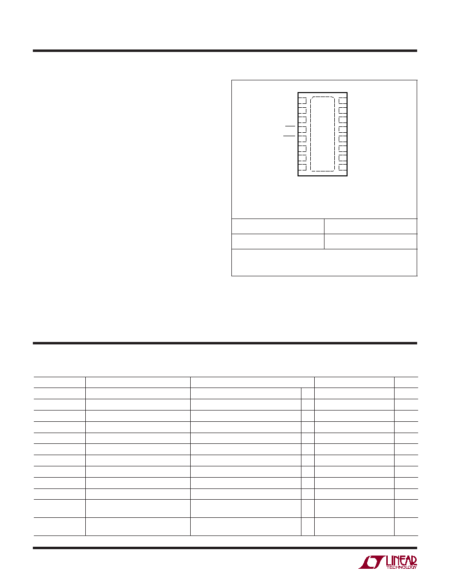
PACKAGE/ORDER I FOR ATIO
U
U
W
16
15
14
13
12
11
10
9
17
1
2
3
4
5
6
7
8
DCIN
BAT
IDC
USBPWR
ENABLE
RUN
SW
GND
USBIN
IUSB
ITERM
PWR
CHRG
V
OUT
V
CC
GND
TOP VIEW
DHC PACKAGE
16-LEAD (5mm
× 3mm) PLASTIC DFN
T
JMAX
= 125°C,
JA
= 40°C (Note 4)
EXPOSED PAD IS GROUND (PIN 17)
MUST BE SOLDERED TO PCB
ORDER PART NUMBER
PART MARKING
LTC3550EDHC-1
35501
Order Options Tape and Reel: Add #TR
Lead Free: Add #PBF Lead Free Tape and Reel: Add #TRPBF
Lead Free Part Marking:
http://www.linear.com/leadfree/
Consult LTC Marketing for parts specifi ed with wider operating temperature ranges.
LTC3550-1
3
35501f
SYMBOL
PARAMETER
CONDITIONS
MIN
TYP
MAX
UNITS
V
ASD-DC
V
DCIN
V
BAT
Lockout Threshold Voltage
V
DCIN
from Low to High, V
BAT
= 4.2V
V
DCIN
from High to Low, V
BAT
= 4.2V
140
20
180
50
220
80
mV
mV
V
ASD-USB
V
USBIN
V
BAT
Lockout Threshold
Voltage
V
USBIN
from Low to High, V
BAT
= 4.2V
V
USBIN
from High to Low, V
BAT
= 4.2V
140
20
180
50
220
80
mV
mV
Battery Charger
I
DCIN
DCIN Supply Current
Charge Mode (Note 5)
Standby Mode
Shutdown Mode
R
IDC
= 10k
Charge Terminated
ENABLE = 5V
250
50
20
800
100
40
µA
µA
µA
I
USBIN
USBIN Supply Current
Charge Mode (Note 6)
Standby Mode
Shutdown Mode
Shutdown Mode
R
IUSB
= 10k, V
DCIN
= 0V
Charge Terminated
V
DCIN
= 0V, ENABLE = 0V
V
DCIN
> V
USBIN
250
50
18
10
800
100
36
20
µA
µA
µA
µA
V
FLOAT
Regulated Output (Float) Voltage
I
BAT
= 1mA
I
BAT
= 1mA, 0°C < T
A
< 85°C
4.175
4.158
4.2
4.2
4.225
4.242
V
V
I
BAT
BAT Pin Current
Constant-Current Mode
Constant-Current Mode
Constant-Current Mode
Standby Mode
Shutdown Mode
Sleep Mode
R
IDC
= 1.25k
R
IUSB
= 2.1k
R
IDC
= 10k or R
IUSB
= 10k
Charge Terminated
Charger Disabled
DCIN
= 0V, USBIN
= 0V
760
450
93
800
476
100
3
1
±1
840
500
107
6
2
±2
mA
mA
mA
µA
µA
µA
V
IDC
IDC Pin Regulated Voltage
Constant-Current Mode
0.95
1.0
1.05
V
V
IUSB
IUSB Pin Regulated Voltage
Constant-Current Mode
0.95
1.0
1.05
V
I
TERMINATE
Charge Current Termination Threshold
R
ITERM
= 1k
R
ITERM
= 2k
R
ITERM
= 10k
R
ITERM
= 20k
90
45
8.5
4
100
50
10
5
110
55
11.5
6
mA
mA
mA
mA
V
RECHRG
Recharge Battery Threshold Voltage
V
FLOAT
V
RECHRG
, 0°C < T
A
< 85°C
65
100
135
mV
t
RECHRG
Recharge Comparator Filter Time
V
BAT
from High to Low
3
6
9
ms
t
TERMINATE
Termination Comparator Filter Time
I
BAT
Drops Below Termination Threshold
0.8
1.5
2.2
ms
t
SS
Soft-Start Time
I
BAT
= 10% to 90% Full-Scale
175
250
325
µs
R
ON-DC
Power FET On-Resistance (Between
DCIN and BAT)
400
m
R
ON-USB
Power FET On-Resistance (Between
USBIN and BAT)
550
m
T
LIM
Junction Temperature in Constant-
Temperature Mode
105
°C
Switching Regulator
V
OUT
Regulated Output Voltage
I
OUT
= 100mA
1.819
1.875
1.931
V
V
OUT
Output Voltage Line Regulation
0.04
0.4
%/V
I
PK
Peak Inductor Current
V
CC
= 3V, V
OUT
= 1.7V
0.75
1
1.25
A
V
LOADREG
Output Voltage Load Regulation
0.5
%
I
S
Input DC Bias Current
Active Mode
Sleep Mode
Shutdown
(Note 7)
V
OUT
= 1.7V, I
LOAD
= 0A
V
OUT
= 1.94V, I
LOAD
= 0A
V
RUN
= 0V, V
CC
= 5.5V
300
20
0.1
400
35
1
µA
µA
µA
The
denotes the specifi cations which apply over the full operating
temperature range, otherwise specifi cations are at T
A
= 25°C. V
DCIN
= 5V, V
USBIN
= 5V, V
CC
= 3.6V unless otherwise noted.
ELECTRICAL CHARACTERISTICS
LTC3550-1
4
35501f
SYMBOL
PARAMETER
CONDITIONS
MIN
TYP
MAX
UNITS
f
OSC
Oscillator Frequency
V
OUT
= 100%
V
OUT
= 0V
1.2
1.5
210
1.8
MHz
kHz
R
PFET
R
DS(ON)
of P-Channel FET
0.4
R
NFET
R
DS(ON)
of N-Channel FET
0.35
I
LSW
SW Leakage Current
0.01
±1
µA
The
denotes the specifi cations which apply over the full operating
temperature range, otherwise specifi cations are at T
A
= 25°C. V
DCIN
= 5V, V
USBIN
= 5V, V
CC
= 3.6V unless otherwise noted.
ELECTRICAL CHARACTERISTICS
Note 1: Stresses beyond those listed under Absolute Maximum Ratings
may cause permanent damage to the device. Exposure to any Absolute
Maximum Rating condition for extended periods may affect device
reliability and lifetime.
Note 2: Guaranteed by long term current density limitations.
Note 3: The LTC3550E-1 is guaranteed to meet the performance
specifi cations from 0°C to 70°C. Specifi cations over the 40°C to 85°C
operating temperature range are assured by design, characterization and
correlation with statistical process controls.
Note 4: Failure to solder the exposed backside of the package to the PC
board will result in a thermal resistance much higher than 40°C/W. See
Thermal Considerations.
Note 5: Supply Current includes IDC and ITERM pin current (approx-
imately 100A each) but does not include any current delivered to the
battery through the BAT pin (approximately 100mA).
Note 6: Supply Current includes IUSB and ITERM pin current (approx-
imately 100A each) but does not include any current delivered to the
battery through the BAT pin (approximately 100mA).
Note 7: Dynamic supply current is higher due to the gate charge being
delivered at the switching frequency.
LTC3550-1
5
35501f
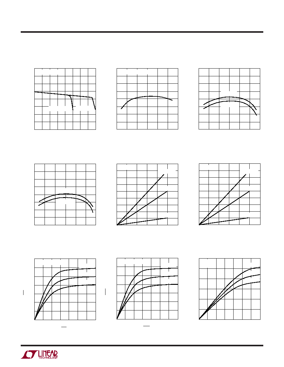
TEMPERATURE (
°C)
50
25
V
FLOAT
(V)
0
50
25
75
100
3550-1 G02
4.220
4.215
4.210
4.205
4.200
4.195
4.190
4.185
4.180
V
DCIN
= V
USBIN
= 5V
CHARGE CURRENT (mA)
0
V
FLOAT
(V)
800
500 600 700
400
3550-1 G01
100 200 300
4.26
4.24
4.22
4.20
4.18
4.16
4.14
4.12
4.10
R
IDC
= 1.25k
R
IDC
= R
IUSB
= 2k
V
DCIN
= V
USBIN
= 5V
TEMPERATURE (
°C)
50
25
0
50
25
75
100
V
IDC
(V)
3550-1 G03
1.008
1.006
1.004
1.002
1.000
0.998
0.996
0.994
0.992
V
DCIN
= 8V
V
DCIN
= 4.3V
3550-1 G04
TEMPERATURE (
°C)
50
25
0
50
25
75
100
V
IUSB
(V)
1.008
1.006
1.004
1.002
1.000
0.998
0.996
0.994
0.992
V
USBIN
= 8V
V
USBIN
= 4.3V
V
IDC
(V)
0
0.2
0.6
1.0
I
BAT
(mA)
0.8
900
800
700
600
500
400
300
200
100
0
3550-1 G05
0.4
1.2
V
DCIN
= 5V
R
IDC
= 1.25k
R
IDC
= 2k
R
IDC
= 10k
I
BAT
(mA)
900
800
700
600
500
400
300
200
100
0
V
IUSB
(V)
0
0.2
0.6
1.0
0.8
0.4
1.2
3550-1 G06
V
USBIN
= 5V
R
IUSB
= 1.25k
R
IUSB
= 2k
R
IUSB
= 10k
V
PWR
(V)
0
35
30
25
20
15
10
5
0
3
5
3550-1 G07
1
2
4
6
7
I
PWR
(mA)
V
DCIN
= V
USBIN
= 5V
T
A
= 40
°C
T
A
= 25
°C
T
A
= 90
°C
3550-1 G08
V
DCIN
= V
USBIN
= 5V
35
30
25
20
15
10
5
0
I
CHRG
(mA)
T
A
= 40
°C
T
A
= 25
°C
T
A
= 90
°C
V
CHRG
(V)
0
3
5
1
2
4
6
7
T
A
= 40
°C
T
A
= 25
°C
T
A
= 90
°C
V
USBPWR
(V)
0
I
USBPWR
(mA)
6
5
4
3
2
1
0
3
5
3550-1 G09
1
2
4
6
7
V
DCIN
= 5V
V
USBIN
= 0V
IUSB Pin Voltage vs Temperature
(Constant-Current Mode)
Charge Current vs IDC Pin Voltage
Charge Current
vs IUSB Pin Voltage
P
W
R Pin I-V Curve
C
H
R
G Pin I-V Curve
USBPWR Pin I-V Curve
Regulated Charger Output (Float)
Voltage vs Charge Current
Regulated Charger Output (Float)
Voltage vs Temperature
IDC Pin Voltage vs Temperature
(Constant-Current Mode)
TYPICAL PERFOR A CE CHARACTERISTICS
U
W
T
A
= 25°C, unless otherwise noted.