 | ÐлекÑÑоннÑй компоненÑ: LTC3700 | СкаÑаÑÑ:  PDF PDF  ZIP ZIP |
Äîêóìåíòàöèÿ è îïèñàíèÿ www.docs.chipfind.ru
1
LTC3700
3700f
LOAD CURRENT (mA)
1
EFFICIENCY (%)
90
86
82
78
74
70
66
62
58
54
50
10
100
1000
3700 F01a
V
OUT
= 1.8V
R
SENSE
= 0.068
V
IN
= 3.3V
V
IN
= 5V
V
IN
= 4.2V
Constant Frequency
Step-Down DC/DC Controller
with LDO Regulator
The LTC
®
3700 is a constant frequency current mode step-
down (buck) DC/DC controller with excellent AC and DC
load and line regulation. The on-chip 150mA low dropout
(LDO) linear regulator can be powered from the buck
controller's input supply, its own independent input supply
or the buck regulator's output. The buck controller incor-
porates an undervoltage lockout feature that shuts down the
controller when the input voltage falls below 2.1V.
The buck regulator provides a
±
2.5% output voltage accu-
racy. It consumes only 210
µ
A of quiescent current in nor-
mal operation with the LDO consuming an additional 50
µ
A.
In shutdown, a mere 10
µ
A (combined) is consumed.
For applications where efficiency is a prime consideration,
the buck controller is configured for Burst Mode operation
which enhances efficiency at low output current. To fur-
ther maximize the life of a battery source, the external
P-channel MOSFET is turned on continuously in dropout
(100% duty cycle). High constant operating frequency of
550kHz allows the use of a small external inductor.
The LDO is protected by both current limit and thermal
shutdown circuits.
The LTC3700 is available in a tiny 10-pin MSOP.
s
Notebook Computers
s
Portable Instruments
s
One or Two Li-Ion Battery-Powered Applications
s
Dual Output Regulator in Tiny 10-Pin MSOP
s
High Efficiency: Up to 94%
s
Wide V
IN
Range: 2.65V to 9.8V
s
Constant Frequency 550kHz Operation
s
150mA LDO Regulator with Current Limit and
Thermal Shutdown Protection
s
High Output Currents Easily Achieved
s
Burst Mode
®
Operation at Light Load
s
Low Dropout: 100% Duty Cycle
s
Current Mode Operation for Excellent Line and Load
Transient Response
s
0.8V Reference Allows Low Output Voltages
s
Low Quiescent Current: 260
µ
A Total
s
Shutdown Mode Draws Only 10
µ
A Supply Current
s
Common Power Good Output for Both Supplies
, LTC and LT are registered trademarks of Linear Technology Corporation.
Burst Mode is a registered trademark of Linear Technology Corporation.
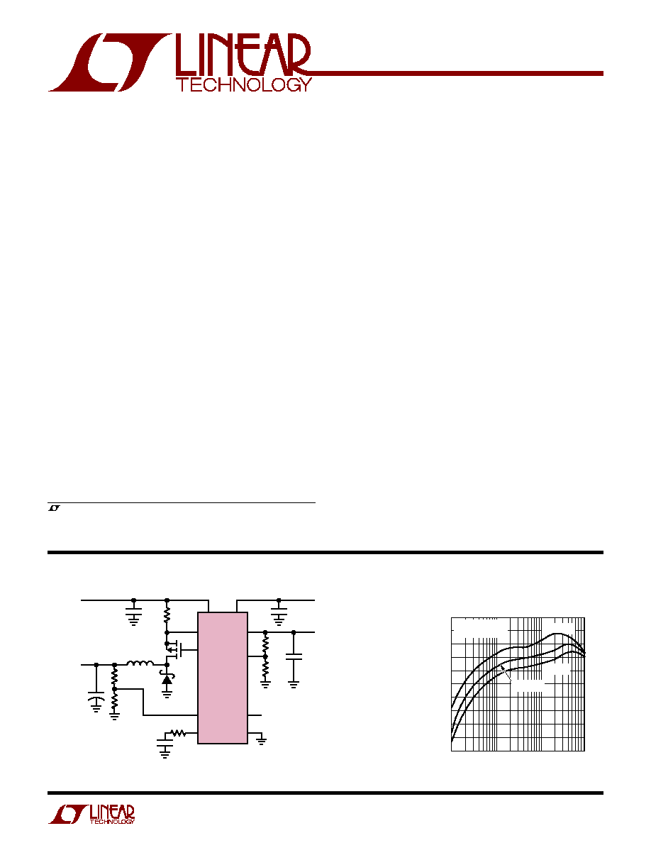
+
SENSE
LTC3700
PGATE
V
FB
LDO
V
FB2
PGOOD
V
IN
V
IN2
I
TH
/RUN
GND
M1
L1
10
µ
H
C2
47
µ
F
6V
100k
80.6k
D1
10k
169k
C4
2.2
µ
F
16V
78.7k
V
OUT2
2.5V AT
150mA
3700 F01
V
IN2
3.3V
V
OUT1
1.8V
AT 1A
C1, C3: TAIYO YUDEN EMK325BJ106MNT
C2: SANYO POSCAP 6TPA47M
C4: MURATA GRM42-6X7R225K016AL
D1: MOTOROLA MBRM120T3
L1: COILTRONICS UP1B-100
M1: Si3443DV
R1: DALE 0.25W
V
IN1
5V
C3
10
µ
F
10V
C1
10
µ
F
10V
R1
0.068
220pF
Figure 1. High Efficiency 5V to 1.8V/1A Buck with 3.3V to 2.5V/150mA LDO
Buck Efficiency vs Load Current
DESCRIPTIO
U
FEATURES
APPLICATIO S
U
TYPICAL APPLICATIO
U
2
LTC3700
3700f
ABSOLUTE
M
AXI
M
U
M
RATINGS
W
W
W
U
(Note 1)
Buck Input Supply Voltage (V
IN
) ................ 0.3V to 10V
SENSE
, PGATE Voltages ............. 0.3V to (V
IN
+ 0.3V)
V
FB
, I
TH
/RUN Voltages .............................. 0.3V to 2.4V
PGATE Peak Output Current (< 10
µ
s) ....................... 1A
LDO Input Supply Voltage (V
IN2
) ................. 0.3V to 6V
LDO, V
FB2
Voltages ..................... 0.3V to (V
IN2
+ 0.3V)
PGOOD Voltage ......................................... 0.3V to 10V
LDO Peak Output Current (< 10
µ
s) ..................... 500mA
Storage Ambient Temperature Range ... 65
°
C to 150
°
C
Operating Temperature Range (Note 2) ... 40
°
C to 85
°
C
Junction Temperature (Note 3) ............................. 150
°
C
Lead Temperature (Soldering, 10 sec).................. 300
°
C
PACKAGE/ORDER I
N
FOR
M
ATIO
N
W
U
U
T
JMAX
= 150
°
C,
JA
= 230
°
C/ W
MS PART MARKING
ORDER PART
NUMBER
LTC3700EMS
LTXN
Consult LTC Marketing for parts specified with wider operating temperature ranges.
ELECTRICAL CHARACTERISTICS
The
q
denotes specifications that apply over the full operating temperature
range, otherwise specifications are at T
A
= 25
°
C. V
IN
= V
IN2
= 4.2V unless otherwise specified. (Note 2)
1
2
3
4
5
V
IN2
LDO
V
FB2
PGOOD
GND
10
9
8
7
6
I
TH
/RUN
V
FB
SENSE
V
IN
PGATE
TOP VIEW
MS PACKAGE
10-LEAD PLASTIC MSOP
PARAMETER
CONDITIONS
MIN
TYP
MAX
UNITS
Buck DC/DC Controller
Input DC Supply Current
Typicals at V
IN
= 4.2V (Note 4)
Normal Operation
2.65V
V
IN
9.8V
210
340
µ
A
Sleep Mode
2.65V
V
IN
9.8V
200
330
µ
A
Shutdown
2.65V
V
IN
9.8V, V
ITH
/RUN = 0V
10
30
µ
A
UVLO
V
IN
< UVLO Threshold
10
30
µ
A
Undervoltage Lockout Threshold
V
IN
Falling
q
1.90
2.10
2.60
V
V
IN
Rising
q
2.00
2.20
2.65
V
Shutdown Threshold (at I
TH
/RUN)
q
0.15
0.30
0.45
V
Start-Up Current Source
V
ITH
/RUN = 0V
0.25
0.5
0.85
µ
A
Regulated Feedback Voltage
(Note 5), 0
°
C to 70
°
C
q
0.780
0.800
0.820
V
(Note 5), 40
°
C to 85
°
C
q
0.770
0.800
0.830
V
Output Voltage Line Regulation
2.65V
V
IN
9.8V (Note 5)
0.1
mV/V
Output Voltage Load Regulation
I
TH
/RUN Sinking 5
µ
A (Note 5)
4
mV/
µ
A
I
TH
/RUN Sourcing 5
µ
A (Note 5)
4
mV/
µ
A
V
FB
Input Current
(Note 5)
10
50
nA
Overvoltage Protect Threshold
Measured at V
FB
0.820
0.860
0.910
V
Overvoltage Protect Hysteresis
20
mV
Oscillator Frequency
V
FB
= 0.8V
500
550
650
kHz
V
FB
= 0V
110
kHz
Gate Drive Rise Time
C
LOAD
= 3000pF
40
ns
Gate Drive Fall Time
C
LOAD
= 3000pF
40
ns
Peak Current Sense Voltage
(Note 6)
120
mV
Peak Current Sense Voltage in Burst Mode
30
mV

3
LTC3700
3700f
Note 1: Absolute Maximum Ratings are those values beyond which the life
of a device may be impaired.
Note 2: The LTC3700 is guaranteed to meet specifications from 0
°
C to
70
°
C. Specifications over the 40
°
C to 85
°
C operating temperature range
are assured by design, characterization and correlation with statistical
process controls.
Note 3: T
J
is calculated from the ambient temperature T
A
and power
dissipation P
D
according to the following formula:
T
J
= T
A
+ (P
D
·
JA
°
C/W)
Note 4: Dynamic supply current is higher due to the gate charge being
delivered at the switching frequency.
Note 5: The LTC3700 is tested in a feedback loop that servos V
FB
to the
output of the error amplifier.
Note 6: Peak current sense voltage is reduced dependent on duty cycle to
a percentage of value as given in Figure 2.
Note 7: Guaranteed by design; not tested in production.
Note 8: PGOOD values are expressed as a percentage difference from the
respective "Regulated Feedback Voltage" as given in the table.
PARAMETER
CONDITIONS
MIN
TYP
MAX
UNITS
ELECTRICAL CHARACTERISTICS
The
q
denotes specifications that apply over the full operating temperature
range, otherwise specifications are at T
A
= 25
°
C. V
IN
= V
IN2
= 4.2V unless otherwise specified. (Note 2)
LDO Regulator
V
IN2
Input Voltage
2.4
6
V
Input DC Supply Current
Typicals at V
IN2
= 4.2V
Normal Operation with Buck Enabled
2.4V
V
IN2
6V
50
100
µ
A
Normal Operation with Buck Undervoltage
2.4V
V
IN2
6V
100
150
µ
A
Shutdown with Buck Enabled
2.4V
V
IN2
6V, V
ITH/RUN
= 0V
0
1
µ
A
Shutdown with Buck Undervoltage
2.4V
V
IN2
6V, V
ITH/RUN
= 0V
8
24
µ
A
Regulated Feedback Voltage
0
°
C
T
A
70
°
C, I
LDO
= 1mA
q
0.780
0.800
0.830
V
40
°
C
T
A
85
°
C, I
LDO
= 1mA
q
0.765
0.800
0.835
V
Output Voltage Line Regulation
(Unity-Gain Feedback)
With Buck Enabled
2.65V
V
IN
9.8V
0.05
mV/V
With Buck Enabled
2.4V
V
IN2
6V, I
LDO
= 1mA
4
mV/V
With Buck Undervoltage
2.4V
V
IN2
6V, I
LDO
= 1mA
4
mV/V
Output Voltage Load Regulation
1mA
I
LOAD
150mA
0.06
0.12
mV/mA
V
FB2
Input Current
0
10
nA
LDO Short-Circuit Current
V
LDO
= 0V
150
200
mA
LDO Dropout
V
IN2
= 3.3V, I
LDO
= 150mA
270
mV
V
IN2
= 6V, I
LDO
= 150mA
170
mV
Overtemperature Trip Point
(Note 7)
150
°
C
Overtemperature Hysteresis
(Note 7)
5
°
C
PGOOD
Feedback Voltage PGOOD Threshold
(Note 8)
PGOOD High-to-Low
V
FB
or V
FB2
Falling
12
7.5
%
V
FB
or V
FB2
Rising
7.5
12
%
PGOOD Low-to-High
V
FB
or V
FB2
Rising
10
5.0
%
V
FB
or V
FB2
Falling
5.0
10
%
PGOOD On-Resistance
V
ITH/RUN
= 0V, V
IN
= V
IN2
= 4.2V, V
PGOOD
= 100mV
135
180
4
LTC3700
3700f
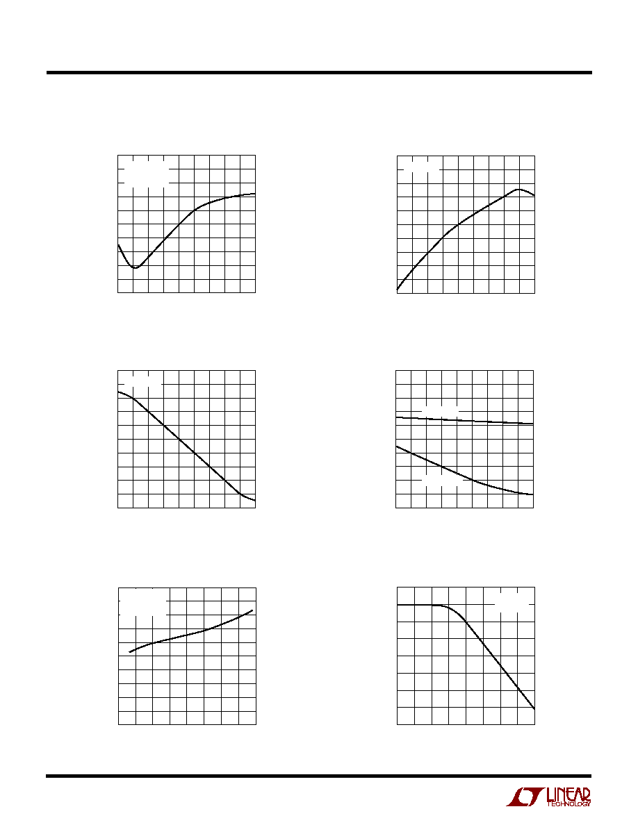
TYPICAL PERFOR A CE CHARACTERISTICS
U
W
BUCK DC/DC CONTROLLER
TEMPERATURE (
°
C)
55 35 15
5
25
45
65
85 105 125
V
FB
VOLTAGE (mV)
3700 G01
805
804
803
802
801
800
799
798
797
796
795
V
IN
= 4.2V
I
TH
/RUN = V
FB
NO LOAD
TEMPERATURE (
°
C)
55 35 15
5
25
45
65
85 105 125
NORMALIZED FREQUENCY SHIFT (%)
3700 G02
10
8
6
4
2
0
2
4
6
8
10
V
IN
= 4.2V
TEMPERATURE (
°
C)
55 35 15
5
25
45
65
85 105 125
TRIP VOLTAGE (V)
3700 G03
2.30
2.28
2.26
2.24
2.20
2.00
2.18
2.16
2.14
2.12
2.10
V
IN
RISING
V
IN
FALLING
TEMPERATURE (
°
C)
55 35 15
5
25
45
65
85 105 125
I
TH
/RUN VOLTAGE (mV)
3700 G04
400
380
360
340
320
300
280
260
240
220
200
V
IN
= 4.2V
DUTY CYCLE (%)
20
30
40
50
60
70
80
90
100
TRIP VOLTAGE (mV)
3700 G05
130
120
110
100
90
80
70
60
50
V
IN
= 4.2V
T
A
= 25
°
C
V
FB
Voltage vs Temperature
Normalized Oscillator Frequency
vs Temperature
Undervoltage Lockout Trip
Voltage vs Temperature
Shutdown Threshold vs
Temperature
Maximum (V
IN
SENSE
) Voltage
vs Duty Cycle
Buck Supply Current
vs Input Voltage
V
IN
INPUT VOLTAGE (V)
2
150
V
IN
SUPPLY CURRENT (
µ
A)
160
180
190
200
250
220
4
6
7
3700 G10
170
230
240
210
3
5
8
9
10
I
TH
/RUN = V
FB
V
IN2
= 0V
T
A
= 25
°
C
5
LTC3700
3700f
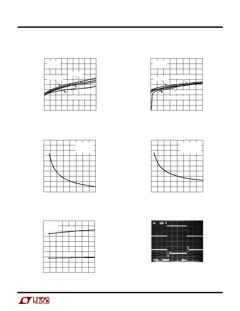
TYPICAL PERFOR A CE CHARACTERISTICS
U
W
V
IN
INPUT VOLTAGE (V)
2
3
4
5
6
7
8
9
10
PGOOD R
ON
(
)
3700 G09
300
270
240
210
180
150
120
90
60
30
0
V
IN2
= 0V
V
PGOOD
= 100mV
T
A
= 25
°
C
PGOOD R
ON
vs Input Voltage
LDO Pass FET R
ON
vs Input
Voltage
V
IN2
INPUT VOLTAGE (V)
2
2.5
3
3.5
4
4.5
5
5.5
6
R
ON
(
)
3700 G08
4.0
3.7
3.4
3.1
2.8
2.5
2.2
1.9
1.6
1.3
1.0
V
IN
= 0
ILDO = 100mA
T
A
= 25
°
C
TEMPERATURE (
°
C)
55 35 15
5
25
45
65
85 105 125
V
FB2
VOLTAGE (mV)
3700 G06
850
840
830
820
810
800
790
780
770
760
750
V
IN2
= 4.2V
LDO = V
FB2
I
LOAD
= 100mA
I
LOAD
= 10mA
I
LOAD
= 10
µ
A
I
LOAD
= 1mA
V
IN2
INPUT VOLTAGE (V)
2.4 2.85 3.3 3.75 4.2 4.65 5.1 5.55
6
V
FB2
VOLTAGE (mV)
3700 G07
850
840
830
820
810
800
790
780
770
760
750
T
A
= 25
°
C
LDO = V
FB2
I
LOAD
= 100mA
I
LOAD
= 1mA
I
LOAD
= 10
µ
A
I
LOAD
= 10mA
V
FB2
Voltage vs Temperature
LDO Line Regulation (V
FB2
Voltage vs Supply)
LDO REGULATOR
Load Transient Response
LDO Supply Current
vs Input Voltage
V
IN2
INPUT VOLTAGE (V)
2
20
V
IN2
SUPPLY CURRENT (
µ
A)
30
50
60
70
120
90
3
4
4.5
3700 G11
40
100
110
80
2.5
3.5
5
5.5
6
V
IN
= 0V
V
IN
= 9.8V
LDO = V
FB2
I
LDO
= 10
µ
A
T
A
= 25
°
C
150
100
50
0
0
I
LDO
(mA)
50mA/DIV
V
LDO
20mV/DIV
AC COUPLED
T
A
= 25
°
C
20
µ
s/DIV
3700 G12
V
IN2
= 3.3V
V
LDO
= 2.5V
C
LDO
= 10
µ
F