 | ÐлекÑÑоннÑй компоненÑ: LTC3714EG | СкаÑаÑÑ:  PDF PDF  ZIP ZIP |
Äîêóìåíòàöèÿ è îïèñàíèÿ www.docs.chipfind.ru
LTC3714
1
3714f
Intel Compatible,
Wide Operating Range, Step-Down Controller
with Internal Op Amp
s
True Current Mode with Ultrafast Transient
Response
s
Stable with Ceramic C
OUT
s
t
ON(MIN)
< 100ns for Operation from High Input
Ranges
s
Supports Active Voltage Positioning
s
No Sense Resistor Required
s
5-Bit VID Programmable Output Voltage: 0.6V to 1.75V
s
Dual N-Channel MOSFET Synchronous Drive
s
Programmable Output Offsets
s
Power Good Output Voltage Monitor
s
Wide V
IN
Range: 4V to 36V
s
±
1% 0.6V Reference
s
Adjustable Frequency
s
Programmable Soft-Start
s
Output Overvoltage Protection
s
Optional Short-Circuit Shutdown Timer
s
Forced Continuous Control Pin
s
Logic Controlled Micropower Shutdown: I
Q
30
µ
A
s
Available in 0.209" Wide 28-Lead SSOP Package
s
Power Supply for Mobile Pentium
®
Processors and
Transmeta Processors
s
Notebook and Portable Computers
, LTC and LT are registered trademarks of Linear Technology Corporation.
Pentium is a registered trademark of Intel Corporation.
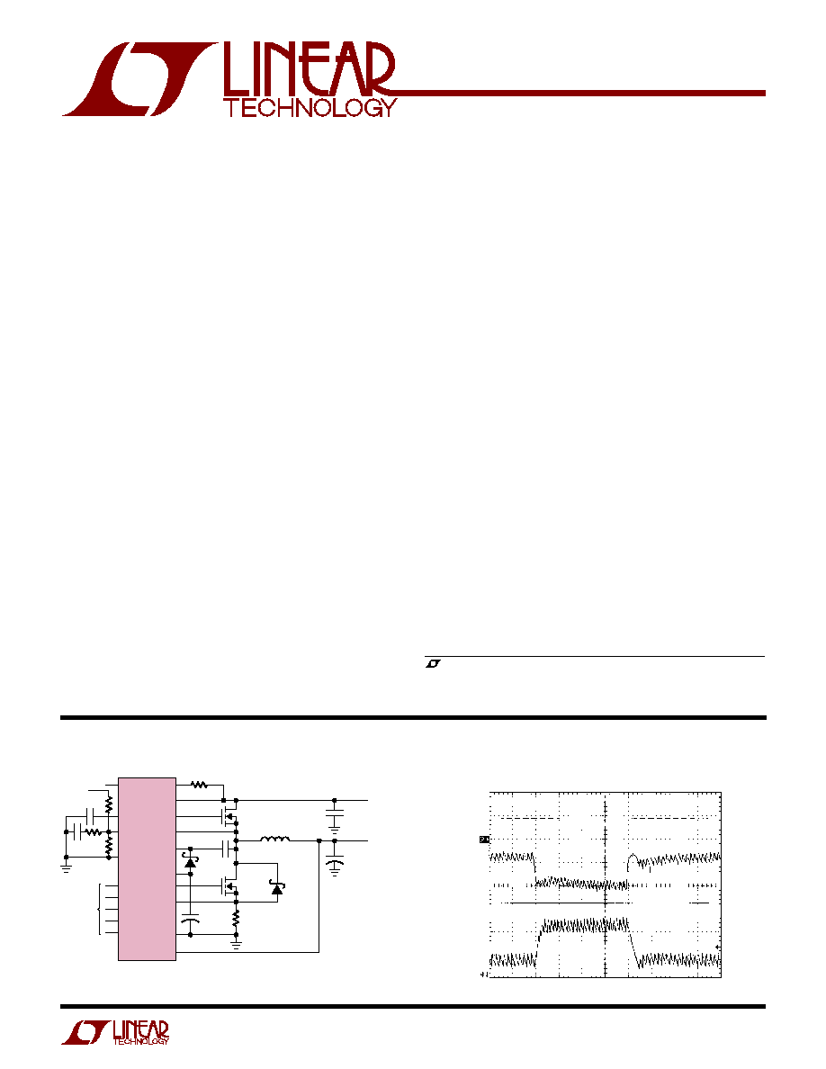
Figure 1. High Efficiency Step-Down Converter
Transient Response of 8A to 23A Output Load Step
The LTC
®
3714 is a synchronous step-down switching
regulator controller for CPU power. An output voltage
between 0.6V and 1.75V is selected by a 5-bit code (Intel
mobile VID specification). The controller uses a constant
on-time, valley current control architecture to deliver very
low duty cycles without requiring a sense resistor. Oper-
ating frequency is selected by an external resistor and is
compensated for variations in V
IN
and V
OUT
.
Discontinuous mode operation provides high efficiency
operation at light loads. A forced continuous control pin
reduces noise and RF interference and can assist second-
ary winding regulation by disabling discontinuous mode
when the main output is lightly loaded. Internal op amp
allows programmable offsets to the output voltage during
power saving modes.
Fault protection is provided by internal foldback current
limiting, an output overvoltage comparator and optional
short-circuit shutdown timer. Soft-start capability for sup-
ply sequencing is accomplished using an external timing
capacitor. The regulator current limit level is user pro-
grammable. Wide supply range allows operation from 4V
to 36V at the input.
+
D
B
CMDSH-3
D1*
UPS840
*OPTIONAL
L1
0.68
µ
H
C
VCC
4.7
µ
F
10
µ
F
35V
×
4
V
IN
5V TO 24V
V
OUT
0.6V TO 1.75V
23A
+
C
OUT
270
µ
F
2V
×
4
M2
IRF7811
×
3
0.003
*
3714 F01
M1
IRF7811
×
2
R
ON
C
SS
0.1
µ
F
INTV
CC
I
ON
V
IN
TG
SW
BOOST
RUN/SS
I
TH
SGND
INTV
CC
BG
PGND
SENSE
5-BIT
VID
V
OSENSE
PGOOD
VID0
VID1
VID2
VID3
VID4
C
B
, 0.22
µ
F
R
C
LTC3714
C
C
APPLICATIO S
U
FEATURES
TYPICAL APPLICATIO
U
DESCRIPTIO
U
1.395V
V
OUT
(1.35V)
50mV/DIV
1.213V
23A
8A
I
LOAD
10A/DIV
20
µ
s/DIV
3714 TA03
LTC3714
2
3714f
(Note 1)
Input Supply Voltage (V
IN
), I
ON
..................36V to 0.3V
Boosted Topside Driver Supply Voltage
(BOOST) ................................................... 42V to 0.3V
SW, SENSE Voltages ................................... 36V to 5V
EXTV
CC
, (BOOST SW), RUN/SS, VID0-VID4,
PGOOD, FCB Voltages ............................... 7V to 0.3V
V
ON
, V
RNG
Voltages ................(INTV
CC
+ 0.3V) to 0.3V
I
TH
, V
FB
, V
OSENSE
Voltages ....................... 2.7V to 0.3V
TG, BG, INTV
CC
, EXTV
CC
Peak Currents .................... 2A
TG, BG, INTV
CC
, EXTV
CC
RMS Currents .............. 50mA
OPV
IN
, OP
+
, OP
.......................................................
0V to 18V
Operating Ambient Temperature Range
LTC3714EG (Note 2) .......................... 40
°
C to 85
°
C
Junction Temperature (Note 3) ............................ 125
°
C
Storage Temperature Range ................. 65
°
C to 150
°
C
Lead Temperature (Soldering, 10 sec).................. 300
°
C
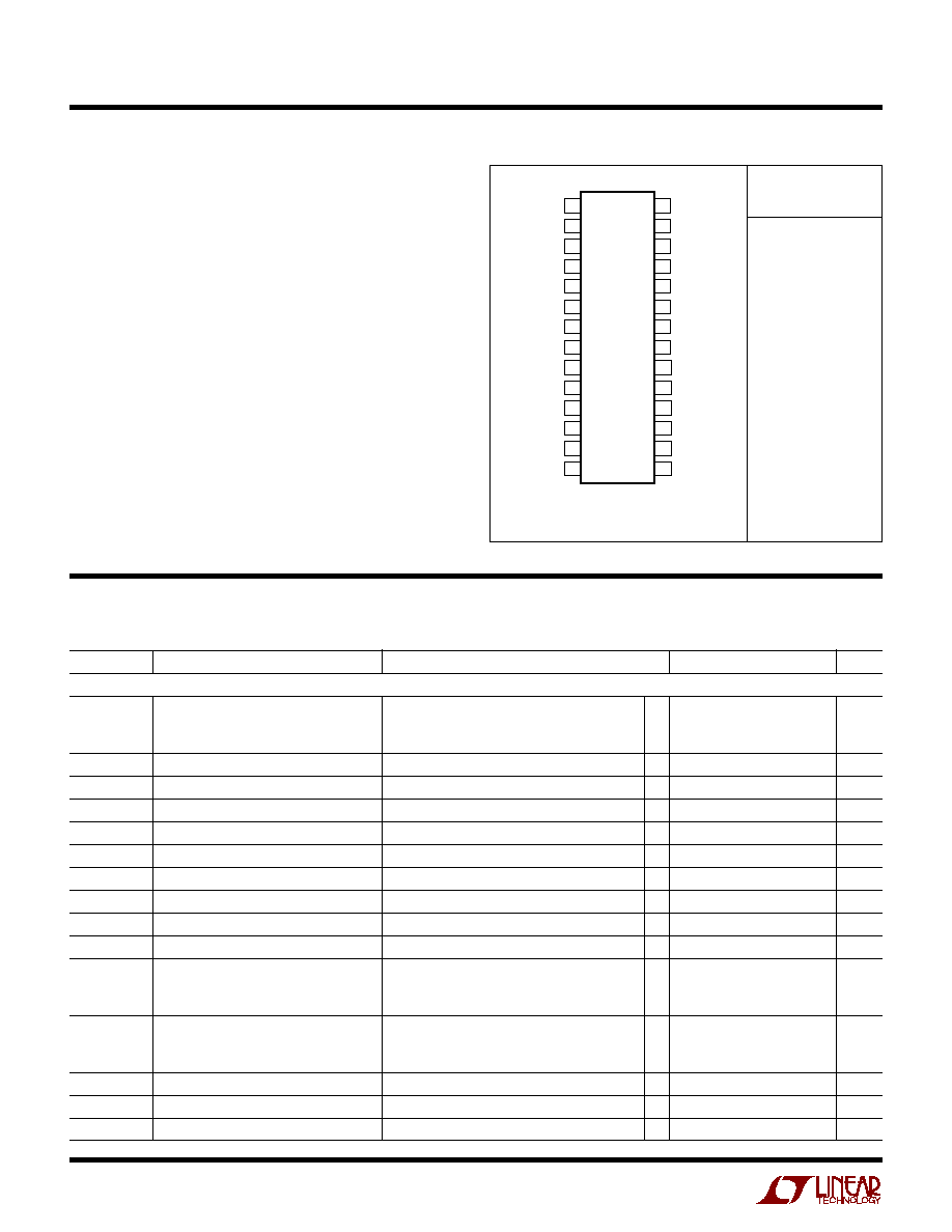
ORDER PART
NUMBER
LTC3714EG
T
JMAX
= 125
°
C,
JA
= 130
°
C/ W
ABSOLUTE AXI U RATI GS
W
W
W
U
PACKAGE/ORDER I FOR ATIO
U
U
W
1
2
3
4
5
6
7
8
9
10
11
12
13
14
TOP VIEW
G PACKAGE
28-LEAD PLASTIC SSOP
28
27
26
25
24
23
22
21
20
19
18
17
16
15
BG
PGND
SENSE
SW
TG
BOOST
VID0
VID1
VID2
RUN/SS
V
ON
PGOOD
V
RNG
I
TH
INTV
CC
V
IN
EXTV
CC
VID4
VID3
V
OSENSE
VFB
I
ON
FCB
SGND
OPOUT
OP
+
OP
OPV
IN
The
q
denotes specifications which apply over the full operating
temperature range, otherwise specifications are T
A
= 25
°
C. V
IN
= 15V unless otherwise noted.
ELECTRICAL CHARACTERISTICS
SYMBOL
PARAMETER
CONDITIONS
MIN
TYP
MAX
UNITS
Main Control Loop
I
Q
Input DC Supply Current
Normal
900
2000
µ
A
Shutdown Supply Current
15
30
µ
A
V
FB
Feedback Reference Voltage
I
TH
= 1.2V (Note 4)
q
0.594
0.600
0.606
V
V
FB(LINEREG)
Feedback Voltage Line Regulation
V
IN
= 4V to 30V (Note 4), I
TH
= 1.2V
0.002
%/V
V
FB(LOADREG)
Feedback Voltage Load Regulation
I
TH
= 0.5V to 1.9V (Note 4)
q
0.05
0.3
%
g
m(EA)
Error Amplifier Transconductance
I
TH
= 1.2V (Note 4)
q
1.4
1.7
2
ms
V
FCB
Forced Continuous Threshold
q
0.57
0.6
0.63
V
I
FCB
Forced Continuous Current
V
FCB
= 0.6V
1
2
µ
A
t
ON
On-Time
I
ON
= 60
µ
A, V
ON
= 1.5V
200
250
300
ns
t
ON(MIN)
Minimum On-Time
I
ON
= 180
µ
A, V
ON
= 0V
50
100
ns
t
OFF(MIN)
Minimum Off-Time
I
ON
= 60
µ
A, V
ON
= 1.5V
250
400
ns
V
SENSE(MAX)
Maximum Current Sense Threshold
V
RNG
= 1V, V
FB
= 0.56V
q
113
133
153
mV
V
RNG
= 0V, V
FB
= 0.56V
q
79
93
107
mV
V
RNG
= INTV
CC
, V
FB
= 0.56V
q
158
186
214
mV
V
SENSE(MIN)
Minimum Current Sense Threshold
V
RNG
= 1V, V
FB
= 0.64V
67
mV
V
RNG
= 0V, V
FB
= 0.64V
33
mV
V
RNG
= INTV
CC
, V
FB
= 0.64V
93
mV
V
FB(OV)
Output Overvoltage Fault Threshold
7.5
10
12.5
%
V
FB(UV)
Output Undervoltage Fault Threshold
340
400
460
mV
V
RUN/SS(ON)
RUN Pin Start Threshold
q
0.8
1.5
2
V
Consult LTC Marketing for parts specified with wider operating temperature ranges.
LTC3714
3
3714f
The
q
denotes specifications which apply over the full operating
temperature range, otherwise specifications are T
A
= 25
°
C. V
IN
= 15V unless otherwise noted.
ELECTRICAL CHARACTERISTICS
SYMBOL
PARAMETER
CONDITIONS
MIN
TYP
MAX
UNITS
V
IN
= 5V unless otherwise noted.
V
RUN/SS(LE)
RUN Pin Latchoff Enable Threshold
RUN/SS Pin Rising
4
4.5
V
V
RUN/SS(LT)
RUN Pin Latchoff Threshold
RUN/SS Pin Falling
3.5
4.2
V
I
RUN/SS(C)
Soft-Start Charge Current
0.5
1.2
3
µ
A
I
RUN/SS(D)
Soft-Start Discharge Current
0.8
1.8
3
µ
A
V
IN(UVLO)
Undervoltage Lockout Threshold
V
IN
Falling
q
3.4
3.9
V
V
IN(UVLOR)
Undervoltage Lockout Threshold
V
IN
Rising
q
3.5
4
V
TG R
UP
TG Driver Pull-Up On Resistance
TG High
2
3
TG R
DOWN
TG Driver Pull-Down On Resistance
TG Low
2
3
BG R
UP
BG Driver Pull-Up On Resistance
BG High
3
4
BG R
DOWN
BG Driver Pull-Down On Resistance
BG Low
1
2
TG t
r
TG Rise Time
C
LOAD
= 3300pF
20
ns
TG t
f
TG Fall Time
C
LOAD
= 3300pF
20
ns
BG t
r
BG Rise Time
C
LOAD
= 3300pF
20
ns
BG t
f
BG Fall Time
C
LOAD
= 3300pF
20
ns
Internal V
CC
Regulator
V
INTVCC
Internal V
CC
Voltage
6V < V
IN
< 30V, V
EXTVCC
= 4V
q
4.7
5
5.3
V
V
LDO(LOADREG)
Internal V
CC
Load Regulation
I
CC
= 0mA to 20mA, V
EXTVCC
= 4V
0.1
±
2
%
V
EXTVCC
EXTV
CC
Switchover Voltage
I
CC
= 20mA, V
EXTVCC
Rising
q
4.5
4.7
V
V
EXTVCC
EXTV
CC
Switch Drop Voltage
I
CC
= 20mA, V
EXTVCC
= 5V
150
300
mV
V
EXTVCC(HYS)
EXTV
CC
Switchover Hysteresis
200
mV
PGOOD Output
V
FBH
PGOOD Upper Threshold
V
FB
Rising
7.5
10
12.5
%
V
FBL
PGOOD Lower Threshold
V
FB
Falling
7.5
10
12.5
%
V
FB(HYS)
PGOOD Hysteresis
V
FB
Returning
1
2.5
%
V
PGL
PGOOD Low Voltage
I
PGOOD
= 1mA
0.15
0.4
V
VID DAC
V
VID(T)
VID0-VID4 Logic Threshold Voltage
0.4
1.2
2
V
I
VID(PULLUP)
VID0-VID4 Pull-Up Current
V
VID0
to V
VID4
= 0V
2.5
µ
A
V
VID(PULLUP)
VID0-VID4 Pull-Up Voltage
V
VID0
to V
VID4
Open
4.5
V
I
VID(LEAK)
VID0-VID4 Leakage Current
V
VID0
to V
VID4
= 5V, V
RUN/SS
= 0V
0.01
1
µ
A
R
VID
Resistance from V
OSENSE
to V
FB
6
10
14
K
V
OSENSE
DAC Output Accuracy
V
OSENSE
Programmed from
0.45
0
0.25
%
0.6V to 1.75V (Note 5)
Internal Op Amp
V
OS
Input Offset Voltage
400
1000
µ
V
I
OS
Input Offset Current
4
10
nA
I
B
Input Bias Current
45
80
nA
CMRR
Common Mode Rejection Ratio
V
CM
= 0V to (V
CC
1V)
100
dB
V
CM
= 0V to 18V
80
dB
LTC3714
4
3714f
The
q
denotes specifications which apply over the full operating
temperature range, otherwise specifications are T
A
= 25
°
C. V
IN
= 5V unless otherwise noted.
Note 1: Absolute Maximum Ratings are those values beyond which the life
of a device may be impaired.
Note 2: The LTC3714E is guaranteed to meet performance specifications
from 0
°
C to 70
°
C. Specifications over the 40
°
C to 85
°
C operating
temperature range are assured by design, characterization and correlation
with statistical process controls.
Note 3: T
J
is calculated from the ambient temperature T
A
and power
dissipation P
D
as follows:
LTC3714EG: T
J
= T
A
+ (P
D
· 130
°
C/W)
Note 4: The LTC3714 is tested in a feedback loop that adjusts V
FB
to
achieve a specified error amplifier output voltage (I
TH
).
Note 5: The LTC3714 VID DAC is tested in a feedback loop that adjusts
V
OSENSE
to achieve a specified feedback voltage (V
FB
= 0.6V) for each DAC
VID code.
ELECTRICAL CHARACTERISTICS
SYMBOL
PARAMETER
CONDITIONS
MIN
TYP
MAX
UNITS
PSRR
Power Supply Rejection Ratio
OPV
IN
= 3V to 12.5V, OP
OUT
= V
O
= 1V
100
dB
A
VOL
Large-Signal Voltage Gain
OPV
IN
= 5V, OP
OUT
= 500mV to 4.5V, R
L
= 10k
1500
V/mV
V
OL
Output Voltage Swing LOW
OPV
IN
= 5V, I
SINK
= 5mA
q
165
500
mV
V
OH
Output Voltage Swing HIGH
OPV
IN
= 5V, I
SOURCE
= 5mA
q
4.5
4.87
V
I
SC
Short-Circuit Current
Short to GND
30
mA
Short to OPV
IN
40
mA
I
S
Supply Current
170
300
µ
A
LTC3714
5
3714f
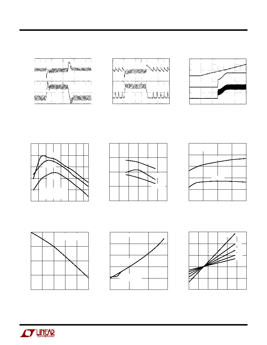
TYPICAL PERFOR A CE CHARACTERISTICS
U
W
Efficiency vs Load Current
Efficiency vs Input Voltage
Frequency vs Input Voltage
INPUT VOLTAGE (V)
5
FREQUENCY (kHz)
240
260
25
3714 G05
220
200
10
15
20
300
280
I
OUT
= 10A
FCB = 0V
FIGURE 1 CIRCUIT
I
OUT
= 0A
Load Regulation
LOAD CURRENT (A)
0
V
OUT
(%)
0.2
0.1
8
3714 G06
0.3
0.4
2
4
6
10
0
NO AVP
FIGURE 1 CIRCUIT
I
TH
Voltage vs Load Current
LOAD CURRENT (A)
0
I
TH
VOLTAGE (V)
1.0
1.5
3714 G07
0.5
0
5
10
15
2.5
2.0
CONTINUOUS
MODE
DISCONTINUOUS
MODE
FIGURE 1 CIRCUIT
Current Sense Threshold
vs I
TH
Voltage
I
TH
VOLTAGE (V)
0
200
CURRENT SENSE THRESHOLD (mV)
100
0
100
200
300
0.5
1.0
1.5
2.0
3714 G08
2.5
3.0
V
RNG
=
1V
0.7V
0.5V
1.4V
2V
Transient Response
(Discontinuous Mode)
Transient Response
V
OUT
50mV/DIV
I
L
5A/DIV
20
µ
s/DIV
3714 G01
LOAD STEP 0A TO 10A
V
IN
= 15V
V
OUT
= 1.5V
FCB = 0V
FIGURE 1 CIRCUIT
V
OUT
50mV/DIV
I
L
5A/DIV
20
µ
s/DIV
3714 G02
LOAD STEP 1A TO 10A
V
IN
= 15V
V
OUT
= 1.5V
FCB = INTV
CC
FIGURE 1 CIRCUIT
Start-Up
RUN/SS
2V/DIV
I
L
5A/DIV
50ms/DIV
3714 G19
V
IN
= 15V
V
OUT
= 1.25V
R
LOAD
= 0.125
V
OUT
500mV/DIV
LOAD CURRENT (A)
0
EFFICIENCY (%)
3714 G03
3
6
9
12
15
18
21
95
90
85
80
75
70
V
IN
= 8.5V
V
OUT
= 1.35V
FREQUENCY = 300kHz
FIGURE 1 CIRCUIT
V
IN
= 15V
V
IN
= 24V
INPUT VOLTAGE (V)
0
EFFICIENCY (%)
100
90
80
70
60
5
10
15
20
3714 G04
25
30
I
OUT
= 10A
I
OUT
= 1A
I
OUT
= 23A