 | ÐлекÑÑоннÑй компоненÑ: LTC3723-1 | СкаÑаÑÑ:  PDF PDF  ZIP ZIP |
372312i Layout
LTC3723-1/LTC3723-2
1
372312i
Information furnished by Linear Technology Corporation is believed to be accurate and reliable.
However, no responsibility is assumed for its use. Linear Technology Corporation makes no represen-
tation that the interconnection of its circuits as described herein will not infringe on existing patent rights.
The LTC
®
3723-1/LTC3723-2 synchronous push-pull PWM
controllers provide all of the control and protection func-
tions necessary for compact and highly efficient, isolated
power converters. High integration minimizes external
component count, while preserving design flexibility.
The robust push-pull output stages switch at half the
oscillator frequency. Dead-time is independently pro-
grammed with an external resistor. Synchronous rectifier
timing is adjustable to optimize efficiency. A UVLO pro-
gram input provides precise system turn-on and turn off
voltages. The LTC3723-1 features peak current mode
control with programmable slope compensation and lead-
ing edge blanking, while the LTC3723-2 employs voltage
mode control with voltage feedforward capability.
The LTC3723-1/LTC3723-2 feature extremely low operat-
ing and start-up currents. Both devices provide reliable
short-circuit and overtemperature protection. The
LTC3723-1/LTC3723-2 are offered in a 16-pin SSOP
package.
s
Telecommunications, Infrastructure Power Systems
s
Distributed Power Architectures
, LTC and LT are registered trademarks of Linear Technology Corporation.
s
High Efficiency Synchronous Push-Pull PWM
s
1.5A Sink, 1A Source Output Drivers
s
Adjustable Push-Pull Dead-Time and Synchronous
Timing
s
Adjustable System Undervoltage Lockout and
Hysteresis
s
Adjustable Leading Edge Blanking
s
Low Start-Up and Quiescent Currents
s
Current Mode (LTC3723-1) and Voltage Mode
(LTC3723-2) Operation
s
Single Resistor Slope Compensation
s
V
CC
UVLO and 25mA Shunt Regulator
s
Programmable Fixed Frequency Operation to 1MHz
s
50mA Synchronous Output Drivers
s
Soft-Start, Cycle-by-Cycle Current Limiting and
Hiccup Mode Short-Circuit Protection
s
5V, 15mA Low Dropout Regulator
s
Available in 16-Pin SSOP Package
APPLICATIO S
U
FEATURES
DESCRIPTIO
U
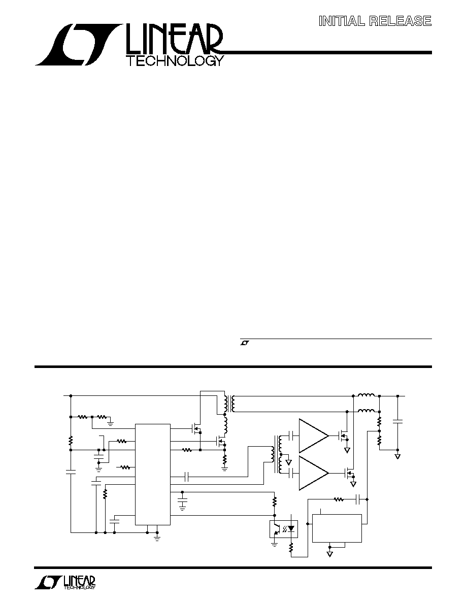
TYPICAL APPLICATIO
U
Synchronous Push-Pull
PWM Controllers
October 2003
Final Electrical Specifications
1
µ
F
1/2
LTC1693
1/2
LTC1693
IRL3103
0.05
IRL3103
1
µ
F
1
µ
F
IRF1310N
IRF1310N
·
·
·
330
2
µ
H
2
µ
H
25k
8k
470
µ
F
V
OUT
12V/15A
1
µ
F
DRVA
DRVB
CS
V
CC
DPRG
LTC3723-1
SDRA
SDRB
V
REF
COMP
UVLO
SPRG
C
T
R
LEB
SS
FB
GND
V
OUT
10k
1
µ
F
470
3.3k
V
+
V
OUT
R
TOP
GND-F
LT1431
GND-S
COLL
R
REF
COMP
R
MID
372312 TA01
1
µ
F
330pF
22
µ
F
3.9nF
100k
V
IN
36V TO 72V
20k
20k
30k
FROM
AUXILIARY
WINDING
51k
300k
V
REF
Isolated 36V to 72V DC to 12V/15A Push-Pull Converter
LTC3723-1/LTC3723-2
2
372312i
V
CC
to GND (Low Impedance Source) ....... 0.3V to 10V
(Chip Self-Regulates at 10.3V)
UVLO to GND ............................................. 0.3V to V
CC
All Other Pins to GND
(Low Impedance Source) ......................... 0.3V to 5.5V
V
CC
(Current Fed) ................................................. 40mA
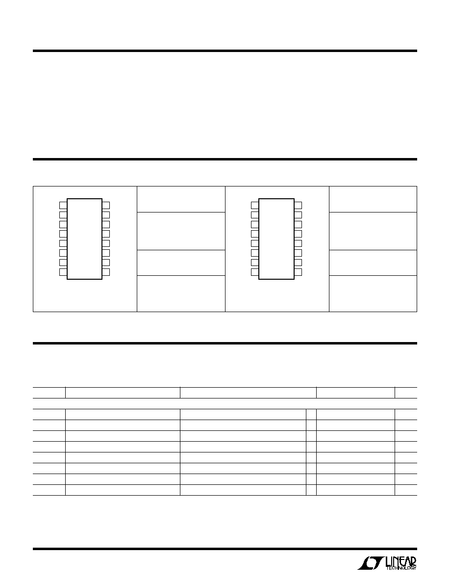
ORDER PART
NUMBER
GN PART
MARKING
T
JMAX
= 125
°
C,
JA
= 100
°
C/W
Consult LTC Marketing for parts specified with wider operating temperature ranges.
37231
LTC3723EGN-1
ABSOLUTE AXI U
RATI GS
W
W
W
U
PACKAGE/ORDER I FOR ATIO
U
U
W
(Note 1)
ELECTRICAL CHARACTERISTICS
The
q
denotes the specifications which apply over the full operating
temperature range, otherwise specifications are at T
A
= 25
°
C. V
CC
= 9.5V unless otherwise noted.
V
REF
Output Current ............................... Self-Regulated
Operating Temperature (Notes 5,6)
LTC3723E ........................................... 40
°
C to 85
°
C
Storage Temperature Range ................. 65
°
C to 125
°
C
Lead Temperature (Soldering, 10sec)................... 300
°
C
ORDER PART
NUMBER
GN PART
MARKING
37232
LTC3723EGN-2
T
JMAX
= 125
°
C,
JA
= 100
°
C/W
1
2
3
4
5
6
7
8
TOP VIEW
GN PACKAGE
16-LEAD PLASTIC SSOP
16
15
14
13
12
11
10
9
V
REF
SDRB
SDRA
DRVB
V
CC
DRVA
GND
C
T
SPRG
UVLO
SS
FB
R
LEB
COMP
CS
DPRG
1
2
3
4
5
6
7
8
TOP VIEW
GN PACKAGE
16-LEAD PLASTIC SSOP
16
15
14
13
12
11
10
9
V
REF
SDRB
SDRA
DRVB
V
CC
DRVA
GND
C
T
SPRG
UVLO
SS
FB
DPRG
COMP
CS
RAMP
SYMBOL
PARAMETER
CONDITIONS
MIN
TYP
MAX
UNITS
Input Supply
V
CCUV
V
CC
Undervoltage Lockout
Measured on V
CC
10.25
10.7
V
V
CCHY
V
CC
UVLO Hysteresis
Measured on V
CC
3.8
4.2
V
I
CCST
Start-Up Current
V
CC
= V
UVLO
0.3V
q
145
230
µ
A
I
CCRN
Operating Current
No Load on Outputs
3
6
mA
V
SHUNT
Shunt Regulator Voltage
Current into V
CC
= 10mA
10.3
10.8
V
R
SHUNT
Shunt Resistance
Current into V
CC
= 10mA to 17mA
1.4
3.5
SUVLO
System UVLO Threshold
Measured on UVLO Pin, 10mA into V
CC
4.8
5.0
5.2
V
SHYST
System UVLO Hysteresis Current
Current Flows Out of UVLO Pin, 10mA into V
CC
8.5
10
11.5
µ
A
LTC3723-1/LTC3723-2
3
372312i
ELECTRICAL CHARACTERISTICS
The
q
denotes the specifications which apply over the full operating
temperature range, otherwise specifications are at T
A
= 25
°
C. V
CC
= 9.5V unless otherwise noted.
SYMBOL
PARAMETER
CONDITIONS
MIN
TYP
MAX
UNITS
Pulse Width Modulator
ROS
Ramp Offset Voltage
Measured on COMP, RAMP = 0V
0.65
V
I
RMP
Ramp Discharge Current
RAMP = 1V, COMP = 0V, C
T
= 4V, 3723-1 Only
50
mA
I
SLP
Slope Compensation Current
Measured on CS, C
T
= 1V, 3723-1 Only
30
µ
A
C
T
= 2.25V
68
µ
A
DCMAX
Maximum Duty Cycle
COMP = 4.5V
q
47
48.2
50
%
DCMIN
Minimum Duty Cycle
COMP = 0V
q
0
%
DTADJ
Dead-Time
130
ns
Oscillator
OSCI
Initial Accuracy
T
A
= 25
°
C, C
T
= 270pF
220
250
280
kHz
OSCT
V
CC
Variation
V
CC
= 6.5V to 9.5V, Overtemperature
q
3
3
%
OSCV
C
T
Ramp Amplitude
Measured on C
T
2.35
V
Error Amplifier
V
FB
FB Input Voltage
COMP = 2.5V, (Note 3)
1.172
1.2
1.22
V
FB
I
FB Input Range
Measured on FB, (Note 4)
0.3
2.5
V
AVOL
Open-Loop Gain
COMP = 1V to 3V, (Note 3)
70
90
dB
I
IB
Input Bias Current
COMP = 2.5V, (Note 3)
5
50
nA
V
OH
Output High
Load on COMP = 100
µ
A
4.7
4.92
V
V
OL
Output Low
Load on COMP = 100
µ
A
0.27
0.5
V
I
SOURCE
Output Source Current
COMP = 2.5V
400
700
µ
A
I
SINK
Output Sink Current
COMP = 2.5V
2
5
mA
Reference
V
REF
Initial Accuracy
T
A
= 25
°
C, Measured on V
REF
4.925
5.00
5.075
V
REFLD
Load Regulation
Load on V
REF
= 100
µ
A to 5mA
2
15
mV
REFLN
Line Regulation
V
CC
= 6.5V to 9.5V
1
10
mV
REFTV
Total Variation
Line, Load and Temperature
q
4.900
5.000
5.100
V
REFSC
Short-Circuit Current
V
REF
Shorted to GND
18
30
45
mA
Push-Pull Outputs
DRVH(x)
Output High Voltage
I
OUT(x)
= 100mA
9
9.2
V
DRVL(x)
Output Low Voltage
I
OUT(x)
= 100mA
0.17
0.25
V
RDH(x)
Pull-Up Resistance
I
OUT(x)
= 10mA to 100mA
2.9
4
RDL(x)
Pull-Down Resistance
I
OUT(x)
= 10mA to 100mA
1.7
2.5
TDR(x)
Rise-Time
C
OUT(x)
= 1nF
10
ns
TDF(x)
Fall-Time
C
OUT(x)
= 1nF
10
ns
LTC3723-1/LTC3723-2
4
372312i
SYMBOL
PARAMETER
CONDITIONS
MIN
TYP
MAX
UNITS
ELECTRICAL CHARACTERISTICS
The
q
denotes the specifications which apply over the full operating
temperature range, otherwise specifications are at T
A
= 25
°
C. V
CC
= 9.5V unless otherwise noted.
Note 1: Absolute Maximum Ratings are those values beyond which the life
of a device may be impaired.
Note 2: Includes leading edge blanking delay, R
LEB
= 20k, not tested in
production.
Note 3: FB is driven by a servo loop amplifier to control V
COMP
for these
tests.
Note 4: Set FB to 0.3V, 2.5V and insure that COMP does not phase invert.
Note 5: The LTC3723E1/LTC3723E-2 are guaranteed to meet
performance specifications from 0
°
C to 85
°
C. Specifications over the
Synchronous Outputs
OUTH(x)
Output High Voltage
I
OUT(x)
= 30mA
9.0
9.2
V
OUTL(x)
Output Low Voltage
I
OUT(x)
= 30mA
0.44
0.6
V
RHI(x)
Pull-Up Resistance
I
OUT(x)
= 10mA to -30mA
11
15
RLO(x)
Pull-Down Resistance
I
OUT(x)
= 10mA to -30mA
15
20
TR(x)
Rise-Time
C
OUT(x)
= 50pF
10
ns
TF(x)
Fall-Time
C
OUT(x)
= 50pF
10
ns
Current Limit and Shutdown
CLPP
Pulse by Pulse Current Limit Threshold
Measured on CS
280
300
320
mV
CLSD
Shutdown Current Limit Threshold
Measured on CS
475
600
725
mV
CLDEL
Current Limit Delay to Output
100mV Overdrive on CS, (Note 2)
80
ns
SSI
Soft-Start Current
SS = 2.5V
10
13
16
µ
A
SSR
Soft-Start Reset Threshold
Measured on SS
0.7
0.4
0.1
V
FLT
Fault Reset Threshold
Measured on SS
4.5
4.2
3.5
V
40
°
C to 85
°
C operating temperature range are assured by design,
characterization and correlation with statistical process controls.
Note 6: This IC includes overtemperature protection that is intended to
protect the device during momentary overload conditions. Junction
temperature will exceed 125
°
C when overtemperature protection is active.
Continuous operation above the specified maximum operating junction
temperature may impair device reliability.
V
REF
(Pin 1/Pin 1): Output of the 5.0V Reference. V
REF
is
capable of supplying up to 18mA to external circuitry. V
REF
should be decoupled to GND with a 1
µ
F ceramic capacitor.
SDRB (Pin 2/Pin 2): 50mA Driver for Synchronous Recti-
fier associated with DRVB.
SDRA (Pin 3/Pin 3): 50mA Driver for Synchronous Recti-
fier associated with DRVA.
DRVB (Pin 4/Pin 4): High Speed 1.5A Sink, 1A Source
Totem Pole MOSFET Driver. Connect to gate of external
push-pull MOSFET with as short a PCB trace as practical
to preserve drive signal integrity. A low value resistor
connected between DRVA and the MOSFET gate is op-
DESCRIPTIO S
U
PI
U
tional and will improve the gate drive signal quality if the
PCB trace from the driver to the MOSFET cannot be made
short.
V
CC
(Pin 5/Pin 5): Supply Voltage Input to the LTC3723-1/
LTC3723-2 and 10.25V Shunt Regulator. The chip is
enabled after V
CC
has risen high enough to allow the V
CC
shunt regulator to conduct current and the UVLO com-
parator threshold is exceeded. Once the V
CC
shunt regu-
lator has turned on, V
CC
can drop to as low as 6V (typical)
and maintain operation. Bypass V
CC
to GND with a high
quality 1
µ
F or larger ceramic capacitor to supply the
transient currents caused by the high speed switching and
capacitive loads presented by the on chip totem pole
drivers.
(LTC3723-1/LTC3723-2)

LTC3723-1/LTC3723-2
5
372312i
DRVA (Pin 6/Pin 6): High Speed 1.5A Sink, 1A Source
Totem Pole MOSFET Driver. Connect to gate of external
push-pull MOSFET with as short a PCB trace as practical
to preserve drive signal integrity. A low value resistor
connected between DRVA and the MOSFET gate is op-
tional and will improve the gate drive signal quality if the
PCB trace from the driver to the MOSFET cannot be made
short.
GND (Pin 7/Pin 7): All circuits in the LTC3723 are refer-
enced to GND. Use of a ground plane is highly recom-
mended. V
IN
and V
REF
bypass capacitors must be termi-
nated with a star configuration as close to GND as practical
for best performance.
C
T
(Pin 8/Pin 8): Timing Capacitor for the Oscillator. Use
a
±
5% or better low ESR ceramic capacitor for best
results. C
T
ramp amplitude is 2.35V peak-to-peak
(typical).
DPRG (Pin 9/Pin 12): Programming Input for Push-Pull
Dead-Time. Connect a resistor between DPRG and V
REF
to
program the dead-time. The dead-time is approximately
equal to (1.30 · 10
12
· RDPRG). The nominal voltage on
DPRG is 2V.
RAMP (N/A/Pin 9): Input to PWM Comparator for
LTC3723-2 Only (Voltage Mode Controller). The voltage
on RAMP is internally level shifted by 650mV.
CS (Pin 10/Pin 10): Input to Pulse-by-Pulse and Overload
Current Limit Comparators, Output of Slope Compensa-
tion Circuitry. The pulse-by-pulse comparator has a nomi-
nal 300mV threshold, while the overload comparator has
a nominal 600mV threshold. An internal switch discharges
CS to GND after every timing period. Slope compensation
current flows out of CS during the PWM period.
An external resistor connected from CS to the external
current sense resistor programs the amount of slope
compensation.
COMP (Pin 11/Pin 11): Error Amplifier Output, Inverting
Input to Phase Modulator.
DESCRIPTIO S
U
PI
U
(LTC3723-1/LTC3723-2)
R
LEB
(Pin 12/N/A): Timing Resistor for Leading Edge
Blanking. Use a 10k to 100k resistor connected between
R
LEB
and GND to program from 40ns to 310ns of leading
edge blanking of the current sense signal on CS for the
LTC3723-1. A
±
1% tolerance resistor is recommended.
The LTC3723-2 has a fixed blanking time of approximately
80ns. The nominal voltage on R
LEB
is 2V. If leading edge
blanking is not required, tie R
LEB
to V
REF
to disable.
FB (Pin 13/Pin 13): Error Amplifier Inverting Input. This is
the voltage feedback input for the LTC3723. The nominal
regulation voltage at FB is 1.2V.
SS (Pin 14/Pin 14): Soft-Start/Restart Delay Circuitry
Timing Capacitor. A capacitor from SS to GND provides a
controlled ramp of the current command (LTC3723-1) or
duty cycle (LTC3723-2). During overload conditions, SS is
discharged to ground initiating a soft-start cycle. SS
charging current is approximately 13
µ
A. SS will charge up
to approximately 5V in normal operation. During a con-
stant overload current fault, SS will oscillate at a low
frequency between approximately 0.5V and 4V.
UVLO (Pin 15/Pin 15): Input to Program System Turn-On
and Turn-Off Voltages. The nominal threshold of the UVLO
comparator is 5.0V. UVLO is connected to the main DC
system feed through a resistor divider. When the UVLO
threshold is exceeded, the LTC3723-1/LTC3723-2 com-
mences a soft-start cycle and a 10
µ
A (nominal) current is
fed out of UVLO to program the desired amount of system
hysteresis. The hysteresis level can be adjusted by chang-
ing the resistance of the divider. UVLO can also be used to
terminate all switching by pulling UVLO down to less than
4V. An open drain or collector switch can perform this
function without changing the system turn on or turn off
voltages.
SPRG (Pin 16/Pin 16): A resistor is connected between
SPRG and GND to set the turn off delay for the synchro-
nous rectifier driver outputs. The nominal voltage on
SPRG is 2V.