3726
1
LTC3726
3726f
, LTC and LT are registered trademarks of Linear Technology Corporation. OPTI-LOOP
is a registered trademark of Linear Technology Corporation. All other trademarks are the
property of their respective owners. Protected by U.S. Patents, including 6144194. Other
patents pending.
APPLICATIO S
U
FEATURES
TYPICAL APPLICATIO
U
DESCRIPTIO
U
Secondary-Side Synchronous
Forward Controller
Secondary-Side Control for Fast Transient Response
Self-Starting Architecture Eliminates Need for
Separate Bias Regulator
Proprietary Gate Drive Encoding Scheme Reduces
System Complexity
Current Mode Control Ensures Current Sharing
PLL Fixed Frequency: 100kHz to 500kHz
±1% Output Voltage Accuracy
OPTI-LOOP Compensation
Available in a Narrow 16-Lead SSOP Package
Isolated 48V Telecommunication Systems
Internet Servers and Routers
Distributed Power Step-Down Converters
Automotive and Heavy Equipment
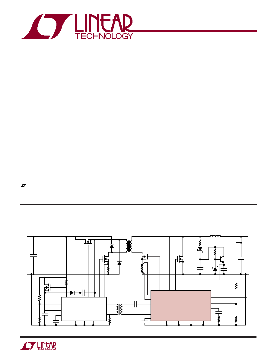
36V-72V to 3.3V/20A Isolated Forward Converter
The LTC
®
3726 is a secondary-side controller for synchro-
nous forward converters. When used in conjunction with
the LTC3705/LTC3725 gate driver and primary-side con-
trollers, the part creates a complete isolated power supply
that combines the simplicity of OPTI-LOOP
®
compensa-
tion with the speed of secondary-side control.
The LTC3726 has been designed to simplify the design of
highly efficient, secondary-side forward converters. Work-
ing in concert with the LTC3705 or LTC 3725, the LTC3726
forms a robust, self-starting converter that eliminates the
need for the separate bias regulator that is commonly used
in secondary-side control applications. In addition, a pro-
prietary scheme is used to multiplex gate drive signals and
DC bias power across the isolation barrier through a
single, tiny pulse transformer.
The LTC3726 is available in a 16-lead SSOP package.
NDRV
GND
PGND VSLMT
UVLO
BOOST
LTC3705
BAS21
FQT7N10
0.22
µF
10
µF
25V
CMPSH1-4
1.2
L1
1.2
µH
TG
TS BG IS
T2
1
µF
162k
L1: COILCRAFT SER2010-122
T1: PULSE PA0807
T2: PULSE PA0297
33nF
30m
1W
2m
2W
Si7336ADP
Si7336ADP
×2
T1
·
·
MURS120
Si7852DP
Si7852DP
MURS120
V
CC
33nF
15k
1%
365k
1%
100k
2.2
µF
25V
SS/FLT
FB/IN
+
FS/IN
V
IN
V
IN
+
330
µF
6.3V
×3
680pF
22.6k
1%
20k
102k
1%
V
OUT
3726 TA01
V
OUT
+
·
·
1
µF
100V
x3
FG
SW SG
V
CC
GND
PGND
SLP
MODE
PT
+
I
S
+
I
S
PT
RUN/SS
LTC3726
ITH
FB/PHASE
FS/SYNC
7.5V
2.2
µF
FZT690B
5k
2
LTC3726
3726f
(Note 1)
V
CC
........................................................... 0.3V to 10V
SW ............................................................... 5V to 50V
ITH, RUN/SS ............................................... 0.3V to 7V
All Other Pins ............................................ 0.3V to 10V
Operating Ambient Temperature Range (Note 2)
LTC3726EGN ...................................... 40
°C to 85°C
LTC3726IGN ....................................... 40
°C to 85°C
Operating Junction Temperature (Note 3) ........... 125
°C
Storage Temperature Range ................. 65
°C to 150°C
Lead Temperature (Soldering, 10 sec).................. 300
°C
ABSOLUTE
M
AXI
M
U
M
RATINGS
W
W
W
U
PACKAGE/ORDER I
N
FOR
M
ATIO
N
W
U
U
The
indicates specifications which apply over the full operating
temperature range, otherwise specifications are at T
A
= 25
°C. V
CC
= 7V, GND = PGND = 0V, unless otherwise noted.
ELECTRICAL CHARACTERISTICS
SYMBOL
PARAMETER
CONDITIONS
MIN
TYP
MAX
UNITS
Main Control Loop
V
FB
Regulated Feedback Voltage
(Note 4) ITH = 1.2V
0.594
0.600
0.606
V
V
FB(LINREG)
Feedback Voltage Line Regulation
V
CC
= 5V to 10V, ITH = 1.2V
0.001
%/V
V
FB(LOADREG)
Feedback Voltage Load Regulation
Measured in Servo Loop,
0.01
0.1
%
ITH = 0.5V to 2V
V
ISMAX
Maximum Current Sense Threshold
R
SENSE
Mode, 0V < V
IS
< 5V
68
78
88
mV
V
IS
= V
CC
, 0V < V
IS
+
< 2V (CT Mode)
1.15
1.28
1.4
V
V
ISOC
Over-Current Shutdown Threshold
R
SENSE
Mode, 0V < V
IS
< 5V
87
100
113
mV
V
IS
= V
CC
, 0V < V
IS
+
< 2V (CT Mode)
1.45
1.65
1.85
V
g
m
Transconductance Amplifier g
m
2.40
2.75
3.10
mS
I
RUN/SS(C)
Soft-Start Charge Current
V
RUN/SS
= 2V
4
5
6
µA
I
RUN/SS(D)
Soft-Start Discharge Current
3
µA
V
RUN/SS
RUN/SS Pin ON Threshold
V
RUN/SS
Rising
0.4
0.45
0.5
V
t
ON,MIN
Minimum ON Time
200
ns
FG, SG R
UP
FG, SG Driver Pull-Up On Resistance
FG, SG Low
1.5
2.3
FG, SG R
DOWN
FG, SG Driver Pull-Down On Resistance
FG, SG High
1.5
2.3
PT
+
, PT
R
UP
PT
+
, PT
Driver Pull-Up Resistance
PT
+
, PT
Low
1.5
2.3
PR
+
, PT
R
DOWN
PT
+
, PT
Driver Pull-Down Resistance
PT
+
, PT
High
1.5
2.3
V
FB(OV)
Output Overvoltage Threshold
V
FB
Rising
15
17
19
%
Order Options Tape and Reel: Add #TR
Lead Free: Add #PBF Lead Free Tape and Reel: Add #TRPBF
Lead Free Part Marking: http://www.linear.com/leadfree/
Consult LTC Marketing for parts specified with wider operating temperature ranges.
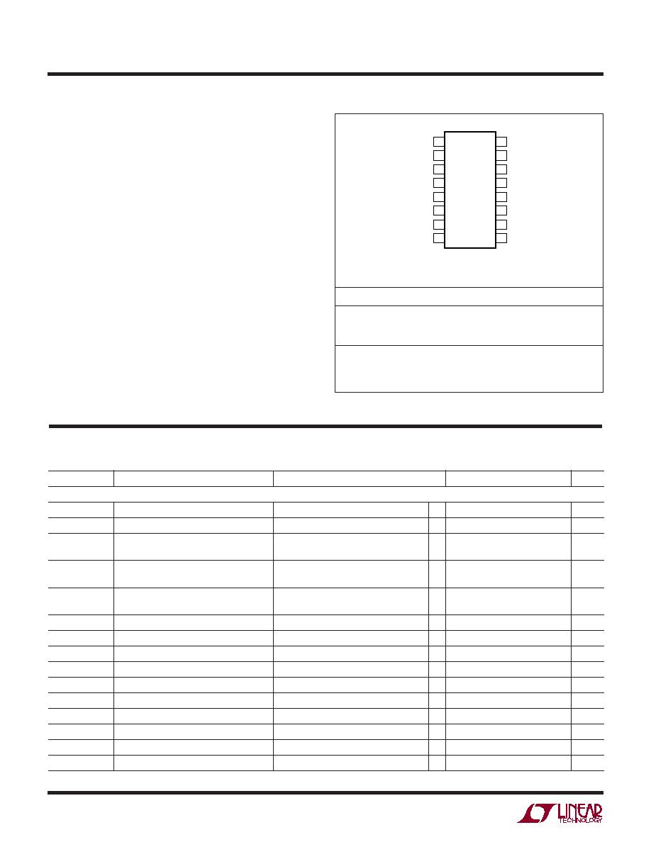
GN PACKAGE
16-LEAD PLASTIC SSOP
1
2
3
4
5
6
7
8
TOP VIEW
16
15
14
13
12
11
10
9
SG
FG
MODE
FB/PHASE
ITH
RUN/SS
SLP
GND
V
CC
PT
+
PT
PGND
SW
IS
+
IS
FS/SYNC
T
JMAX
= 125
°C,
JA
= 130
°C/W
ORDER PART NUMBER
LTC3726EGN
LTC3726IGN
3
LTC3726
3726f
The
indicates specifications which apply over the full operating
temperature range, otherwise specifications are at T
A
= 25
°C. V
CC
= 7V, GND = PGND = 0V, unless otherwise noted.
ELECTRICAL CHARACTERISTICS
Note 1: Stresses beyond those listed under Absolute Maximum Ratings
may cause permanent damage to the device. Exposure to any Absolute
Maximum Rating condition for extended periods may affect device
reliability and lifetime.
Note 2: The LTC3726EGN is guaranteed to meet performance
specifications from 0
°C to 85°C operating temperature range are assured
by design, characterization and correlation with statistical process
controls. The LTC3726IGN is guaranteed and tested over the 40
°C to
85
°C operating temperature range.
Note 3: Operating junction temperature T
J
(in
°C) is calculated from the
ambient temperature T
A
and the average power dissipation P
D
(in Watts)
by the formula:
T
J
= T
A
+
JA
· P
D
Refer to the Applications Information section for details.
Note 4: The LTC3726 is tested in a feedback loop that servos V
FB
to a
voltage near the internal 0.6V reference voltage to obtain the specified ITH
voltage (V
ITH
= 1.2V).
Note 5: Operating supply current is measured in test mode. Dynamic
supply current is higher due to the internal gate charge being delivered at
the switching frequency. See Typical Performance Characteristics.
SYMBOL
PARAMETER
CONDITIONS
MIN
TYP
MAX
UNITS
V
CC
Supply
V
CCOP
Operating Voltage Range
5
10
V
I
CC
Supply Current
Operating
f
OSC
= 200kHz (Note 5)
4.2
mA
Shutdown
V
RUN/SS
= GND
700
µA
V
UVLO
UV Lockout
V
CC
Rising
4.52
4.60
4.70
V
V
HYS
UV Hysteresis
0.4
V
Oscillator and Phase-Locked Loop
I
FS
FS/SYNC Pin Sourcing Current
20
µA
f
LOW
Oscillator Low Frequency Set Point
V
FS/SYNC
= GND
170
200
230
kHz
f
HIGH
Oscillator High Frequency Set Point
V
FS/SYNC
= V
CC
255
300
345
kHz
f (R
FS
)
Oscillator Resistor Set Accuracy
75k
< R
FS/SYNC
< 175k
20
20
%
f
PLL(MAX)
Maximum PLL Sync Frequency
500
kHz
f
PLL(MIN)
Minimum PLL Sync Frequency
75
kHz
4
LTC3726
3726f
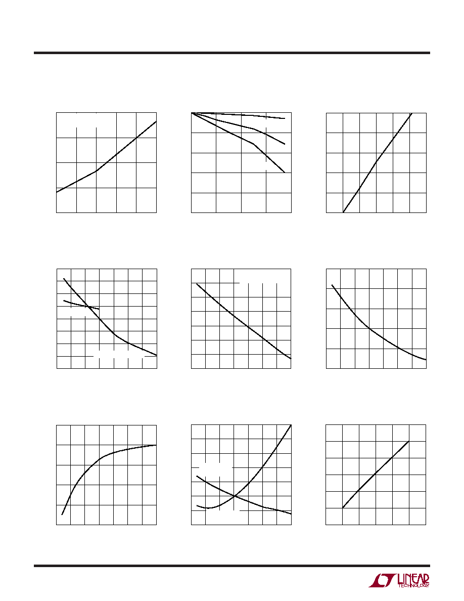
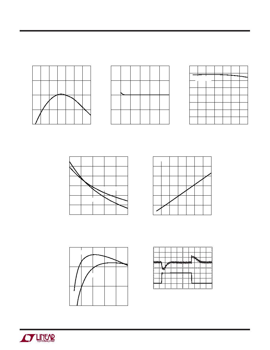
TYPICAL PERFOR A CE CHARACTERISTICS
U
W
V
CC
Supply Current vs
Input Voltage
Maximum Current Sense
Threshold vs Duty Cycle
Maximum Current Sense
Threshold vs ITH Voltage
IS Pins Source Current
IS Pins Source Current
vs Temperature
Maximum Current Sense
Threshold vs Temperature
RUN/SS ON Threshold
vs Temperature
Oscillator Frequency
vs Temperature
INPUT VOLTAGE (V)
5
5
6
7
9
8
3726 G01
4
6
7
10
3
SUPPLY CURRENT (mA)
f
OSC
= 200kHz
ALL GATES: C
LOAD
= 0
DUTY CYCLE (%)
0
60
80
100
60
3726 G03
40
20
20
40
80
0
R
SLP
= 0
R
SLP
= 50k
100k
V
IS
/V
IS,MAX
(%)
ITH VOLTAGE (V)
0
60
80
100
2.0
2.5
1.5
3726 G04
40
20
0.5
1.0
3.0
0
V
IS
/V
IS,MAX
(%)
IS
+
, IS
COMMON-MODE VOLTAGE (V)
1
100
100
400
300
200
0
3
4
2
3726 G05
200
300
0
1
6
5
400
IS PIN SOURCE CURRENT (
µ
A)
RS-MODE: (I
IS
+ + I
IS
)
CT-MODE: I
IS
+
240
250
265
260
255
245
3726 G06
235
230
IS PIN SOURCE CURRENT (
µ
A)
TEMPERATURE (
°C)
50
50
75
100
25
25
0
125
RS-MODE: (I
IS
+ + I
IS
)
V
IS
+ = V
IS
= 0V
100.0
101.5
101.0
100.5
99.5
3726 G07
99.0
V
IS
/V
IS,MAX
(%)
TEMPERATURE (
°C)
50
50
75
100
25
25
0
125
440
470
460
450
430
3726 G08
420
V
RUN/SS
(mV)
TEMPERATURE (
°C)
50
50
75
100
25
25
0
125
0
2
5
4
3
1
3726 G14
1
2
PERCENT CHANGE IN FREQUENCY (%)
TEMPERATURE (
°C)
50
50
75
100
25
25
0
125
R = 175K
f
OSC
= 500kHz
R = 75K
f
OSC
= 100kHz
T
A
= 25
°C, unless otherwise noted.
Oscillator Frequency vs R
FS
R
FS
(k
)
50
400
500
600
150
175
125
3726 G09
300
200
100
75
100
200
0
FREQUENCY (kHz)
5
LTC3726
3726f
TYPICAL PERFOR A CE CHARACTERISTICS
U
W
FB Voltage vs Temperature
FB Voltage Line Regulation
Undervoltage Lockout
vs Temperature
Gate Driver On-Resistance vs V
CC
Gate Driver On-Resistance
vs Temperature
Efficiency (Figure 5)
Load Step (Figure 5)
V
IN
SUPPLY VOLTAGE (V)
0
600.0
600.5
601.0
20
25
15
3726 G11
599.5
5
10
30
599.0
V
FB
(mV)
V
CC
VOLTAGE (V)
5
1.6
1.7
1.8
9
8
3726 G12
1.5
1.4
1.3
6
7
10
1.2
R
DS,ON
(
)
PULL-DOWN
PULL-UP
1.25
1.75
2.50
2.25
2.00
1.50
3726 G13
1.00
R
DS,ON
(
)
TEMPERATURE (
°C)
50
50
75
100
25
25
0
125
V
CC
= 7V
599.5
601.0
600.5
600.0
3726 G15
599.0
V
FB
(mV)
TEMPERATURE (
°C)
50
50
75
100
25
25
0
125
4.40
4.50
4.65
4.60
4.55
4.45
3726 G16
4.35
4.30
4.25
UVLO THRESHOLD VOLTAGE (V)
TEMPERATURE (
°C)
50
50
75
100
25
25
0
125
V
CC
RISING
LOAD CURRENT (A)
0
85
90
95
20
15
3726 G17
5
10
25
80
EFFICIENCY (%)
V
IN
= 36V
V
IN
= 72V
20
µs/DIV
V
IN
= 48V
V
OUT
= 3.3V
LOAD STEP = 0A TO 20A
V
OUT
100mV/DIV
I
OUT
10A/DIV
3726 G18