Äîêóìåíòàöèÿ è îïèñàíèÿ www.docs.chipfind.ru

1
LTC3729
sn3729 3729fas
550kHz, PolyPhase,
High Efficiency, Synchronous
Step-Down Switching Regulator
, LTC and LT are registered trademarks of Linear Technology Corporation.
OPTI-LOOP is a registered trademark of Linear Technology Corporation.
PolyPhase is a trademark of Linear Technology Corporation.
The LTC
®
3729 is a multiple phase, synchronous step-
down current mode switching regulator controller that
drives N-channel external power MOSFET stages in a
phase-lockable fixed frequency architecture. The PolyPhase
controller drives its two output stages out of phase at
frequencies up to 550kHz to minimize the RMS ripple
currents in both input and output capacitors. The output
clock signal allows expansion for up to 12 evenly phased
controllers for systems requiring 15A to 200A of output
current. The multiple phase technique effectively multi-
plies the fundamental frequency by the number of chan-
nels used, improving transient response while operating
each channel at an optimum frequency for efficiency.
Thermal design is also simplified.
An internal differential amplifier provides true remote
sensing of the regulated supply's positive and negative
output terminals as required for high current applications.
A RUN/SS pin provides both soft-start and optional timed,
short-circuit shutdown. Current foldback limits MOSFET
dissipation during short-circuit conditions when the
overcurrent latchoff is disabled. OPTI-LOOP compensa-
tion allows the transient response to be optimized over a
wide range of output capacitance and ESR values. The
LTC3729 includes a power good output pin that indicates
when the output is within
±
7.5% of the designed set point.
Figure 1. High Current Dual Phase Step-Down Converter
s
Desktop Computers/Servers
s
Large Memory Arrays
s
DC Power Distribution Systems
s
Wide V
IN
Range: 4V to 36V Operation
s
Reduces Required Input Capacitance and Power
Supply Induced Noise
s
±
1% Output Voltage Accuracy
s
Phase-Lockable Fixed Frequency: 250kHz to 550kHz
s
True Remote Sensing Differential Amplifier
s
PolyPhase
TM
Extends from Two to Twelve Phases
s
Reduces the Size and Value of Inductors
s
Current Mode Control Ensures Current Sharing
s
1.1MHz Effective Switching Frequency (2-Phase)
s
OPTI-LOOP
®
Compensation Reduces C
OUT
s
Power Good Output Voltage Indicator
s
Very Low Dropout Operation: 99% Duty Cycle
s
Adjustable Soft-Start Current Ramping
s
Internal Current Foldback Plus Shutdown Timer
s
Overvoltage Soft-Latch Eliminates Nuisance Trips
s
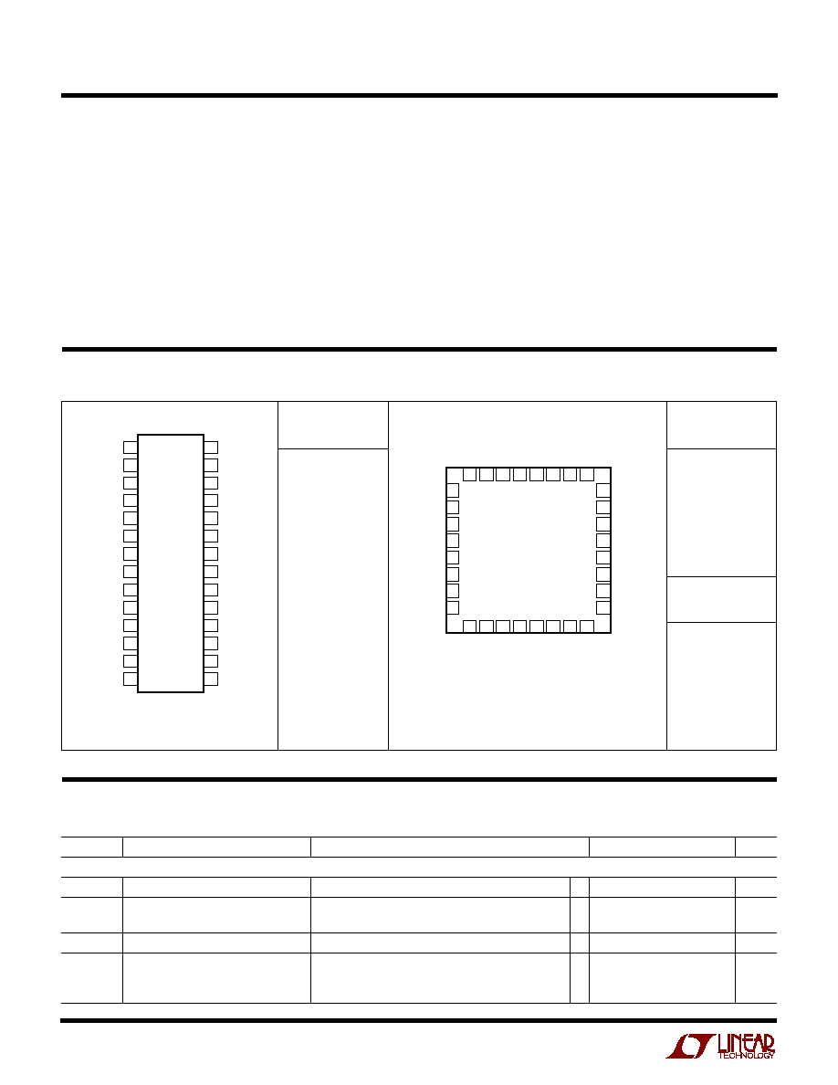
Available in 5mm
×
5mm QFN
and 28-Lead SSOP Packages
3729 TA01
TG1
BOOST1
SW1
BG1
PGND
SENSE1
+
SENSE1
TG2
BOOST2
SW2
BG2
INTV
CC
SENSE2
+
SENSE2
V
IN
RUN/SS
EAIN
I
TH
V
DIFFOUT
V
OS
V
OS
+
LTC3729
SGND
0.1
µ
F
PGOOD
0.1
µ
F
16k
1000pF
S
S
S
S
S
S
S
S
10
3.3k
16k
+
10
µ
F
35V
CERAMIC
×
4
+
C
OUT
1000
µ
F
×
2
4V
L1, L2: CEPH149-IROMC
C
OUT
: T510E108K004AS
D1, D2: UP5840
M1, M3: IRF7811W
M2, M4: IRF7822
V
OUT
1.6V/40A
L1
0.8
µ
H
0.002
V
IN
5V TO 28V
L2
0.8
µ
H
D2
D1
M1
M2
×
2
M3
M4
×
2
0.47
µ
F
S
0.47
µ
F
10
µ
F
0.002
APPLICATIO S
U
FEATURES
TYPICAL APPLICATIO
U
DESCRIPTIO
U
2
LTC3729
sn3729 3729fas
ORDER PART
NUMBER
LTC3729EG
ABSOLUTE AXI U
RATI GS
W
W
W
U
PACKAGE/ORDER I FOR ATIO
U
U
W
T
JMAX
= 125
°
C,
JA
= 95
°
C/W
(Note 1)
Input Supply Voltage (V
IN
).........................36V to 0.3V
Topside Driver Voltages (BOOST1,2) .........42V to 0.3V
Switch Voltage (SW1, 2) .............................36V to 5 V
SENSE1
+
, SENSE2
+
, SENSE1
,
SENSE2
Voltages ........................ (1.1)INTV
CC
to 0.3V
EAIN, V
OS
+
, V
OS
, EXTV
CC
, INTV
CC
,
RUN/SS, PGOOD Voltages ...........................7V to 0.3V
Boosted Driver Voltage (BOOST-SW) .......... 7V to 0.3V
PLLFLTR, PLLIN, CLKOUT, PHASMD,
V
DIFFOUT
Voltages ................................ INTV
CC
to 0.3V
1
2
3
4
5
6
7
8
9
10
11
12
13
14
TOP VIEW
G PACKAGE
28-LEAD PLASTIC SSOP
28
27
26
25
24
23
22
21
20
19
18
17
16
15
RUN/SS
SENSE1
+
SENSE1
EAIN
PLLFLTR
PLLIN
PHASMD
I
TH
SGND
V
DIFFOUT
V
OS
V
OS
+
SENSE2
SENSE2
+
CLKOUT
TG1
SW1
BOOST1
V
IN
BG1
EXTV
CC
INTV
CC
PGND
BG2
BOOST2
SW2
TG2
PGOOD
I
TH
Voltage ................................................ 2.7V to 0.3V
Peak Output Current <1
µ
s(TGL1,2, BG1,2) ................ 5A
INTV
CC
RMS Output Current ................................ 50mA
Operating Ambient Temperature
Range (Note 6) ................................... 40
°
C to 85
°
C
Junction Temperature (Note 2) ............................. 125
°
C
Storage Temperature Range ................. 65
°
C to 150
°
C
Lead Temperature (Soldering, 10 sec)
(G Package Only) .................................................. 300
°
C
32 31 30 29 28 27 26 25
9
10 11 12 13
TOP VIEW
UH PACKAGE
32-LEAD 5mm
×
5mm PLASTIC QFN
14 15 16
17
18
19
20
21
22
23
24
8
7
6
5
4
3
2
1
EAIN
PLLFLTR
PLLIN
PHASMD
I
TH
SGND
V
DIFFOUT
V
OS
BOOST1
V
IN
BG1
EXTV
CC
INTV
CC
PGND
BG2
BOOST2
NC
SENSE1
SENSE1
+
NC
RUN/SS
CLKOUT
TG1
SW1
V
OS
+
NC
SENSE2
SENSE2
+
PGOOD
TG2
SW2
NC
ORDER PART
NUMBER
LTC3729EUH
ELECTRICAL CHARACTERISTICS
The
q
denotes the specifications which apply over the full operating
temperature range, otherwise specifications are at T
A
= 25
°
C. V
IN
= 15V, V
RUN/SS
= 5V unless otherwise noted.
SYMBOL
PARAMETER
CONDITIONS
MIN
TYP
MAX
UNITS
Main Control Loop
V
EAIN
Regulated Feedback Voltage
(Note 3); I
TH
Voltage = 1.2V
q
0.792
0.800
0.808
V
V
SENSEMAX
Maximum Current Sense Threshold
V
SENSE
= 5V
q
62
75
88
mV
V
SENSE1, 2
= 5V
65
75
85
mV
I
INEAIN
Feedback Current
(Note 3)
5
50
nA
V
LOADREG
Output Voltage Load Regulation
(Note 3)
Measured in Servo Loop; I
TH
Voltage = 0.7V
q
0.1
0.5
%
Measured in Servo Loop; I
TH
Voltage = 2V
q
0.1
0.5
%
Consult LTC Marketing for parts specified with wider operating temperature ranges.
JA
= 34
°
C/W
EXPOSED PAD IS SGND
(MUST BE SOLDERED TO PCB)
UH PART
MARKING
3729

3
LTC3729
sn3729 3729fas
SYMBOL
PARAMETER
CONDITIONS
MIN
TYP
MAX
UNITS
ELECTRICAL CHARACTERISTICS
The
q
denotes the specifications which apply over the full operating
temperature range, otherwise specifications are at T
A
= 25
°
C. V
IN
= 15V, V
RUN/SS
= 5V unless otherwise noted.
V
REFLNREG
Reference Voltage Line Regulation
V
IN
= 3.6V to 30V (Note 3)
0.002
0.02
%/V
V
OVL
Output Overvoltage Threshold
Measured at V
EAIN
q
0.84
0.86
0.88
V
UVLO
Undervoltage Lockout
V
IN
Ramping Down
3
3.5
4
V
g
m
Transconductance Amplifier g
m
I
TH
= 1.2V; Sink/Source 5
µ
A; (Note 3)
3
mmho
g
mOL
Transconductance Amplifier Gain
I
TH
= 1.2V; (g
m
xZ
L
; No Ext Load); (Note 3)
1.5
V/mV
I
Q
Input DC Supply Current
(Note 4)
Normal Mode
EXTV
CC
Tied to V
OUT
; V
OUT
= 5V
580
µ
A
Shutdown
V
RUN/SS
= 0V
20
40
µ
A
I
RUN/SS
Soft-Start Charge Current
V
RUN/SS
= 1.9V
0.5
1.2
µ
A
V
RUN/SS
RUN/SS Pin ON Threshold
V
RUN/SS
Rising
1.0
1.5
1.9
V
V
RUN/SSLO
RUN/SS Pin Latchoff Arming
V
RUN/SS
Rising from 3V
3.8
4.5
V
I
SCL
RUN/SS Discharge Current
Soft Short Condition V
EAIN
= 0.5V; V
RUN/SS
= 4.5V
0.5
2
4
µ
A
I
SDLDO
Shutdown Latch Disable Current
V
EAIN
= 0.5V
1.6
5
µ
A
I
SENSE
Total Sense Pins Source Current
Each Channel; V
SENSE1
, 2
= V
SENSE1
+
, 2
+ = 0V
85
60
µ
A
DF
MAX
Maximum Duty Factor
In Dropout
98
99.5
%
Top Gate Transition Time:
TG1, 2 t
r
Rise Time
C
LOAD
= 3300pF
30
90
ns
TG1, 2 t
f
Fall Time
C
LOAD
= 3300pF
40
90
ns
Bottom Gate Transition Time:
BG1, 2 t
r
Rise Time
C
LOAD
= 3300pF
30
90
ns
BG1, 2 t
f
Fall Time
C
LOAD
= 3300pF
20
90
ns
TG/BG t
1D
Top Gate Off to Bottom Gate On Delay
Synchronous Switch-On Delay Time
C
LOAD
= 3300pF Each Driver
90
ns
BG/TG t
2D
Bottom Gate Off to Top Gate On Delay
Top Switch-On Delay Time
C
LOAD
= 3300pF Each Driver
90
ns
t
ON(MIN)
Minimum On-Time
Tested with a Square Wave (Note 5)
100
ns
Internal V
CC
Regulator
V
INTVCC
Internal V
CC
Voltage
6V < V
IN
< 30V; V
EXTVCC
= 4V
4.8
5.0
5.2
V
V
LDO
INT
INTV
CC
Load Regulation
I
CC
= 0 to 20mA; V
EXTVCC
= 4V
0.2
1.0
%
V
LDO
EXT
EXTV
CC
Voltage Drop
I
CC
= 20mA; V
EXTVCC
= 5V
80
160
mV
V
EXTVCC
EXTV
CC
Switchover Voltage
I
CC
= 20mA, EXTV
CC
Ramping Positive
q
4.5
4.7
V
V
LDOHYS
EXTV
CC
Switchover Hysteresis
I
CC
= 20mA, EXTV
CC
Ramping Negative
0.2
V
Oscillator and Phase-Locked Loop
f
NOM
Nominal Frequency
V
PLLFLTR
= 1.2V
360
400
440
kHz
f
LOW
Lowest Frequency
V
PLLFLTR
= 0V
230
260
290
kHz
f
HIGH
Highest Frequency
V
PLLFLTR
2.4V
480
550
590
kHz
R
PLLIN
PLLIN
Input Resistance
50
k
I
PLLFLTR
Phase Detector Output Current
Sinking Capability
f
PLLIN
< f
OSC
15
µ
A
Sourcing Capability
f
PLLIN
> f
OSC
15
µ
A
R
RELPHS
Controller 2-Controller 1 Phase
V
PHASMD
= 0V, Open
180
Deg
V
PHASMD
= 5V
240
Deg

4
LTC3729
sn3729 3729fas
ELECTRICAL CHARACTERISTICS
The
q
denotes the specifications which apply over the full operating
temperature range, otherwise specifications are at T
A
= 25
°
C. V
IN
= 15V, V
RUN/SS
= 5V unless otherwise noted.
Note 4: Dynamic supply current is higher due to the gate charge being
delivered at the switching frequency. See Applications Information.
Note 5: The minimum on-time condition corresponds to the on inductor
peak-to-peak ripple current
40% of I
MAX
(see Minimum On-Time
Considerations in the Applications Information section).
Note 6: The LTC3729E is guaranteed to meet performance specifications
from 0
°
C to 70
°
C. Specifications over the 40
°
C to 85
°
C operating
temperature range are assured by design, characterization and correlation
with statistical process controls.
Note 1: Absolute Maximum Ratings are those values beyond which the
life of a device may be impaired.
Note 2: T
J
is calculated from the ambient temperature T
A
and power
dissipation P
D
according to the following formulas:
LTC3729EG: T
J
= T
A
+ (P
D
· 95
°
C/W)
LTC3729EUH: T
J
= T
A
+ (P
D
· 34
°
C/W)
Note 3: The LTC3729 is tested in a feedback loop that servos V
ITH
to a
specified voltage and measures the resultant V
EAIN
.
TYPICAL PERFOR A CE CHARACTERISTICS
U
W
Efficiency vs Output Current
(Figure 12)
Efficiency vs Output Current
(Figure 12)
Efficiency vs Input Voltage
(Figure 12)
OUTPUT CURRENT (A)
0.1
EFFICIENCY (%)
100
80
60
40
20
0
3729 G01
1
10
100
V
OUT
= 3.3V
V
EXTVCC
= 5V
I
OUT
= 20A
f = 250kHz
V
IN
= 5V
V
IN
= 8V
V
IN
= 12V
V
IN
= 20V
OUTPUT CURRENT (A)
1
EFFICIENCY (%)
70
80
3729
G02
60
50
10
100
100
90
V
EXTVCC
= 0V
V
OUT
= 3.3V
f = 250kHz
V
EXTVCC
= 5V
V
IN
(V)
5
EFFICIENCY (%)
100
90
80
70
3729 G03
10
15
20
V
OUT
= 3.3V
V
EXTVCC
= 5V
I
OUT
= 20A
f = 250kHz
SYMBOL
PARAMETER
CONDITIONS
MIN
TYP
MAX
UNITS
CLKOUT
Phase (Relative to Controller 1)
V
PHASMD
= 0V
60
Deg
V
PHASMD
= Open
90
Deg
V
PHASMD
= 5V
120
Deg
CLK
HIGH
Clock High Output Voltage
4
V
CLK
LOW
Clock Low Output Voltage
0.2
V
PGOOD Output
V
PGL
PGOOD Voltage Low
I
PGOOD
= 2mA
0.1
0.3
V
I
PGOOD
PGOOD Leakage Current
V
PGOOD
= 5V
±
1
µ
A
V
PG
PGOOD Trip Level, Either Controller
V
EAIN
with Respect to Set Output Voltage
V
EAIN
Ramping Negative
6
7.5
9.5
%
V
EAIN
Ramping Positive
6
7.5
9.5
%
Differential Amplifier
A
DA
Gain
0.995
1
1.005
V/V
CMRR
DA
Common Mode Rejection Ratio
0V < V
CM
< 5V
46
55
dB
R
IN
Input Resistance
Measured at V
OS
+ Input
80
k
5
LTC3729
sn3729 3729fas
Internal 5V LDO Line Reg
Maximum Current Sense Threshold
vs Duty Factor
Maximum Current Sense Threshold
vs Percent of Nominal Output
Voltage (Foldback)
Maximum Current Sense Threshold
vs V
RUN/SS
(Soft-Start)
Maximum Current Sense Threshold
vs Sense Common Mode Voltage
Current Sense Threshold
vs I
TH
Voltage
INTV
CC
and EXTV
CC
Switch
Voltage vs Temperature
Supply Current vs Input Voltage
and Mode
EXTV
CC
Voltage Drop
TYPICAL PERFOR A CE CHARACTERISTICS
U
W
INPUT VOLTAGE (V)
0
5
0
SUPPLY CURRENT (
µ
A)
400
1000
10
20
25
3729 G04
200
800
600
15
30
35
ON
SHUTDOWN
CURRENT (mA)
0
EXTV
CC
VOLTAGE DROP (mV)
150
200
250
40
3729 G05
100
50
0
10
20
30
50
TEMPERATURE (
°
C)
50
INTV
CC
AND EXTV
CC
SWITCH VOLTAGE (V)
4.95
5.00
5.05
25
75
3729 G06
4.90
4.85
25
0
50
100
125
4.80
4.70
4.75
INTV
CC
VOLTAGE
EXTV
CC
SWITCHOVER THRESHOLD
INPUT VOLTAGE (V)
0
4.8
4.9
5.1
15
25
3729 G07
4.7
4.6
5
10
20
30
35
4.5
4.4
5.0
INTV
CC
VOLTAGE (V)
I
LOAD
= 1mA
DUTY FACTOR (%)
0
0
V
SENSE
(mV)
25
50
75
20
40
60
80
3729 G08
100
PERCENT ON NOMINAL OUTPUT VOLTAGE (%)
0
V
SENSE
(mV)
40
50
60
100
3729 G09
30
20
0
25
50
75
10
80
70
V
RUN/SS
(V)
0
0
V
SENSE
(mV)
20
40
60
80
1
2
3
4
3729 G10
5
6
V
SENSE(CM)
= 1.6V
COMMON MODE VOLTAGE (V)
0
V
SENSE
(mV)
72
76
80
4
3729 G11
68
64
60
1
2
3
5
V
ITH
(V)
0
V
SENSE
(mV)
30
50
70
90
2
3729 G12
10
10
20
40
60
80
0
20
30
0.5
1
1.5
2.5