Äîêóìåíòàöèÿ è îïèñàíèÿ www.docs.chipfind.ru
1
LTC3738
3738f
APPLICATIO S
U
FEATURES
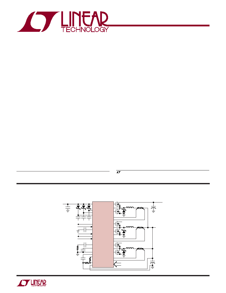
TYPICAL APPLICATIO
U
DESCRIPTIO
U
3-Phase Buck Controller
for Intel VRM9/VRM10 with
Active Voltage Positioning
, LTC and LT are registered trademarks of Linear Technology Corporation.
OPTI-LOOP is a registered trademark of Linear Technology Corporation.
Stage Shedding is a trademark of Linear Technology Corporation.
3-Phase Controller with Onboard MOSFET Drivers
Programmable Active Voltage Positioning (AVP)
with True Current Sensing
Programmable External Thermal Detection or
Internal Thermal Sensing
Precise Output Current Matching Optimizes
Thermal Performance and Solution Size
Supports Starting into Precharged V
OUTS
Differential Amplifier Accurately Senses V
OUT
PWM, Pulse Skip and Stage Shedding
TM
Operation
Synchronizable
210kHz to 530kHz Per Phase, Fixed Frequency
Output Power Good Indicator with Adaptive Blanking
Adjustable Soft-Start Current Ramping
Short-Circuit Shutdown Timer with Defeat Option
OPTI-LOOP
®
Compensation Minimizes C
OUT
38-Lead (5mm × 7mm) QFN Package
High Performance Notebook Computers
Servers, Desktop Computers and Workstations
VRM10 Step-Down Controller
The LTC
®
3738 is a 3-phase synchronous step-down switch-
ing regulator controller that drives all N-channel external
power MOSFET stages in a phase-lockable, fixed fre-
quency architecture. The 3-phase technique effectively
triples the fundamental frequency, improving transient
response while operating each controller at an optimal
frequency for efficiency and ease of thermal design. Light
load efficiency is optimized by using a choice of output
Stage Shedding or Pulse Skip mode technology.
The LTC3738 also allows users to program load slope via
a resistor for AVP control. Both external and internal
thermal sensing are available from the on-chip thermal
detector and comparator.
A differential amplifier provides sensing of both the high
and low sides of the output voltage.
Soft-start and a defeatable, timed short-circuit shutdown
protect the MOSFETs and the load. A foldback current
circuit also provides protection for the external MOSFETs
under short-circuit or overload conditions. An all- "1" VID
detector turns off the regulator after a 1µs timeout.
0.002
0.8µH
22µF
×2
0.002
0.8µH
V
IN
0.002
470µF
×4
V
OUT
0.8375V TO 1.6000V
V
IN
5V TO 28V
0.8µH
V
IN
6 VID BITS
3738 TA01
TG1
V
CC
0.1µF
SW3 SW2 SW1
SW1
BG1
SENSE1
+
SENSE1
BOOST1
BOOST2
BOOST3
TG2
SW2
BG2
PGOOD
OUTEN
PLLFLTR
I
TH
0.1µF
100pF
680pF
5k
ON/OFF
POWER GOOD INDICATOR
SS
SGND
EAIN
AVP
PGND
SENSE2
+
SENSE2
TG3
SW3
BG3
VID0-VID5
SENSE3
+
SENSE3
IN
+
IN
FCB/SYNC
MODE SELECTION/SYNC IN
TSNS
THERMAL INPUT
VR_HOTB
VR HOT INDICATOR
+
10µF
5V
+
LTC3738
U.S. Patent Numbers: 5481178, 5994885, 5929620, 6177787, 6144194, 6580258, 6462525,
6593724, 6674274, 6100678 pending on AVP technique.
2
LTC3738
3738f
ABSOLUTE AXI U RATI GS
W
W
W
U
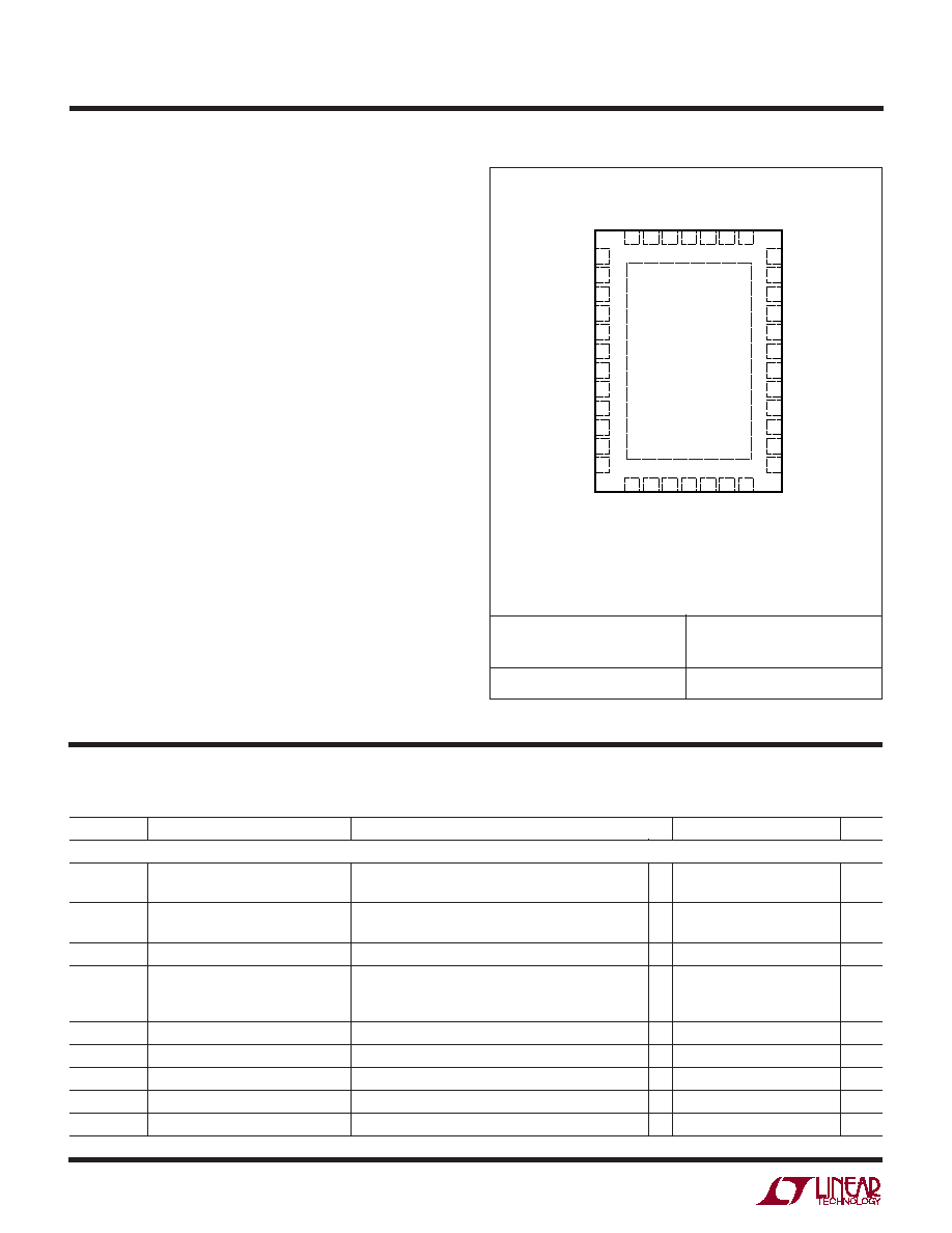
PACKAGE/ORDER I FOR ATIO
U
U
W
Topside Driver Voltages (BOOST
N
) ............ 38V to 0.3V
Switch Voltage (SW
N
)................................... 32V to 5V
Boosted Driver Voltage (BOOST
N
SW
N
) .... 7V to 0.3V
Peak Output Current <1ms (TG
N
, BG
N
) ..................... 5A
Supply Voltage (V
CC
), PGOOD, VR_HOTB
Pin Voltages ................................................ 7V to 0.3V
OUTEN, SS, PLLFLTR,
FCB/SYNC Voltages ................................... V
CC
to 0.3V
I
TH
Voltage ................................................ 2.4V to 0.3V
IN
+
, IN
, VID0-VID5, TSNS .............................. 5V to 0V
AVP, SENSE
+
, SENSE
.................................. 1.9V to 0V
Operating Ambient Temperature Range ....... 0°C to 85°C
Junction Temperature (Note 2) ............................. 125°C
Storage Temperature Range ..................65°C to 125°C
Consult LTC Marketing for parts specified with wider operating temperature ranges.
(Note 1)
ORDER PART
NUMBER
LTC3738CUHF
13 14 15 16
TOP VIEW
39
UHF PACKAGE
38-LEAD (7mm × 5mm) PLASTIC QFN
17 18 19
38 37 36 35 34 33 32
24
25
26
27
28
29
30
31
8
7
6
5
4
3
2
1
FCB/SYNC
PLLFLTR
IN
IN
+
AVP
EAIN
SENSE1
+
SENSE1
SENSE2
+
SENSE2
SENSE3
SENSE3
+
TG1
SW1
BOOST2
TG2
SW2
V
CC
BG1
PGND
BG2
BG3
SW3
TG3
OUTEN
VID2
VID1
VID0
VID5
PGOOD
BOOST1
SS
I
TH
TSNS
VR_HOTB
VID3
VID4
BOOST3
23
22
21
20
9
10
11
12
T
JMAX
= 125°C,
JA
= 34°C/W
EXPOSED PAD (PIN 39) IS SGND MUST BE SOLDERED TO PCB
ELECTRICAL CHARACTERISTICS
The
denotes the specifications which apply over the full operating
temperature range, otherwise specifications are at T
A
= 25°C. V
CC
= V
OUTEN
= V
SS
= 5V unless otherwise noted.
SYMBOL
PARAMETER
CONDITIONS
MIN
TYP
MAX
UNITS
Main Control Loop
V
REGULATED
Regulated Voltage at IN
+
(Note 3); VID Code = 110101, V
ITH
= 1.2V
1.166
1.175
1.184
V
1.163
1.175
1.187
V
V
SENSEMAX
Maximum Current Sense Threshold
V
EAIN
= 0.5V, V
ITH
Open,
65
75
85
mV
V
SENSE1
,
V
SENSE2
,
V
SENSE3
= 0.8V, 1.85V
62
75
88
mV
I
MATCH
Current Match
Worst-Case Error at V
SENSE(MAX)
5
5
%
V
LOADREG
Output Voltage Load Regulation
(Note 3)
Measured in Servo Loop, I
TH
Voltage = 1.2V to 0.7V
0.1
0.5
%
Measured in Servo Loop, I
TH
Voltage = 1.2V to 2V
0.1
0.5
%
V
REFLNREG
Output Voltage Line Regulation
V
CC
= 4.5V to 7V
0.03
%/V
g
m
Transconductance Amplifier g
m
I
TH
= 1.2V, Sink/Source 25µA (Note 3)
3.05
mmho
g
mOL
Transconductance Amplifier GBW
I
TH
= 1.2V, (g
m
· Z
L
, Z
L
= Series 1k-100k-1nF)
1.5
MHz
V
FCB
Forced Continuous Threshold
0.58
0.60
0.62
V
I
FCB
FCB Bias Current
V
FCB
= 0.65V
0.2
0.7
µA
3738
UHF PART
MARKING
3
LTC3738
3738f
ELECTRICAL CHARACTERISTICS
The
denotes the specifications which apply over the full operating
temperature range, otherwise specifications are at T
A
= 25°C. V
CC
= V
OUTEN
= V
SS
= 5V unless otherwise noted.
SYMBOL
PARAMETER
CONDITIONS
MIN
TYP
MAX
UNITS
V
PSTH
Pulse Skip Threshold
Measured at FCB pin
V
CC
1.5 V
CC
0.7 V
CC
0.3
V
UVR
Undervoltage SS Reset
V
CC
Lowered Until the SS Pin is Pulled Low
3.3
3.8
4.5
V
I
Q
Input DC Supply Current
(Note 4)
Normal Mode
V
CC
= 5V
2.5
mA
Shutdown
V
OUTEN
= 0V
20
100
µA
V
OUTEN
OUTEN Pin ON Threshold
V
OUTEN
, Ramping Positive
0.4
0.6
0.8
V
I
SS
Soft-Start Charge Current
V
SS
= 1.9V
0.8
1.5
2.5
µA
V
SSARM
SS Pin Arming Threshold
V
SS
, Ramping Positive Until Short-Circuit
3.8
4.5
V
Latch-Off is Armed
V
SSLO
SS Pin Latch-Off Threshold
V
SS
, Ramping Negative
3.3
V
I
SCL
SS Discharge Current
Soft-Short Condition V
EAIN
= 0.3V, V
SS
= 4.5V
5
1.5
µA
I
SDLHO
Shutdown Latch Disable Current
V
EAIN
= 0.3V, V
SS
= 4.5V
1.5
5
µA
I
SENSE
Total SENSE Pins Source Current
SENSE1
+
, SENSE1
, SENSE2
+
, SENSE2
,
90
120
µA
SENSE3
+
, SENSE3
All Equal 1.2V
DF
MAX
Maximum Duty Factor
In Dropout
95
98.5
%
TG t
R,
t
F
Top Gate Rise Time
C
LOAD
= 3300pF
30
90
ns
Top Gate Fall Time
C
LOAD
= 3300pF
40
90
ns
BG t
R,
t
F
Bottom Gate Rise Time
C
LOAD
= 3300pF
30
90
ns
Bottom Gate Fall Time
C
LOAD
= 3300pF
20
90
ns
TG/BG t
1D
Top Gate Off to Bottom Gate On Delay All Controllers, C
LOAD
= 3300pF Each Driver
60
ns
Synchronous Switch-On Delay Time
BG/TG t
2D
Bottom Gate Off to Top Gate On Delay All Controllers, C
LOAD
= 3300pF Each Driver
60
ns
Top Switch-On Delay Time
t
ON(MIN)
Minimum On-Time
Tested with a Square Wave (Note 5)
120
ns
VID Parameters
VID
IL
Maximum Low Level Input Voltage
0.4
V
VID
IH
Minimum High Level Input Voltage
0.8
V
VID9/VID10
VRM9 Enable Threshold at VID5
3.5
V
CC
1
4.5
V
ATTEN
ERR
VID0 to VID4
(Note 6)
0.25
0.25
%
Power Good Output Indication
V
PGL
PGOOD Voltage Output Low
I
PGOOD
= 2mA
0.1
0.3
V
I
PGOOD
PGOOD Output Leakage
V
PGOOD
= 5V
±1
µA
PGOOD Trip Thesholds
V
DIFFOUT
with Respect to Set Output Voltage,
V
PGTHNEG
V
DIFFOUT
Ramping Negative
VID Code = 110101
7
10
14
%
V
PGTHPOS
V
DIFFOUT
Ramping Positive
PGOOD Goes Low After V
UVDLY
Delay
7
10
14
%
t
PGBLNK
Power Good Blanking
After VID Changes Outside PGOOD Window
100
µs

4
LTC3738
3738f
ELECTRICAL CHARACTERISTICS
The
denotes the specifications which apply over the full operating
temperature range, otherwise specifications are at T
A
= 25°C. V
CC
= V
OUTEN
= V
SS
= 5V unless otherwise noted.
Note 1: Absolute Maximum Ratings are those values beyond which the life
of a device may be impaired.
Note 2: T
J
is calculated from the ambient temperature T
A
and power
dissipation P
D
according to the following formula:
T
J
= T
A
+ (P
D
× 34°C/W)
Note 3: The IC is tested in a feedback loop that includes the differential
amplifier driving the VID DAC into the error amplifier and servoing the
resultant voltage to the midrange point for the error amplifier (V
ITH
= 1.2V).
Note 4: Dynamic supply current is higher due to the gate charge being
delivered at the switching frequency. See Applications Information.
Note 5: The minimum on-time condition corresponds to an inductor peak-
to-peak ripple current of 40% of I
MAX
(see minimum on-time
considerations in the Applications Information Section).
Note 6: ATTEN
ERR
specification is in addition to the output voltage
accuracy specified at VID code 110101.
Note 7: This IC includes overtemperature protection that is intended to protect
the device during momentary overload conditions. Junction temperature will
exceed 125°C when overtemperature protection is active. Continuous operation
above the specified maximum operating junction temperature may impair
device reliability.
SYMBOL
PARAMETER
CONDITIONS
MIN
TYP
MAX
UNITS
Oscillator and Phase-Locked Loop
f
NOM
Nominal Frequency
V
PLLFLTR
= 1.2V
325
365
415
kHz
f
LOW
Lowest Frequency
V
PLLFLTR
= 0V
190
220
250
kHz
f
HIGH
Highest Frequency
V
PLLFLTR
= 2.4V
480
550
630
kHz
R
FCB
FCB Clock
Input Threshold
1.2
V
I
PLL LPF
Phase Detector Output Current
Sinking Capability
f
PLLIN
< f
OSC
20
µA
Sourcing Capability
f
PLLIN
> f
OSC
20
µA
R
RELPHS
Controller 2-Controller 1 Phase
120
Deg
Controller 3-Controller 1 Phase
240
Deg
No_CPU Detection
t
NOCPU
No-CPU Shutdown Latency
After All VID Bits = "1"
0.5
1
µs
Differential Amplifier
A
V
Differential Gain
1.000
V/V
V
OS
Input Offset Voltage
IN
+
= IN
= 1.2V, Input Referred
0.5
mV
CM
Common Mode Input Voltage Range
0
5
V
CMRR
Common Mode Rejection Ratio
0V < IN
+
= IN
< 5V,
Input Referred
70
dB
GBP
Gain Bandwidth Product
2
MHz
V
O(MAX)
Maximum High Output Voltage
V
CC
0.8
V
R
IN
Input Resistance
Measured at IN
+
Pin
160
k
Active Voltage Positioning
I
SINK
Sinking Current Ability of AVP Pin
IN
+
= 1.2V
0.250
mA
I
SOURCE
Sourcing Current Ability of AVP Pin
IN
+
= 1.2V
1.4
mA
V
AVP
V
O(MAX)
Max Voltage Drops V
AVP
to VO
IN
+
= 1.2V, V
IN
= 60mV
180
mV
Thermal Detection
V
INT
Thermal Comparator Trip Threshold
1.67
V
V
INT_HYS
Hysteresis
0.21
V
V
TH_TH
Internal Detection Enable Threshold
3.4
V
CC
1
V
5
LTC3738
3738f
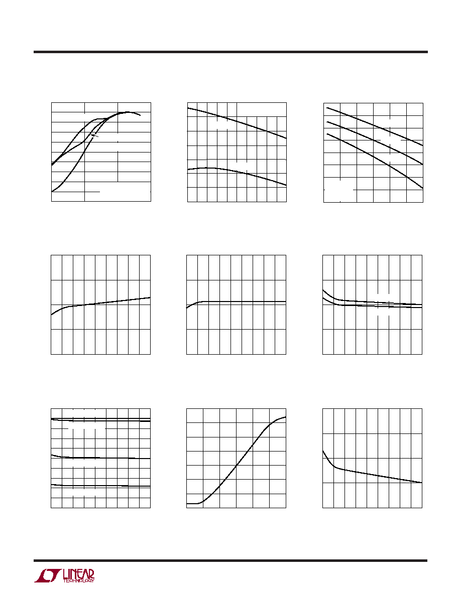
TYPICAL PERFOR A CE CHARACTERISTICS
U
W
Efficiency vs I
OUT
INDUCTOR CURRENT (A)
0.1
0
EFFICIENCY (%)
20
30
40
50
60
70
1
10
3738 G01
80
90
100
10
100
V
FCB/SYNC
= 5V
V
FCB/SYNC
= 0V
V
IN
= 12V
V
OUT
= 1.2V
FREQUENCY = 210kHz
V
FCB/SYNC
= OPEN
V
IN
(V)
4
85
EFFICIENCY (%)
86
88
89
90
92
5
9
11
3733 G02
87
91
8
13 14
6
7
10
12
I
L
= 20A
I
L
= 50A
V
IN
= 12V
FREQUENCY = 210kHz
FREQUENCY (kHz)
200
EFFICIENCY (%)
87
88
89
350
450
3738 G03
86
85
84
250
300
400
90
91
92
500
V
IN
= 5V
V
IN
= 10V
V
IN
= 14V
V
IN
= 12V
V
OUT
= 1.2V
I
LOAD
= 20A
Efficiency vs V
IN
Efficiency vs Frequency
Reference Voltage
vs Temperature
Error Amplifier g
m
vs Temperature
Maximum I
SENSE
Threshold
vs Temperature
TEMPERATURE (°C)
45
590
REFERENCE VOLTAGE (mV)
610
45
3738 G04
595
605
600
30
90
0
15
15
75
30
60
TEMPERATURE (°C)
45
2.0
ERROR AMPLIFIER g
m
(mmho)
4.0
45
3738 G05
2.5
3.5
3.0
30
90
0
15
15
75
30
60
TEMPERATURE (°C)
45
65
MAXIMUM I
SENSE
THRESHOLD (mV)
85
45
3738 G06
70
80
75
30
90
0
15
15
75
30
60
V
O
= 1.85V
V
O
= 0.8V
Oscillator Frequency
vs Temperature
Oscillator Frequency vs V
PLLFLTR
Undervoltage Reset Voltage
vs Temperature
TEMPERATURE (°C)
45
100
FREQUENCY (kHz)
600
550
500
450
400
350
300
45
3738 G07
150
250
200
30
90
0
15
15
75
30
60
V
PLLFLTR
= 2.4V
V
PLLFLTR
= 1.2V
V
PLLFLTR
= 0V
V
PLLFLTR
= 5V
V
PLLFLTR
(V)
0
200
FREQUENCY (kHz)
550
500
450
400
350
300
3738 G08
250
1.6
2.4
0.8
0.4
1.2
2.0
TEMPERATURE (°C)
45
3.0
UNDERVOLTAGE RESET (V)
5.0
45
3738 G09
3.5
4.5
4.0
30
90
0
15
15
75
30
60
T
A
= 25°C unless otherwise noted.