Äîêóìåíòàöèÿ è îïèñàíèÿ www.docs.chipfind.ru
LTC3802
1
3802f
s
Wide V
IN
Range: 3V to 30V Operation with Line
Feedforward Compensation
s
Leading Edge Modulation Architecture for
Extremely Low Duty Cycle Operation
s
Phase-Lockable Fixed Frequency: 330kHz to 750kHz
s
Two 180
°
Out-of-Phase Controllers
s
Fast Programmable Power-Up/-Down Tracking
s
Programmable Current Limit Without External
Current Sense Resistor
s
Optional Burst Mode
®
Operation at Light Load
s
±
1% 0.6V Voltage Reference
s
External N-Channel MOSFET Architecture
s
Low Shutdown Current: <100
µ
A
s
Overvoltage Protection and PGOOD Flag
s
Small 28-Lead SSOP and 32-Lead QFN Packages
Dual 550kHz Synchronous
2-Phase DC/DC Controller with
Programmable Up/Down Tracking
s
Notebook and Palmtop Computers
s
Portable Instruments
s
Battery-Operated Digital Devices
s
DC Power Distribution Systems
, LTC and LT are registered trademarks of Linear Technology Corporation.
Burst Mode is a registered trademark of Linear Technology Corporation.
U.S. Patent Nos 5481178, 5846544, 6304066, 6580258, 5055767, 6307356
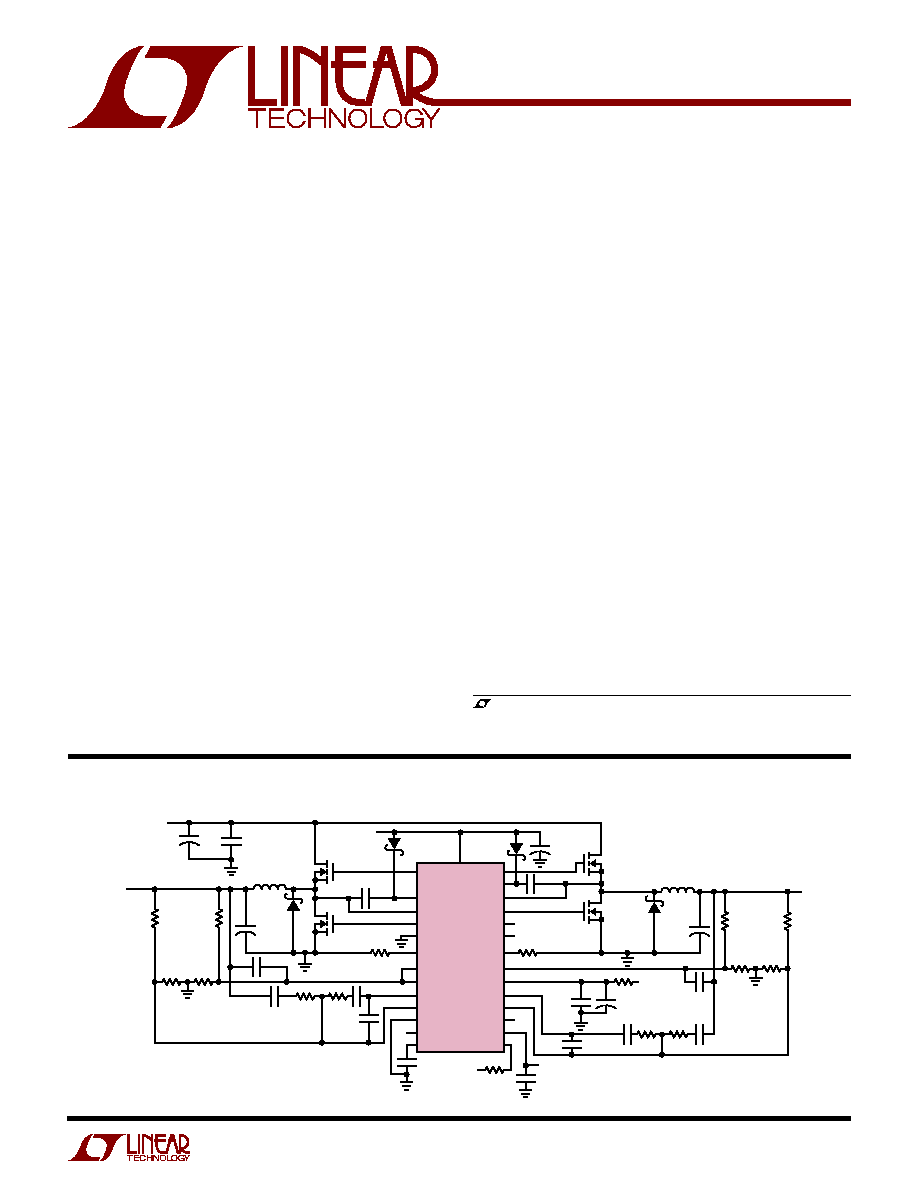
The LTC
®
3802 is a dual switching regulator controller
optimized for high efficiency step-down conversion from
input voltages between 3V to 30V. The controller uses a
leading edge modulation scheme to allow extremely low
duty cycle operation. The constant frequency voltage mode
controller allows a phase-lockable frequency between
330kHz and 750kHz. Power loss and noise due to the ESR
of the input capacitors are minimized by operating the two
controller output stages 180
°
out of phase. The synchro-
nous buck architecture automatically shifts to Burst Mode
operation as the output load decreases, ensuring maxi-
mum efficiency over a wide range of load currents.
The LTC3802 features an onboard, trimmed 0.6V refer-
ence and provides better than 1% regulation at the con-
verter outputs. A separate output sense provides real time
overvoltage protection and PGOOD sensing. An FBT pin
programs the power-up/-down tracking between the two
channels to meet various sequencing requirements. A
RUN/SS pin provides soft-start and externally program-
mable current limit protection functions.
DESCRIPTIO
U
FEATURES
APPLICATIO S
U
TYPICAL APPLICATIO
U
TG2
BOOST2
SW2
BG2
PLLIN
PLLLPF
I
MAX2
CMPIN2
V
CC
COMP2
FB2
PHASEMD
PGOOD
V
INFF
+
+
PV
CC
0.1
µ
F
0.1
µ
F
10
µ
F
CMDSH-3
Si7860DP
×
2
Si7860DP
×
2
4.7
µ
F
25V
×
8
Si7440DP
×
2
5V
CMDSH-3
2200pF
1500pF
560pF
330pF
15k
47k
47k
10k
5V
10
390
15k
5V
390
TG1
BOOST1
SW1
BG1
PGND
I
MAX1
FBT
CMPIN1
COMP1
FB1
SGND
FCB
RUN/SS
0.1
µ
F
B340B
B340B
1
µ
H
+
330
µ
F
4V
×
3
56
µ
F
25V
×
2
V
OUT1
3.3V
15A
V
IN
5V TO 22V
10k
10k
2.21k
2.21k
0.47
µ
F
V
IN
Si7440DP
×
2
1
µ
H
330
µ
F
4V
×
3
10k
10k
V
OUT2
2.5V
15A
3802 TA01
3.16k
3.16k
+
10
µ
F
330pF
560pF
1500pF
2200pF
0.1
µ
F
LTC3802
+
LTC3802
2
3802f
ABSOLUTE AXI U
RATI GS
W
W
W
U
(Note 1)
Consult LTC Marketing for parts specified with wider operating temperature ranges.
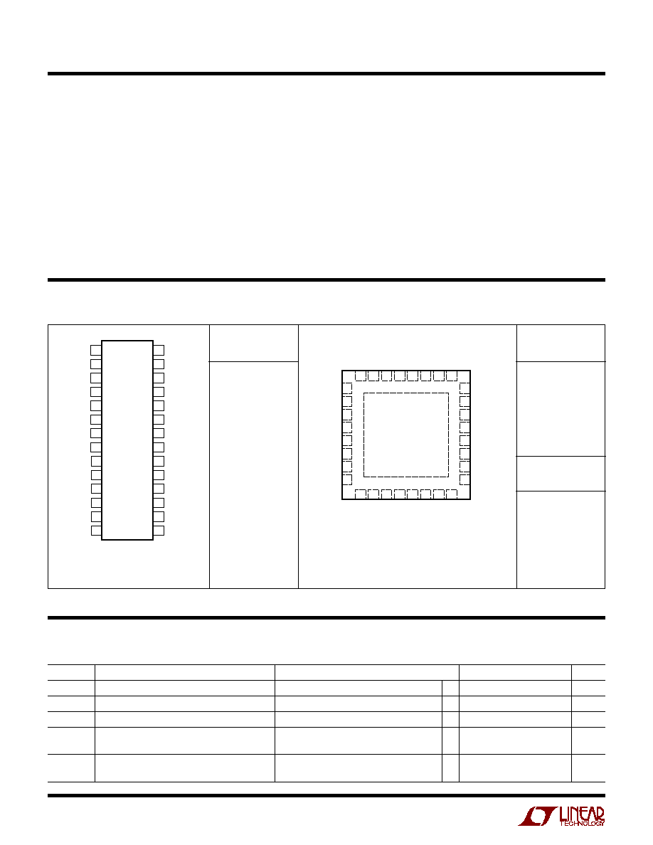
PACKAGE/ORDER I FOR ATIO
U
U
W
ORDER PART
NUMBER
LTC3802EGN
T
JMAX
= 125
°
C,
JA
= 110
°
C/W
T
JMAX
= 125
°
C,
JA
= 34
°
C/W
EXPOSED PAD (PIN 33) IS GND
MUST BE SOLDERED TO PCB
Supply Voltage
V
CC
, PV
CC
............................................................. 7V
BOOST
n .............................................................. 37V
BOOST
n SWn .................................................... 7V
SW
n ........................................................ 1V to 30V
Input Voltage
V
INFF
.................................................................... 30V
FB
n, CMPINn, FBT, PLLIN, FCB,
RUN/SS, PGOOD, PLLLPF, PHASEMD,
EXTREF, I
MAX
n .......................... 0.3V to V
CC
+ 0.3V
Extended Commercial
Operating Temperature Range (Note 2) .. 40
°
C to 85
°
C
Storage Temperature Range
LTC3802EGN ................................... 65
°
C to 150
°
C
LTC3802EUH ................................... 65
°
C to 125
°
C
Lead Temperature (Soldering, 10 sec)
LTC3802EGN Only ........................................... 300
°
C
1
2
3
4
5
6
7
8
9
10
11
12
13
14
TOP VIEW
GN PACKAGE
28-LEAD PLASTIC SSOP
28
27
26
25
24
23
22
21
20
19
18
17
16
15
PV
CC
BG1
BOOST1
TG1
SW1
PGND
I
MAX1
FBT
CMPIN1
COMP1
FB1
SGND
FCB
RUN/SS
BG2
BOOST2
TG2
SW2
PLLIN
PLLLPF
I
MAX2
CMPIN2
V
CC
COMP2
FB2
PHASEMD
V
INFF
PGOOD
UH PART
MARKING
LTC3802EUH
ORDER PART
NUMBER
3802
32 31 30 29 28 27 26 25
9
10 11 12
TOP VIEW
33
UH PACKAGE
32-LEAD (5mm
×
5mm) PLASTIC QFN
13 14 15 16
17
18
19
20
21
22
23
24
8
7
6
5
4
3
2
1
SW1
PGND
PGND
I
MAX1
FBT
CMPIN1
COMP1
FB1
PGND
PGND
PLLIN
PLLLPF
I
MAX2
CMPIN2
V
CC
COMP2
TG1
BOOST1
BG1
PV
CC
BG2
BOOST2
TG2
SW2
SGND
FCB
EXTREF
RUN/SS
PGOOD
V
INFF
PHASEMD
FB2
ELECTRICAL CHARACTERISTICS
The
q
denotes the specifications which apply over the full operating
temperature range. (Note 3) V
CC
= PV
CC
= BOOST = 5V, unless otherwise specified.
SYMBOL
PARAMETER
CONDITIONS
MIN
TYP
MAX
UNITS
V
CC
V
CC
Supply Voltage
q
3
5
6
V
PV
CC
PV
CC
Supply Voltage
(Note 4)
q
5
6
V
BV
CC
BOOST Pin Voltage
V
BOOST
V
SW
(Note 4)
q
5
6
V
V
UVLO
Positive Undervoltage Lockout
Measured at V
CC
2.2
2.5
2.8
V
Measured at V
INFF
2.2
2.5
2.8
V
I
VCC
V
CC
Supply Current
V
FB
= V
COMP
q
6.5
9
mA
V
RUN/SS
= 0V, PLLIN Floating
q
100
150
µ
A

LTC3802
3
3802f
ELECTRICAL CHARACTERISTICS
The
q
denotes the specifications which apply over the full operating
temperature range. (Note 3) V
CC
= PV
CC
= BOOST = 5V, unless otherwise specified.
SYMBOL
PARAMETER
CONDITIONS
MIN
TYP
MAX
UNITS
I
PVCC
PV
CC
Supply Current
V
FB
= V
CMPIN
= 0V, No Load
2
mA
V
RUN/SS
= 0V (Notes 5, 6)
1
10
µ
A
I
BOOST
BOOST Pin Current
V
FB
= V
CMPIN
= 0V, No Load
1
mA
V
RUN/SS
= 0V (Notes 5, 6)
1
10
µ
A
Switcher Control Loop
V
FB
Feedback Voltage
V
EXTREF
= 5V, 0
°
C
T
70
°
C
0.594
0.600
0.606
V
V
EXTREF
= 5V
q
0.591
0.600
0.609
V
V
FB
Feedback Voltage V
CC
Line Regulation
V
CC
= 4.5V to 6V
±
0.01
%/V
V
OUT
Output Voltage Load Regulation
(Note 7)
0.1
±
0.2
%
A
ERR
Error AMP DC Gain
No Load, V
EXTREF
= V
RUN/SS
= V
CC
q
70
80
dB
GBW
Error AMP Gain Bandwidth Product
f = 100kHz (Note 7)
10
MHz
I
COMP
Error AMP Output Sink/Source Current
V
RUN/SS
= V
CC
±
12
mA
I
FB
Voltage Feedback Input Current
V
FB
= 0V to 1V
q
±
1
µ
A
I
CMPIN
Comparators Input Current
V
CMPIN
= 0V to 1V
q
±
1
µ
A
I
FBT
FBT Input Current
V
FBT
= 0V to 1V
q
±
1
µ
A
I
EXTREF
EXTREF Input Current
V
EXTREF
= 0V to 5V
q
±
1
µ
A
V
EXTREF
External Reference Not to Affect V
FB
q
1
V
A
LFF
Drop in Duty Cycle/
V
INFF
V
VINFF
= 5V to 30V
2.3
%/V
R
VINFF
V
INFF
Input Resistance
1
M
V
PGOOD
Positive Power Good Threshold
With Respect to 0.6V
q
5
10
15
%
Negative Power Good Threshold
With Respect to 0.6V
q
5
10
15
%
V
OVP
Overvoltage Threshold
With Respect to V
FB
3
5
9
%
V
BURRS
(V
CMPIN
V
FB
) to Reset
15
mV
Burst Mode Operation
12
mV
V
SAW
SAW Before Line Compensation
1.2
V
I
IMAX
I
MAX
Source Current
V
IMAX
= 1V
9.0
10
11.0
µ
A
q
8.5
10
11.5
µ
A
I
LIM(TH)
I
LIM
Comparator Offset
q
15
0
15
mV
V
IMAX
/I
LIM
Threshold
5
V/V
Hard I
LIM
/I
LIM
Threshold
V
CMPIN
= 0V
1.5
V/V
I
SS
RUN/SS Source Current
V
CMPIN
= V
FBT
= 0.6V, V
PHASEMD
= V
CC
5
7
9
µ
A
RUN/SS Sink/Source Current Ratio
V
CMPIN
= V
FBT
= 0.6V, V
PHASEMD
= 0V
1.5
2
2.5
µ
A/
µ
A
RUN/SS Sink Current, I
LIM
V
CMPIN
= V
FBT
= 0.6V
100
µ
A
RUN/SS Sink Current, Hard I
LIM
V
CMPIN
= V
FBT
= 0V
q
1
mA
V
SHDN
RUN/SS Shutdown Threshold
RUN/SS
q
0.4
0.8
1.2
V
LOGIC and PGOOD
I
PHASEMD
PHASEMD Pull-Up Current
V
PHASEMD
= 0V
7
µ
A
PHASEMD Pull-Down Current
V
PHASEMD
= 5V
2
µ
A
V
IH
PLLIN, FCB High Level Input Voltage
q
2.4
V
V
IL
PLLIN, FCB Low Level Input Voltage
q
0.8
V
I
PGOOD
V
PGOOD
Leakage Current
Power Good
±
1
µ
A
V
OLPG
V
PGOOD
Output Low Voltage
I
PGOOD
= 1mA
q
0.1
0.3
V
t
PGOOD
V
PGOOD
Falling Edge Delay
(Note 8)
q
100
150
µ
s
V
PGOOD
Rising Edge Delay
(Note 8)
10
µ
s
LTC3802
4
3802f
Note 1: Absolute Maximum Ratings are those values beyond which the life
of a device may be impaired.
Note 2: The LTC3802 is guaranteed to meet performance specifications
from 0
°
C to 70
°
C. Specifications over the 40
°
C to 85
°
C operating
temperature range are assured by design, characterization and correlation
with statistical process controls.
Note 3: All currents into device pins are positive; all currents out of device
pins are negative. All voltages are referenced to ground unless otherwise
specified.
Note 4: To ensure proper operation, PV
CC
and BV
CC
(V
BOOST
V
SW
) must
be greater than V
GS(ON)
of the external MOSFETs.
Note 5: Supply current in normal operation is dominated by the current
needed to charge and discharge the external MOSFET gates. This current
will vary with supply voltage and the external MOSFETs used.
Note 6: Supply current in shutdown is dominated by external MOSFET
leakage and may be significantly higher than the quiescent current drawn
by the LTC3802, especially at elevated temperature.
Note 7: Guaranteed by design, not subject to test.
Note 8: Rise and fall times are measured using 10% and 90% levels. Delay
and nonoverlap times are measured using 50% levels.
Note 9: If V
CMPIN
is less than 90% of its nominal value, BG minimum
pulse width is limited to 400ns.
Note 10: The LTC3802 leading edge modulation architecture does not
have a minimum TG pulse width requirement. The TG minimum pulse
width is limited by the rise and fall times.
ELECTRICAL CHARACTERISTICS
The
q
denotes the specifications which apply over the full operating
temperature range. (Note 3) V
CC
= PV
CC
= BOOST = 5V, unless otherwise specified.
SYMBOL
PARAMETER
CONDITIONS
MIN
TYP
MAX
UNITS
Switcher Switching Characteristics
f
OSC
Oscillator Frequency
PLLIN Open or V
PLLIN
= 0V
490
550
610
kHz
V
PLLLPF
= 1.2V
550
kHz
V
PLLLPF
= 0V
250
330
400
kHz
V
PLLLPF
= 2.4V
650
750
850
kHz
R
PLLIN
PLLIN Pull-Down Current Source
5
µ
A
I
PLLLPF
Phase Detector Output Current
Sourcing Capability
f
PLLIN
> f
OSC
15
µ
A
Sinking Capability
f
PLLIN
< f
OSC
15
µ
A
Phase
TG1
vs PLLIN
PHASEMD Floats
0
Deg
TG1
vs PLLIN
V
PHASEMD
= 5V
90
Deg
TG2
vs PLLIN
PHASEMD Floats
180
Deg
TG2
vs PLLIN
V
PHASEMD
= 5V
270
Deg
V
PHASEMD
Shutdown Threshold
q
1.2
1.7
V
Floating
2.0
V
90
°
Phase Threshold
q
3.5
4.0
4.5
V
DC
MIN
Minimum TG Duty Cycle
V
PLLIN
= 0V
q
0
%
DC
MAX
Maximum TG Duty Cycle
V
PLLIN
= 0V, V
CMPIN
= 0.6V (Note 9)
q
86
89
92
%
t
ON(MIN)
TG Minimum Pulse Width
(Notes 7, 10)
50
ns
BG Minimum Pulse Width
V
CMPIN
= 0V (Note 9)
400
ns
t
NOV
Driver Nonoverlap
No Load
10
30
80
ns
R
DS(ON)
TG High R
DS(ON)
I
OUT
= 100mA (Note 7)
1.6
2.20
TG Low R
DS(ON)
1.3
1.80
BG High R
DS(ON)
1.8
2.50
BG Low R
DS(ON)
0.7
1.00
LTC3802
5
3802f
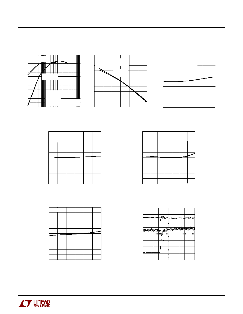
TYPICAL PERFOR A CE CHARACTERISTICS
U
W
Efficiency vs I
OUT
I
OUT
(A)
0.1
60
EFFICIENCY (%)
70
80
1
10
100
3802 G01
50
40
100
90
65
75
85
55
45
95
Burst Mode
OPERATION
CONTINUOUS
MODE
V
IN
= 12V
V
OUT
= 3.3V
T
A
= 25
°
C
CIRCUIT ON THE FIRST PAGE
OF THIS DATA SHEET
V
IN
(V)
0
80
EFFICIENCY (%)
84
88
92
5
10
15
20
3802 G02
25
96
100
82
86
90
94
98
30
T
A
= 25
°
C
CIRCUIT ON THE FIRST PAGE
OF THIS DATA SHEET
V
OUT
= 2.5V
I
OUT
= 5A
V
OUT
= 2.5V
I
OUT
= 10A
I
OUT
(A)
0
V
OUT
(V)
V
OUT
(%)
2.4975
2.5025
20
3802 G03
2.4925
2.4875
5
10
15
2.5125
2.5075
0.1
0.1
0.3
0.5
0.5
0.3
0.2
0
0.4
0.4
0.2
V
IN
= 12V
T
A
= 25
°
C
CIRCUIT ON THE FIRST PAGE
OF THIS DATA SHEET
Efficiency vs V
IN
Load Regulation
V
IN
(V)
0
V
OUT
(V)
V
OUT
(%)
2.5125
2.5075
2.5025
2.4975
2.4925
2.4875
0.5
0.3
0.1
0.1
0.3
0.4
0.2
0
0.2
0.4
0.5
5
10
15
20
3802 G04
25
30
V
CC
= 5V
I
OUT
= 5A
T
A
= 25
°
C
Line Regulation
TEMPERATURE (
°
C)
50
594.0
V
FB
(mV)
V
FB
(%)
595.2
597.6
598.8
600.0
606.0
602.4
0
50
75
LTC1323 · TPC05
596.4
603.6
604.8
601.2
1.0
0.8
0.4
0.2
0
1.0
0.4
0.6
0.6
0.8
0.2
25
25
100
125
V
CC
= 5V
V
CC
SUPPLY VOLTAGE (V)
3
597.0
V
FB
(mV)
V
FB
(%)
597.6
598.8
599.4
600.0
603.0
601.2
4
5
5.5
3802 G06
598.2
601.8
602.4
600.6
0.5
0.4
0.2
0.1
0
0.5
0.2
0.3
0.3
0.4
0.1
3.5
4.5
6
T
A
= 25
°
C
V
OUT
2.5V
(NO LOAD)
AC 50mV/DIV
V
IN
5V TO 15V
STEP
5V/DIV
C
IN
: 1
µ
F/50V
×
6
SANYO 35CV220AX
10
µ
s/DIV
3802 G07
V
COMP
AC 50mV/DIV
V
FB
vs Temperature
V
FB
vs V
CC
Supply Voltage
Line Feedforward Transient