Äîêóìåíòàöèÿ è îïèñàíèÿ www.docs.chipfind.ru
1
LTC3803-5
38035f
FEATURES
DESCRIPTIO
U
APPLICATIO S
U
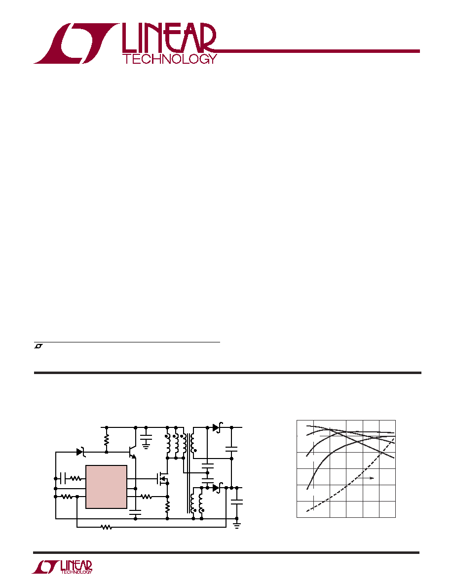
TYPICAL APPLICATIO
U
Constant Frequency
Current Mode Flyback
DC/DC Controller in ThinSOT
V
IN
and V
OUT
Limited Only by External Components
4.8V Undervoltage Lockout Threshold
Operating Junction Temperature from 40°C to
150°C
Adjustable Slope Compensation
Internal Soft-Start
Constant Frequency 200kHz Operation
±1.5% Reference Accuracy
Current Mode Operation for Excellent Line and Load
Transient Response
No Minimum Load Requirement
Low Quiescent Current: 240µA
Low Profile (1mm) SOT-23 Package
42V and 12V Automotive Power Supplies
Telecom Power Supplies
Auxiliary/Housekeeping Power Supplies
Power Over Ethernet
ThinSOT is a trademark of Linear Technology Corporation.
Dual Output Wide Input Range Converter
The LTC
®
3803-5 is a constant frequency current mode
flyback controller optimized for driving 4.5V and 6V-rated
N-channel MOSFETs in high input voltage applications.
The LTC3803-5 operates from inputs as low as 5V. Con-
stant frequency operation is maintained down to very light
loads, resulting in less low frequency noise generation
over a wide range of load currents. Slope compensation
can be programmed with an external resistor.
The LTC3803-5 provides ±1.5% output voltage accuracy
and consumes only 240µA of quiescent current. Ground-
referenced current sensing allows LTC3803-5-based con-
verters to accept input supplies beyond the LTC3803-5's
absolute maximum V
CC
. For simplicity, the LTC3803-5
can be powered from a high V
IN
through a resistor, due to
its internal 8V shunt regulator. An internal undervoltage
lockout shuts down the IC when the input voltage falls
below 3.2V, guaranteeing at least 3.2V of gate drive to the
external MOSFET.
The LTC3803-5 is available in a low profile (1mm) 6-lead
SOT-23 (ThinSOT
TM
) package.
Efficiency and Power Loss
vs Output Power
, LTC and LT are registered trademarks of Linear Technology Corporation.
All other trademarks are the property of their respective owners.
I
TH
/RUN
GND
V
FB
LTC3803-5
NGATE
V
CC
SENSE
10MQ100N
B3100
1µF
100V
3x
13V/0.3A
20mA MIN
LOAD
6.5V/1.2A
38035 TA01
0.012
0.1µF
22k
7.5k
57.6k
8.06k
4.7k
10nF
1µF
100V
1µF
100V
PHM25NQ10T
ALL CAPACITORS ARE X7R, TDK
V
IN
6V TO 50V
MMBTA42
22µF
10V
47µF
10V
PDZ9.1B
VPH5-0155
OUTPUT POWER (W)
0
2
EFFICIENCY (%)
POWER LOSS (W)
90
85
80
75
70
65
60
3.0
2.5
2.0
1.5
1.0
0.5
0
4
6
8
10
38035 TA01b
12
V
IN
= 8V
V
IN
= 12V
V
IN
= 12V
V
IN
= 24V
V
IN
= 48V
2
LTC3803-5
38035f
ORDER PART
NUMBER
(Note 1)
V
CC
to GND (Current Fed) .................... 25mA into V
CC
*
NGATE Voltage ......................................... 0.3V to V
CC
V
FB
, I
TH
/RUN Voltages .............................. 0.3V to 3.5V
SENSE Voltage ........................................... 0.3V to 1V
NGATE Peak Output Current (<10µs) ........................ 1A
Operating Junction Temperature Range (Note 2)
LTC3803E-5 ....................................... 40°C to 85°C
LTC3803H-5 (Note 3) ....................... 40°C to 150°C
Storage Temperature Range ................. 65°C to 150°C
Lead Temperature (Soldering, 10 sec).................. 300°C
LTC3803HS6-5
LTC3803ES6-5
T
JMAX
= 150°C,
JA
= 165°C/W
ABSOLUTE
M
AXI
M
U
M
RATINGS
W
W
W
U
PACKAGE/ORDER I
N
FOR
M
ATIO
N
W
U
U
SYMBOL
PARAMETER
CONDITIONS
MIN
TYP
MAX
UNITS
V
TURNON
V
CC
Turn On Voltage
4
4.8
5.7
V
V
TURNOFF
V
CC
Turn Off Voltage
3.3
4
4.9
V
V
HYST
V
CC
Hysteresis
V
TURNON
V
TURNOFF
0.05
0.8
V
V
CLAMP1mA
V
CC
Shunt Regulator Voltage
I
CC
= 1mA, V
ITH/RUN
= 0V
6.2
8
9.9
V
V
CLAMP25mA
V
CC
Shunt Regulator Voltage
I
CC
= 25mA, V
ITH/RUN
= 0V
6.3
8.1
10.3
V
I
CC
Input DC Supply Current
(Note 4)
Normal Operation
V
ITH/RUN
= 1.3V
240
350
µA
Undervoltage
V
CC
= V
TURNON
100mV
40
90
µA
V
ITHSHDN
Shutdown Threshold (at I
TH
/RUN)
V
CC
= V
TURNON
+ 100mV
0.12
0.28
0.45
V
I
ITHSTART
Start-Up Current Source
V
ITH/RUN
= 0V
0.07
0.34
0.8
µA
V
FB
Regulated Feedback Voltage
0°C T
J
85°C (Note 5)
0.788
0.800
0.812
V
40°C T
J
85°C (Note 5)
0.780
0.800
0.816
V
g
m
Error Amplifier Transconductance
I
TH/RUN
Pin Load = ±5µA (Note 5)
200
333
500
µA/V
V
O(LINE)
Output Voltage Line Regulation
V
TURNOFF
< V
CC
< V
CLAMP
(Note 5)
0.1
mV/V
V
O(LOAD)
Output Voltage Load Regulation
I
TH
/RUN Sinking 5µA (Note 5)
3
mV/µA
I
TH
/RUN Sourcing 5µA (Note 5)
3
mV/µA
I
FB
V
FB
Input Current
(Note 5)
10
50
nA
f
OSC
Oscillator Frequency
V
ITH/RUN
= 1.3V
170
200
230
kHz
DC
ON(MIN)
Minimum Switch On Duty Cycle
V
ITH/RUN
= 1.3V, V
FB
= 0.8V
6.5
8.5
%
DC
ON(MAX)
Maximum Switch On Duty Cycle
V
ITH/RUN
= 1.3V, V
FB
= 0.8V
70
80
90
%
t
RISE
Gate Drive Rise Time
C
LOAD
= 3000pF
40
ns
t
FALL
Gate Drive Fall Time
C
LOAD
= 3000pF
40
ns
V
IMAX
Peak Current Sense Voltage
R
SL
= 0 (Note 6)
90
100
115
mV
I
SLMAX
Peak Slope Compensation Output Current
(Note 7)
5
µA
t
SFST
Soft-Start Time
0.7
ms
LTC3803E-5: The
indicates specifications which apply over the full 40°C
to 85°C operating junction temperature range, otherwise specifications are at T
J
= 25°C. V
CC
= 5V, unless otherwise noted. (Note 2)
LTBMH
LTBPF
Consult LTC Marketing for parts specified with wider operating temperature ranges.
ELECTRICAL CHARACTERISTICS
I
TH
/RUN 1
GND 2
V
FB
3
6 NGATE
5 V
CC
4 SENSE
TOP VIEW
S6 PACKAGE
6-LEAD PLASTIC TSOT-23
*LTC3803-5 internal clamp circuit self regulates V
CC
voltage to 8V.
S6 PART
MARKING
3
LTC3803-5
38035f
SYMBOL
PARAMETER
CONDITIONS
MIN
TYP
MAX
UNITS
V
TURNON
V
CC
Turn On Voltage
3.9
4.8
5.7
V
V
TURNOFF
V
CC
Turn Off Voltage
3.2
4
4.9
V
V
HYST
V
CC
Hysteresis
V
TURNON
V
TURNOFF
0.05
0.8
V
V
CLAMP1mA
V
CC
Shunt Regulator Voltage
I
CC
= 1mA, V
ITH/RUN
= 0V
6.2
8
10.4
V
V
CLAMP25mA
V
CC
Shunt Regulator Voltage
I
CC
= 25mA, V
ITH/RUN
= 0V
6.3
8.1
10.7
V
I
CC
Input DC Supply Current
(Note 4)
Normal Operation
V
ITH/RUN
= 1.3V
240
350
µA
Undervoltage
V
CC
= V
TURNON
100mV
40
100
µA
V
ITHSHDN
Shutdown Threshold (at I
TH
/RUN)
V
CC
= V
TURNON
+ 100mV
0.08
0.28
0.45
V
I
ITHSTART
Start-Up Current Source
V
ITH/RUN
= 0V
0.07
0.34
1
µA
V
FB
Regulated Feedback Voltage
0°C T
J
85°C (Note 5)
0.788
0.800
0.812
V
40°C T
J
150°C (Note 5)
0.780
0.800
0.820
V
g
m
Error Amplifier Transconductance
I
TH/RUN
Pin Load = ±5µA (Note 5)
200
333
500
µA/V
V
O(LINE)
Output Voltage Line Regulation
V
TURNOFF
< V
CC
< V
CLAMP
(Note 5)
0.1
mV/V
V
O(LOAD)
Output Voltage Load Regulation
I
TH
/RUN Sinking 5µA (Note 5)
3
mV/µA
I
TH
/RUN Sourcing 5µA (Note 5)
3
mV/µA
I
FB
V
FB
Input Current
(Note 5)
10
50
nA
f
OSC
Oscillator Frequency
V
ITH/RUN
= 1.3V
170
200
230
kHz
DC
ON(MIN)
Minimum Switch On Duty Cycle
V
ITH/RUN
= 1.3V, V
FB
= 0.8V
6.5
8.5
%
DC
ON(MAX)
Maximum Switch On Duty Cycle
V
ITH/RUN
= 1.3V, V
FB
= 0.8V
70
80
90
%
t
RISE
Gate Drive Rise Time
C
LOAD
= 3000pF
40
ns
t
FALL
Gate Drive Fall Time
C
LOAD
= 3000pF
40
ns
V
IMAX
Peak Current Sense Voltage
R
SL
= 0 (Note 6)
85
100
115
mV
I
SLMAX
Peak Slope Compensation Output Current
(Note 7)
5
µA
t
SFST
Soft-Start Time
0.7
ms
LTC3803H-5: The
indicates specifications which apply over the full 40°C
to 150°C operating junction temperature range, otherwise specifications are at T
A
= 25°C. V
CC
= 5V, unless otherwise noted.
(Notes 2, 3)
Note 1: Absolute Maximum Ratings are those values beyond which the life
of a device may be impaired.
Note 2: The LTC3803H-5 is guaranteed to meet specifications from 40°C
to 150°C. The LTC3803E-5 is guaranteed to meet specifications from 0°C
to 85°C with specifications over the 40°C to 85°C temperature range
assured by design, characterization and correlation with statistical process
controls.
Junction temperature (T
J)
is calculated from the ambient temperature T
A
and the power dissipation P
D
in the LTC3803-5 using the formula:
T
J
= T
A
+ (P
D
· 230°C/W)
Note 3: High junction temperatures degrade operating lifetimes. Operating
ELECTRICAL CHARACTERISTICS
lifetime at junction temperatures greater than 125°C is derated to 1000
hours.
Note 4: Dynamic supply current is higher due to the gate charge being
delivered at the switching frequency.
Note 5: The LTC3803-5 is tested in a feedback loop that servos V
FB
to the
output of the error amplifier while maintaining I
TH
/RUN at the midpoint of
the current limit range.
Note 6: Peak current sense voltage is reduced dependent on duty cycle
and an optional external resistor in series with the SENSE pin (R
SL
). For
details, refer to the programmable slope compensation feature in the
Applications Information section.
Note 7: Guaranteed by design.
4
LTC3803-5
38035f
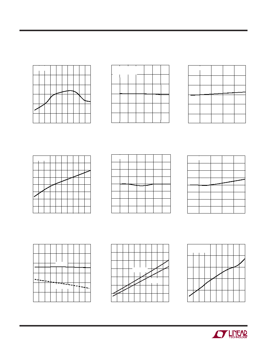
TYPICAL PERFOR A CE CHARACTERISTICS
U
W
Reference Voltage
vs V
CC
Shunt Regulator Current
Reference Voltage
vs Supply Voltage
Reference Voltage vs Temperature
Oscillator Frequency
vs V
CC
Shunt Regulator Current
Oscillator Frequency
vs Supply Voltage
Oscillator Frequency
vs Temperature
I
CC
Supply Current
vs Temperature
V
CC
Shunt Regulator Voltage
vs Temperature
V
CC
Undervoltage Lockout
Thresholds vs Temperature
TEMPERATURE (°C)
50
V
FB
VOLTAGE (mV)
70 90
38035 G01
10 10
30
30 50
150
110 130
812
808
804
800
796
792
788
V
CC
= 5V
V
CC
SUPPLY VOLTAGE (V)
4.0
V
FB
VOLTAGE (mV)
792
796
812
800
5.0
6.0
6.5
38035 F02
788
804
808
4.5
5.5
7.0
7.5
T
A
= 25°C
V
CC
V
CLAMP1mA
I
CC
(mA)
0
V
FB
VOLTAGE (mV)
792
796
800
15
25
38035 G03
788
5
10
20
804
808
812
T
A
= 25°C
TEMPERATURE (°C)
50
OSCILLATOR FREQUENCY (kHz)
10
30
70
150
110 130
38035 G04
30
10
50
90
V
CC
= 5V
220
215
210
205
200
195
190
185
180
V
CC
SUPPLY VOLTAGE (V)
4.0
OSCILLATOR FREQUENCY (kHz)
180
190
200
4.5
5.0
5.5
6.0
38035 G05
6.5
7.0
210
220
185
195
205
215
7.5
T
A
= 25°C
I
CC
(mA)
0
OSCILLATOR FREQUENCY (kHz)
180
190
200
5
10
15
20
38035 G06
210
220
185
195
205
215
25
T
A
= 25°C
TEMPERATURE (°C)
50
5.0
VOLTS
5.5
4.5
3.5
6.0
10
30
50
3803 G07
3.0
4.0
30
10
70 90
150
110 130
V
TURNON
V
TURNOFF
TEMPERATURE (°C)
50
V
CC
(V)
7.0
7.5
8.0
10.5
9.0
10
30 50
38035 G08
9.5
10.0
8.5
30
10
70 90
150
130
110
I
CC
= 25mA
I
CC
= 1mA
TEMPERATURE (°C)
50
SUPPLY CURRENT (
µ
A)
200
300
240
10
30 50
38035 G08
260
280
220
30
10
70 90 110 130 150
V
CC
= 5V
V
ITH/RUN
= 1.3V

5
LTC3803-5
38035f
TYPICAL PERFOR A CE CHARACTERISTICS
U
W
I
TH
/RUN Shutdown Threshold
vs Temperature
Start-Up I
CC
Supply Current
vs Temperature
I
TH
/RUN Start-Up Current Source
vs Temperature
Soft-Start Time vs Temperature
Peak Current Sense Voltage
vs Temperature
TEMPERATURE (°C)
50
0
START-UP SUPPLY CURRENT (
µ
A)
10
20
30
40
10
30
70
110 130 150
38035 G10
50
60
70
30
10
50
90
V
CC
= V
TURNON
0.1V
TEMPERATURE (°C)
50
SHUTDOWN THRESHOLD (mV)
300
350
400
70
90
250
200
10 10
30
30
50
150
110 130
150
100
50
0
450
500
3803 G11
TEMPERATURE (°C)
50
0
I
TH
/RUN PIN CURRENT SOURCE (nA)
100
200
300
400
10
30
70
110 130 150
38035 G12
500
600
700
800
900
1000
30
10
50
90
V
CC
= V
TURNON
+ 0.1V
V
ITH/RUN
= 0V
TEMPERATURE (°C)
50
SENSE PIN VOLTAGE (mV)
100
110
150
110 130
38035 G13
90
80
10
30
70
30
10
50
90
120
95
105
85
115
V
CC
= 5V
TEMPERATURE (°C)
50
SOFT-START TIME (ms)
0.6
1.0
150
38035 G14
0.2
0
10
30
70
30
10
50
130
110
90
1.4
0.4
0.8
1.2
V
CC
= 5V