Äîêóìåíòàöèÿ è îïèñàíèÿ www.docs.chipfind.ru
1
LTC3830/LTC3830-1
sn3830 3830fs
High Power Step-Down
Synchronous DC/DC Controllers
for Low Voltage Operation
s
High Power Switching Regulator Controller
for 3.3V-5V to 1.xV-3.xV Step-Down Applications
s
No Current Sense Resistor Required
s
Low Input Supply Voltage Range: 3V to 8V
s
Maximum Duty Cycle > 91% Over Temperature
s
All N-Channel External MOSFETs
s
Excellent Output Regulation:
±
1% Over Line, Load
and Temperature Variations
s
High Efficiency: Over 95% Possible
s
Adjustable or Fixed 3.3V Output (16-Pin Version)
s
Programmable Fixed Frequency Operation: 100kHz to
500kHz
s
External Clock Synchronization
s
Soft-Start (Some Versions)
s
Low Shutdown Current: <10
µ
A
s
Overtemperature Protection
s
Available in S8, S16 and SSOP-16 Packages
s
CPU Power Supplies
s
Multiple Logic Supply Generator
s
Distributed Power Applications
s
High Efficiency Power Conversion
The LTC
®
3830/LTC3830-1 are high power, high effi-
ciency switching regulator controllers optimized for
3.3V-5V to 1.xV-3.xV step-down applications. A preci-
sion internal reference and feedback system provide
±
1% output regulation over temperature, load current
and line voltage variations. The LTC3830/LTC3830-1 use
a synchronous switching architecture with N-channel
MOSFETs. Additionally, the chip senses output current
through the drain-source resistance of the upper
N-channel FET, providing an adjustable current limit
without a current sense resistor.
The LTC3830/LTC3830-1 operate with an input supply
voltage as low as 3V and with a maximum duty cycle of
>91% over temperature. They include a fixed frequency
PWM oscillator for low output ripple operation. The 200kHz
free-running clock frequency can be externally adjusted or
synchronized with an external signal from 100kHz to 500kHz.
In shutdown mode, the LTC3830 supply current drops to
<10
µ
A. The LTC3830-1 differs from the LTC3830 S8 ver-
sion by replacing shutdown with a soft-start function.
For a similar, pin compatible DC/DC converter with an
output voltage as low as 0.6V, please refer to the LTC3832.
, LTC and LT are registered trademarks of Linear Technology Corporation.
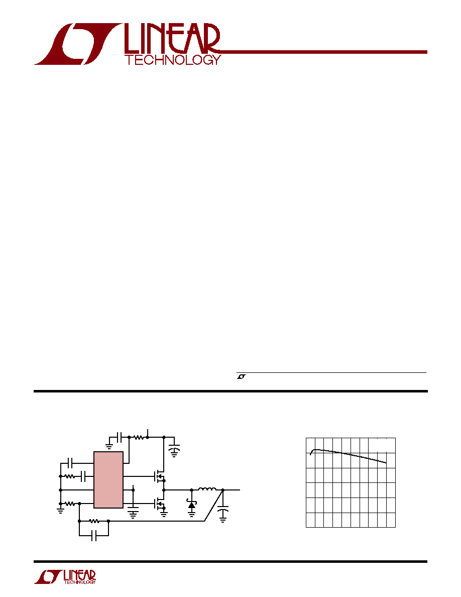
Figure 1. High Efficiency 3V-8V to 1.8V Power Converter
+
+
0.01
µ
F
15k
SS
COMP
GND
FB
PV
CC2
G1
PV
CC1
G2
LTC3830-1
12V
3.3nF
0.1
µ
F
4.7
µ
F
M1
Si7806DN
4.7
µ
F
B320A
220
µ
F
10V
1.8V
9A
L
3.2
µ
H
M2
Si7806DN
L: SUMIDA CDEP105-3R2MC-88
C
OUT
: PANASONIC EEFUEOD271R
C
OUT
270
µ
F
2V
3830 F01
5.1
V
IN
3V TO 8V
12.7k 1%
5.36k 1%
LOAD CURRENT (A)
40
EFFICIENCY (%)
60
80
100
50
70
90
2
4
6
8
3830 TA02
10
1
0
3
5
7
9
V
IN
= 3.3V
V
OUT
= 1.8V
Efficiency
DESCRIPTIO
U
FEATURES
APPLICATIO S
U
TYPICAL APPLICATIO
U
2
LTC3830/LTC3830-1
sn3830 3830fs
Supply Voltage
V
CC
....................................................................... 9V
PV
CC1,2
................................................................ 14V
Input Voltage
I
FB
, I
MAX
............................................... 0.3V to 14V
SENSE
+
, SENSE
, FB,
SHDN, FREQSET ....................... 0.3V to V
CC
+ 0.3V
ORDER PART
NUMBER
LTC3830ES8
T
JMAX
= 125
°
C,
JA
= 130
°
C/ W
ABSOLUTE AXI U RATI GS
W
W
W
U
PACKAGE/ORDER I FOR ATIO
U
U
W
S8
PART MARKING
3830
(Note 1)
Junction Temperature ........................................... 125
°
C
Operating Temperature Range (Note 9) .. 40
°
C to 85
°
C
Storage Temperature Range ................. 65
°
C to 150
°
C
Lead Temperature (Soldering, 10 sec).................. 300
°
C
1
2
3
4
8
7
6
5
TOP VIEW
G2
V
CC
/PV
CC2
COMP
SHDN
G1
PV
CC1
GND
FB
S8 PACKAGE
8-LEAD PLASTIC SO
ORDER PART
NUMBER
LTC3830-1ES8
S8
PART MARKING
38301
1
2
3
4
8
7
6
5
TOP VIEW
G2
V
CC
/PV
CC2
COMP
SS
G1
PV
CC1
GND
FB
S8 PACKAGE
8-LEAD PLASTIC SO
T
JMAX
= 125
°
C,
JA
= 130
°
C/ W
ORDER PART
NUMBER
LTC3830EGN
LTC3830ES
T
JMAX
= 125
°
C,
JA
= 130
°
C/ W (GN)
T
JMAX
= 125
°
C,
JA
= 100
°
C/ W (S)
GN PACKAGE
16-LEAD PLASTIC SSOP
S PACKAGE
16-LEAD PLASTIC SO
1
2
3
4
5
6
7
8
TOP VIEW
16
15
14
13
12
11
10
9
G1
PV
CC1
PGND
GND
SENSE
FB
SENSE
+
SHDN
G2
PV
CC2
V
CC
I
FB
I
MAX
FREQSET
COMP
SS
Consult LTC Marketing for parts specified with wider operating temperature ranges.
SYMBOL
PARAMETER
CONDITIONS
MIN
TYP
MAX
UNITS
V
CC
Supply Voltage
q
3
5
8
V
PV
CC
PV
CC1
, PV
CC2
Voltage
(Note 7)
q
3
13.2
V
V
UVLO
Undervoltage Lockout Voltage
2.4
2.9
V
V
FB
Feedback Voltage
V
COMP
= 1.25V
1.255
1.265
1.275
V
q
1.252
1.265
1.278
V
V
OUT
Output Voltage
V
COMP
= 1.25V
3.250
3.3
3.350
V
q
3.235
3.3
3.365
V
V
OUT
Output Load Regulation
I
OUT
= 0A to 10A (Note 6)
2
mV
Output Line Regulation
V
CC
= 4.75V to 5.25V
0.1
mV
The
q
denotes specifications that apply over the full operating temperature
range, otherwise specifications are at T
A
= 25
°
C. V
CC
, PV
CC1
, PV
CC2
= 5V, unless otherwise noted. (Note 2)
ELECTRICAL CHARACTERISTICS
GN PART
MARKING
3830
3
LTC3830/LTC3830-1
sn3830 3830fs
SYMBOL
PARAMETER
CONDITIONS
MIN
TYP
MAX
UNITS
I
VCC
Supply Current
Figure 2, V
SHDN
= V
CC
q
0.7
1.6
mA
V
SHDN
= 0V
q
1
10
µ
A
I
PVCC
PV
CC
Supply Current
Figure 2, V
SHDN
= V
CC
(Note 3)
q
14
20
mA
V
SHDN
= 0V
q
0.1
10
µ
A
f
OSC
Internal Oscillator Frequency
FREQSET Floating
q
160
200
250
kHz
V
SAWL
V
COMP
at Minimum Duty Cycle
1.2
V
V
SAWH
V
COMP
at Maximum Duty Cycle
2.2
V
V
COMPMAX
Maximum V
COMP
V
FB
= 0V, PV
CC1
= 8V
2.85
V
f
OSC
/
I
FREQSET
Frequency Adjustment
10
kHz/
µ
A
A
V
Error Amplifier Open-Loop DC Gain
Measured from FB to COMP,
q
46
55
dB
SENSE
+
and SENSE
Floating, (Note 4)
g
m
Error Amplifier Transconductance
Measured from FB to COMP,
q
520
650
780
µ
mho
SENSE
+
and SENSE
Floating, (Note 4)
I
COMP
Error Amplifier Output Sink/Source Current
100
µ
A
I
MAX
I
MAX
Sink Current
V
IMAX
= V
CC
9
12
15
µ
A
(Note 10)
q
4
12
20
µ
A
I
MAX
Sink Current Tempco
V
IMAX
= V
CC
(Note 6)
3300
ppm/
°
C
V
IH
SHDN Input High Voltage
q
2.4
V
V
IL
SHDN Input Low Voltage
q
0.8
V
I
IN
SHDN Input Current
V
SHDN
= V
CC
q
0.1
1
µ
A
I
SS
Soft-Start Source Current
V
SS
= 0V, V
IMAX
= 0V, V
IFB
= V
CC
q
8
12
16
µ
A
I
SSIL
Maximum Soft-Start Sink Current
V
IMAX
= V
CC
, V
IFB
= 0V,
1.6
mA
In Current Limit
V
SS
= V
CC
(Note 8), PV
CC1
= 8V
R
SENSE
SENSE Input Resistance
29.2
k
R
SENSEFB
SENSE to FB Resistance
18
k
t
r
, t
f
Driver Rise/Fall Time
Figure 2, PV
CC1
= PV
CC2
= 5V (Note 5)
q
80
250
ns
t
NOV
Driver Nonoverlap Time
Figure 2, PV
CC1
= PV
CC2
= 5V (Note 5)
q
25
120
250
ns
DC
MAX
Maximum G1 Duty Cycle
Figure 2, V
FB
= 0V (Note 5), PV
CC1
= 8V
q
91
95
%
The
q
denotes specifications that apply over the full operating temperature
range, otherwise specifications are at T
A
= 25
°
C. V
CC
, PV
CC1
, PV
CC2
= 5V, unless otherwise noted. (Note 2)
ELECTRICAL CHARACTERISTICS
Note 1: Absolute Maximum Ratings are those values beyond which the life
of a device may be impaired.
Note 2: All currents into device pins are positive; all currents out of device
pins are negative. All voltages are referenced to ground unless otherwise
specified.
Note 3: Supply current in normal operation is dominated by the current
needed to charge and discharge the external FET gates. This will vary with
the LTC3830 operating frequency, operating voltage and the external FETs
used.
Note 4: The open-loop DC gain and transconductance from the SENSE
+
and SENSE
pins to COMP pin will be (A
V
)(1.265/3.3) and (g
m
)(1.265/3.3)
respectively.
Note 5: Rise and fall times are measured using 10% and 90% levels. Duty
cycle and nonoverlap times are measured using 50% levels.
Note 6: Guaranteed by design, not subject to test.
Note 7: PV
CC1
must be higher than V
CC
by at least 2.5V for the current
limit protection circuit to be active.
Note 8: The current limiting amplifier can sink but cannot source current.
Under normal (not current limited) operation, the output current will be
zero.
Note 9: The LTC3830E/LTC3830-1E are guaranteed to meet performance
specifications from 0
°
C to 70
°
C. Specifications over the 40
°
C to 85
°
C
operating temperature range are assured by design, characterization and
correlation with statistical process controls.
Note 10: The minimum and maximum limits for I
MAX
over temperature
includes the intentional temperature coefficient of 3300ppm/
°
C. This
induced temperature coefficient counteracts the typical temperature
coefficient of the external power MOSFET on-resistance. This results in a
relatively flat current limit over temperature for the application.
4
LTC3830/LTC3830-1
sn3830 3830fs
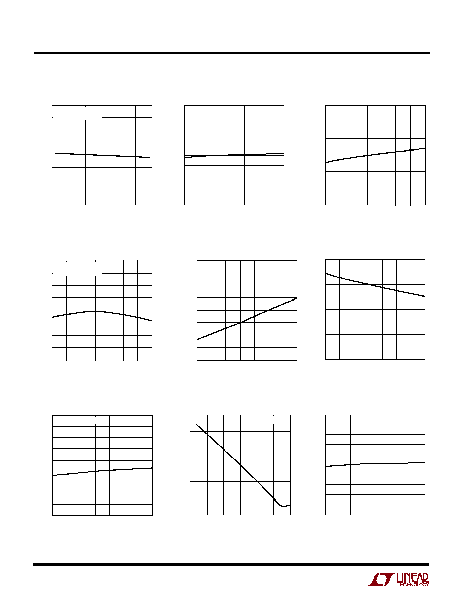
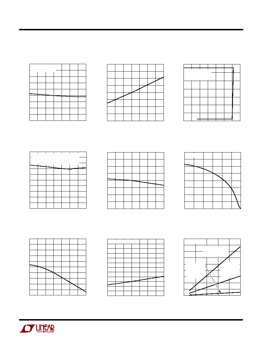
TYPICAL PERFOR A CE CHARACTERISTICS
U
W
Load Regulation
OUTPUT CURRENT (A)
15
V
OUT
(V)
3.33
0
3830 G02
3.30
3.28
10
5
5
3.27
3.26
3.34
3.32
3.31
3.29
10
15
T
A
= 25
°
C
REFER TO FIGURE 12
Line Regulation
SUPPLY VOLTAGE (V)
3
V
FB
(V)
V
FB
(mV)
1.267
1.271
1.275
7
3830 G03
1.263
1.259
1.265
1.269
1.273
1.261
1.257
1.255
2
6
10
2
6
0
4
8
4
8
10
4
5
6
8
T
A
= 25
°
C
Output Voltage Temperature Drift
TEMPERATURE (
°
C)
50
V
OUT
(V)
V
OUT
(mV)
3.33
25
3830 G04
3.30
3.28
25
0
50
3.27
3.26
3.34
3.32
3.31
3.29
30
0
20
30
40
40
20
10
10
75
100
125
REFER TO FIGURE 12
OUTPUT = NO LOAD
Error Amplifier Transconductance
vs Temperature
TEMPERATURE (°C)
50
ERROR AMPLIFIER TRANSCONDUCTANCE (
µ
mho)
700
750
800
25
75
3830 G05
650
600
25
0
50
100
125
550
500
TEMPERATURE (
°
C)
50
ERROR AMPLIFIER SINK/SOURCE CURRENT (
µ
A)
180
25
3830 G06
120
80
25
0
50
60
40
200
160
140
100
75
100
125
TEMPERATURE (
°
C)
50
40
ERROR AMPLIFIER OPEN-LOOP GAIN (dB)
45
50
55
60
25
0
25
50
2830 G07
75
100
125
Error Amplifier Sink/Source
Current vs Temperature
Error Amplifier Open-Loop Gain
vs Temperature
Oscillator Frequency
vs Temperature
Oscillator Frequency
vs FREQSET Input Current
Oscillator (V
SAWH
V
SAWL
)
vs External Sync Frequency
TEMPERATURE (
°
C)
50
160
OSCILLATOR FREQUENCY (kHz)
170
190
200
210
50
250
3831 G08
180
0
25
75
100
25
125
220
230
240
FREQSET FLOATING
FREQSET INPUT CURRENT (
µ
A)
40
0
OSCILLATOR FREQUENCY (kHz) 100
200
300
400
600
30
20
10
0
3830 G09
10
20
500
T
A
= 25
°
C
EXTERNAL SYNC FREQUENCY (kHz)
100
0.5
V
SAWH
V
SAWL
(V)
0.6
0.8
0.9
1.0
1.5
1.2
200
300
3830 G10
0.7
1.3
1.4
1.1
400
500
T
A
= 25
°
C
5
LTC3830/LTC3830-1
sn3830 3830fs
TYPICAL PERFOR A CE CHARACTERISTICS
U
W
Maximum G1 Duty Cycle
vs Temperature
I
MAX
Sink Current
vs Temperature
Output Overcurrent Protection
Output Current Limit Threshold
vs Temperature
Soft-Start Source Current
vs Temperature
Soft-Start Sink Current
vs (V
IFB
V
IMAX
)
TEMPERATURE (
°
C)
50
91
MAXIMUM G1 DUTY CYCLE (%)
92
94
95
96
50
100
3830 G11
93
0
25
75
100
25
125
97
98
99
V
FB
= 0V
REFER TO FIGURE 3
TEMPERATURE (
°
C)
50
I
MAX
SINK CURRENT (
µ
A)
18
25
3830 G12
12
8
25
0
50
6
4
20
16
14
10
75
100
125
OUTPUT CURRENT (A)
0
3.5
3.0
2.5
2.0
1.5
1.0
0.5
0
3830 G13
2
4
6
8
10
12
14
OUTPUT VOLTAGE (V)
T
A
= 25
°
C
REFER TO FIGURE 12
R
IMAX
= 20k
TEMPERATURE (
°
C)
50
5
OUTPUT CURRENT LIMIT (A)
6
8
9
10
15
12
0
50
75
3830 G14
7
13
14
11
25
25
100
125
REFER TO FIGURE 12 AND NOTE 10 OF
THE ELECTRICAL CHARACTERISTICS
R
IMAX
= 20k
TEMPERATURE (
°
C)
50
SOFT-START SOURCE CURRENT (
µ
A)
9
25
3830 G15
12
14
25
0
50
15
16
8
10
11
13
75
100
125
V
IFB
V
IMAX
(mV)
150
SOFT-START SINK CURRENT (mA)
0.75
1.00
1.25
75
25
3830 G16
0.50
0.25
0
125
100
50
1.50
1.75
2.00
0
T
A
= 25
°
C
Undervoltage Lockout Threshold
Voltage vs Temperature
V
CC
Operating Supply Current
vs Temperature
PV
CC
Supply Current
vs Oscillator Frequency
TEMPERATURE (
°
C)
50
2.0
UNDERVOLTAGE LOCKOUT THRESHOLD VOLTAGE (V)
2.1
2.3
2.4
2.5
3.0
2.7
0
50
75
3830 G17
2.2
2.8
2.9
2.6
25
25
100
125
TEMPERATURE (
°
C)
50
V
CC
OPERATING SUPPLY CURRENT (mA)
0.8
1.4
1.5
1.6
0
50
75
3830 G18
0.6
1.2
1.0
0.7
1.3
0.5
0.4
1.1
0.9
25
25
100
125
FREQSET FLOATING
OSCILLATOR FREQUENCY (kHz)
0
0
PV
CC
SUPPLY CURRENT (mA)
10
30
40
50
200
400
500
90
3830 G19
20
100
300
60
70
80
T
A
= 25
°
C
G1 AND G2 LOADED
WITH 6800pF,
PV
CC1,2
= 12V
G1 AND G2
LOADED
WITH 1000pF,
PV
CC1,2
= 5V
G1 AND G2
LOADED
WITH 6800pF,
PV
CC1,2
= 5V