 | ÐлекÑÑоннÑй компоненÑ: LTC3900 | СкаÑаÑÑ:  PDF PDF  ZIP ZIP |
Äîêóìåíòàöèÿ è îïèñàíèÿ www.docs.chipfind.ru
LTC3900
1
3900i
Information furnished by Linear Technology Corporation is believed to be accurate and reliable.
However, no responsibility is assumed for its use. Linear Technology Corporation makes no represen-
tation that the interconnection of its circuits as described herein will not infringe on existing patent rights.
Final Electrical Specifications
s
48V Input Isolated DC/DC Converters
s
Isolated Telecom Power Supplies
s
Distributed Power Step-Down Converters
s
Industrial Control System Power Supplies
s
Automotive and Heavy Equipment
s
N-Channel Synchronous Rectifier MOSFET Driver
s
Programmable Timeout
s
Reverse Inductor Current Sense
s
Pulse Transformer Synchronization
s
Wide V
CC
supply range: 4.5V to 11V
s
15ns Rise/Fall Times at V
CC
= 5V, C
L
= 4700pF
s
Undervoltage Lockout
s
Small SO-8 Package
APPLICATIO S
U
FEATURES
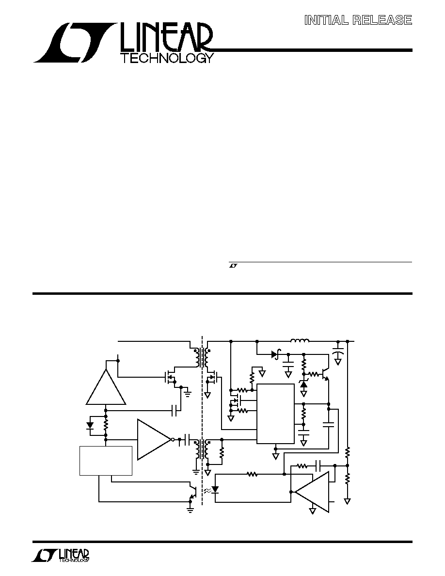
DESCRIPTIO
U
TYPICAL APPLICATIO
U
Synchronous Rectifier
Driver for Forward Converters
November 2003
The LTC
®
3900 is a secondary-side synchronous rectifier
driver designed to be used in isolated forward converter
power supplies. The chip drives N-channel rectifier
MOSFETs and accepts pulse sychronization from the
primary-side controller via a pulse transformer.
The LTC3900 incorporates a full range of protection for the
external MOSFETs. A programmable timeout function is
included that disables both drivers when the synchroniza-
tion signal is missing or incorrect. Additionally, the chip
senses the output inductor current through the drain-
source resistance of the catch MOSFET, shutting off the
MOSFET if the inductor current reverses. The LTC3900
also shuts off the drivers if the supply voltage is low.
, LTC and LT are registered trademarks of Linear Technology Corporation.
ISOLATION
BARRIER
T1
Q3
Q4
Q1
R
CS1
R
CS2
R
CS3
CS
+
CG
CS
FG
SYNC
V
CC
TIMER
LTC3900
R
TMR
R
SYNC
T2
C
SG
R1
R2
C
TMR
C
VCC
V
OUT
3.3V
V
IN
36V TO 72V
3900 F01
L0
D3
C
Z
R
Z
R
B
D
Z
C
OUT
Q
REG
+
GND
+
LT1950
FORWARD CONTROLLER
GND
COMP
OC1
LT1797
LTC1693-2
270
V
R
C
F
R
F
BG
SG
LTC1693-2
GATE
Figure 1. Simplified Isolated Forward Converter
LTC3900
2
3900i
Supply Voltage
V
CC .........................................................................................
12V
Input Voltage
CS
, TIMER .............................. 0.3V to (V
CC
+0.3V)
SYNC ...................................................... 12V to 12V
Input Current
CS
+ ....................................................................................
15mA
Operating Temperature Range (Note 2) ... 40
°
C to 85
°
C
Storage Temperature Range ................. 65
°
C to 150
°
C
Lead Temperature (Soldering, 10 sec).................. 300
°
C
ORDER PART
NUMBER
S8 PART
MARKING
T
JMAX
= 150
°
C,
JA
= 130
°
C/W
3900
LTC3900ES8
ABSOLUTE AXI U
RATI GS
W
W
W
U
PACKAGE/ORDER I FOR ATIO
U
U
W
(Note 1)
ELECTRICAL CHARACTERISTICS
The
q
denotes specifications which apply over the full operating
temperature range.
V
CC
= 5V, T
A
= 25
°
C unless otherwise specified. (Note 3)
Consult LTC Marketing for parts specified with wider operating temperature ranges.
TOP VIEW
SYNC
TIMER
GND
FG
CS
+
CS
CG
V
CC
S8 PACKAGE
8-LEAD PLASTIC SO
1
2
3
4
8
7
6
5
SYMBOL
PARAMETER
CONDITIONS
MIN
TYP
MAX
UNITS
V
CC
Supply Voltage Range
q
4.5
5
11
V
V
UVLO
V
CC
Undervoltage Lockout Threshold
Rising Edge
q
4.1
4.5
V
V
CC
Undervoltage Lockout Hysteresis
Rising Edge to Falling Edge
0.5
V
I
VCC
V
CC
Supply Current
V
SYNC
= 0V
q
0.5
1
mA
f
SYNC
= 100kHz, C
FG
= C
CG
= 4700pF (Note 4)
q
7
15
mA
Timer
V
TMR
Timer Threshold Voltage
q
10%
V
CC
/5
10%
V
I
TMR
Timer Input Current
V
TMR
= 0V
q
6
10
µ
A
t
TMRDIS
Timer Discharge Time
C
TMR
= 1000pF, R
TMR
= 4.7k
q
40
120
ns
V
TMRMAX
Timer Pin Clamp Voltage
C
TMR
= 1000pF, R
TMR
= 4.7k
2.5
V
Current Sense
I
CS
+
CS
+
Input Current
V
CS
+ = 0V
q
±
1
µ
A
I
CS
CS
Input Current
V
CS
= 0V
q
±
1
µ
A
V
CSMAX
CS
+
Pin Clamp Voltage
I
IN
= 5mA, V
SYNC
= 5V
11
V
V
CS
Current Sense Threshold Voltage
V
CS
= 0V
7.5
10.5
13.5
mV
(Note 6)
q
3
18
mV
SYNC Input
I
SYNC
SYNC Input Current
V
SYNC
=
±
10V
q
±
1
±
10
µ
A
V
SYNCP
SYNC Input Positive Threshold
q
1.0
1.4
1.8
V
SYNC Positive Input Hysteresis
(Note 5)
0.2
V
V
SYNCN
SYNC Input Negative Threshold
q
1.8
1.4
1.0
V
SYNC Negative Input Hysteresis
(Note 5)
0.2
V
LTC3900
3
3900i
ELECTRICAL CHARACTERISTICS
The
q
denotes specifications which apply over the full operating
temperature range.
V
CC
= 5V, T
A
= 25
°
C unless otherwise specified. (Note 3)
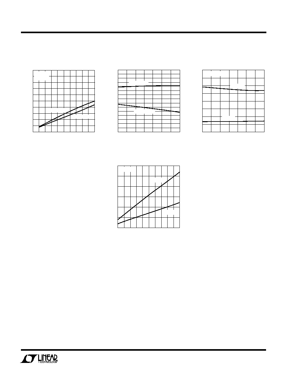
TYPICAL PERFOR A CE CHARACTERISTICS
U
W
Timeout vs V
CC
Timeout vs Temperature
Timeout vs R
TMR
Note 1: Absolute Maximum Ratings are those values beyond which the life
of a device may be impaired.
Note 2: The LTC3900E is guaranteed to meet performance specifications
from 0
°
C to 70
°
C. Specifications over the 40
°
C to 85
°
C operating
temperature range are assured by design; characterization and correlation
with statistical process controls.
Note 3: All currents into device pins are positive; all currents out of device
pins are negative. All voltages are referenced to ground unless otherwise
specified.
Note 4: Supply current in normal operation is dominated by the current
needed to charge and discharge the external MOSFET gates. This current
will vary with supply voltage, switching frequency and the external
MOSFETs used.
Note 5: Guaranteed by design, not subject to test.
Note 6: The current sense comparator threshold has a 0.33%/
°
C
temperature coefficient (TC) to match the TC of the external MOSFET
R
DS(ON)
.
Note 7: Rise and fall times are measured using 10% and 90% levels. Delay
times are measured from
±
1.4V at SYNC input to 20%/80% levels at the
driver output.
TIMEOUT (
µ
s)
5.25
5.20
5.15
5.10
5.05
5.00
4.95
4.90
4.85
4.80
4.75
V
CC
(V)
4
TIMEOUT (
µ
s)
5.25
5.20
5.15
5.10
5.05
5.00
4.95
4.90
4.85
4.80
4.75
6
8
9
3900 G01
5
7
10
11
TEMPERATURE (
°
C)
50
0
50
75
3900 G02
25
25
100
125
R
TMR
(k
)
10
9
8
7
6
5
4
3
2
1
0
TIMEOUT (
µ
s)
3900 G03
0
10 20 30 40
50 60 70
80 90 100
T
A
= 25
°
C
R
TMR
= 51k
C
TMR
= 470pF
T
A
= 25
°
C
V
CC
= 5V
C
TMR
= 470pF
V
CC
= 5V
R
TMR
= 51k
C
TMR
= 470pF
SYMBOL
PARAMETER
CONDITIONS
MIN
TYP
MAX
UNITS
Driver Output
R
ONH
Driver Pull-Up Resistance
I
OUT
= 100mA
0.9
1.2
q
1.6
R
ONL
Driver Pull-Down Resistance
I
OUT
= 100mA
0.9
1.2
q
1.6
I
PK
Driver Peak Output Current
(Note 5)
2
A
Switching Characteristics (Note 7)
t
d
SYNC Input to Driver Output Delay
C
FG
= C
CG
= 4700pF, V
SYNC
=
±
5V
q
60
120
ns
t
SYNC
Minimum SYNC Pulse Width
V
SYNC
=
±
5V
q
75
ns
t
r
, t
f
Driver Rise/Fall Time
C
FG
= C
CG
= 4700pF, V
SYNC
=
±
5V
15
ns
LTC3900
4
3900i
SYNC Negative Threshold vs
Temperature
V
CS(MAX)
Clamp Voltage vs CS
+
Input Current
Current Sense Threshold vs
Temperature
Propagation Delay vs V
CC
SYNC Positive Threshold vs
Temperature
Propagation Delay vs
Temperature
Propagation Delay vs C
LOAD
Rise/Fall Time vs V
CC
Rise/Fall Time vs Temperature
TYPICAL PERFOR A CE CHARACTERISTICS
U
W
CURRENT SENSE THRESHOLD (mV)
18
17
16
15
14
13
12
11
10
9
8
7
6
5
4
3
3900 G04
V
CC
= 5V, 11V
CS
+
INPUT CURRENT (mA)
0
5
V
CS(MAX)
CLAMP VOLTAGE (V)
10
20
15
25
30
3900 G05
18
17
16
15
14
13
12
11
10
TEMPERATURE (
°
C)
50
SYNC POSITIVE THRESHOLD (V)
100
3900 G06
0
50
1.8
1.7
1.6
1.5
1.4
1.3
1.2
1.1
1.0
25
25
75
125
TEMPERATURE (
°
C)
50
SYNC NEGATIVE THRESHOLD (V)
100
3900 G07
0
50
1.0
1.1
1.2
1.3
1.4
1.5
1.6
1.7
1.8
25
25
75
125
V
CC
(V)
4
PROPAGATION DELAY (
µ
s)
10
3900 G08
6
8
120
110
100
90
80
70
60
50
40
5
7
9
11
TEMPERATURE (
°
C)
50
100
3900 G09
0
50
25
25
75
125
50
100
0
50
25
25
75
125
C
LOAD
(nF)
1
2
3
10
3900 G10
4
5
6
7
9
8
RISE/FALL TIME (ns)
50
45
40
35
30
25
20
15
10
5
0
RISE/FALL TIME (ns)
50
45
40
35
30
25
20
15
10
5
0
3900 G11
TEMPERATURE (
°
C)
3900 G12
TEMPERATURE (
°
C)
50
100
0
50
25
25
75
125
T
A
= 25
°
C
T
A
= 25
°
C
C
LOAD
= 4.7nF
T
A
= 25
°
C
C
LOAD
= 4.7nF
T
A
= 25
°
C
V
CC
= 5V
V
CC
= 5V
C
LOAD
= 4.7nF
V
CC
= 5V
C
LOAD
= 4.7nF
V
CC
= 5V
V
CC
= 11V
V
CC
= 5V, 11V
SYNC TO FG
SYNC TO CG
SYNC TO FG
SYNC TO CG
SYNC TO FG
SYNC TO CG
PROPAGATION DELAY (
µ
s)
120
110
100
90
80
70
60
50
40
PROPAGATION DELAY (
µ
s)
120
110
100
90
80
70
60
50
40
V
CC
(V)
4
10
6
8
5
7
9
11
FALL TIME
FALL TIME
RISE TIME
RISE TIME
LTC3900
5
3900i
Rise/Fall Time vs Load
Capacitance
Undervoltage Lockout Threshold
Voltage vs Temperature
V
CC
Supply Current vs
Temperature
V
CC
Supply Current vs Load
Capacitance
TYPICAL PERFOR A CE CHARACTERISTICS
U
W
C
LOAD
(nF)
1
0
2
3
10
4
5
6
7
9
8
C
LOAD
(nF)
1
0
2
3
10
4
5
6
7
9
8
RISE/FALL TIME (ns)
50
45
40
35
30
25
20
15
10
5
0
T
A
= 25
°
C
V
CC
= 5V
T
A
= 25
°
C
FALL TIME
RISE TIME
UNDERVOLTAGE LOCKOUT THRESHOLD
VOLTAGE (V)
4.5
4.4
4.3
4.2
4.1
4.0
3.9
3.8
3.7
3.6
3.5
3.4
3.3
3.2
3.1
3.0
3900 G14
3900 G16
3900 G13
3900 G15
TEMPERATURE (
°
C)
50
100
0
50
25
25
75
125
FALLING EDGE
RISING EDGE
TEMPERATURE (
°
C)
50
100
0
50
25
25
75
125
C
LOAD
= 4.7nF
V
CC
SUPPLY CURRENT (mA)
20
18
16
14
12
10
8
6
4
V
CC
= 5V
V
CC
= 11V
V
CC
= 5V
V
CC
= 11V
SUPPLY CURRENT (mA)
30
25
20
15
10
5
0