LTC4075/LTC4075X
1
4075Xf
The LTC
Æ
4075/LTC4075X are standalone linear chargers
that are capable of charging a single-cell Li-Ion battery
from both wall adapter and USB inputs. The chargers can
detect power at the inputs and automatically select the
appropriate power source for charging.
No external sense resistor or blocking diode is required
for charging due to the internal MOSFET architecture.
Internal thermal feedback regulates the battery charge
current to maintain a constant die temperature during high
power operation or high ambient temperature conditions.
The fl oat voltage is fi xed at 4.2V and the charge current
is programmed with an external resistor. The LTC4075
terminates the charge cycle when the charge current drops
below the programmed termination threshold after the
fi nal fl oat voltage is reached. With power applied to both
inputs, the LTC4075/LTC4075X can be put into shutdown
mode reducing the DCIN supply current to 20µA, the USBIN
supply current to 10µA, and the battery drain current to
less than 2µA.
Other features include automatic recharge, undervoltage
lockout, charge status outputs, and "power present"
status outputs to indicate the presence of wall adapter
or USB power.
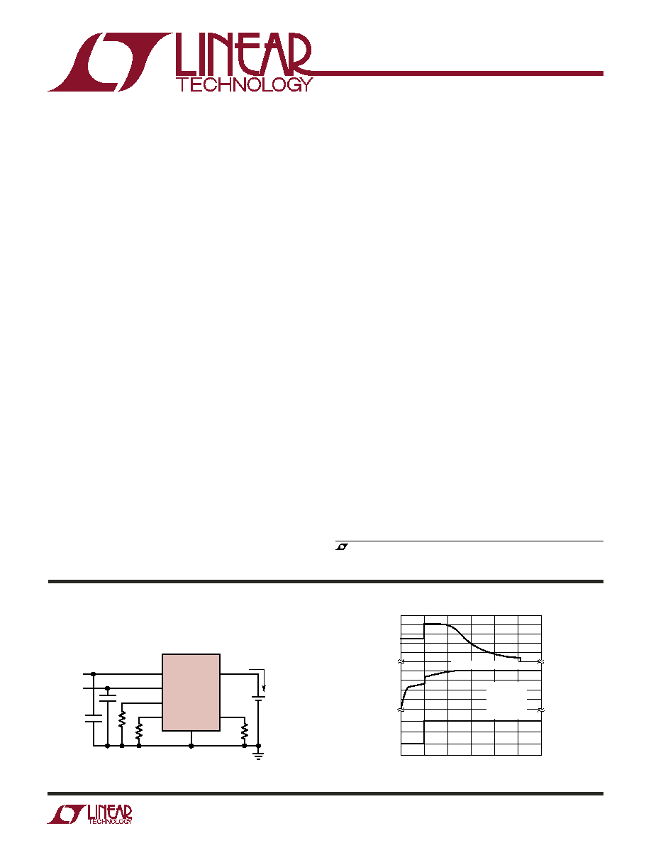
Dual Input Battery Charger for Single-Cell Li-Ion
LTC4075
DCIN
USBIN
IUSB
IDC
BAT
ITERM
1.24k
1%
2k
1%
2k
1%
WALL
ADAPTER
USB
PORT
1
µF
1
µF
+
4.2V
SINGLE CELL
Li-Ion BATTERY
800mA (WALL)
500mA (USB)
4075 TA01
GND
Dual Input USB/AC
Adapter Standalone Li-Ion
Battery Chargers
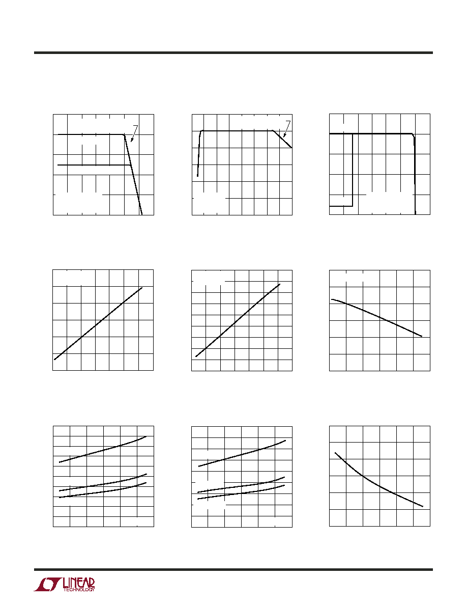
TIME (HR)
0
CHARGE
CURRENT (mA)
BATTERY
VOLTAGE (V)
DCIN
VOLTAGE (V)
4.2
200
0
400
800
600
1000
1.5
2.5
4075 TA01b
3.6
3.4
5.0
4.0
3.8
2.5
0
≠2.5
0.5
1.0
2.0
3.0
CONSTANT VOLTAGE
USBIN = 5V
T
A
= 25
∞C
R
IDC
= 1.25k
R
IUSB
= 2k
Complete Charge Cycle (1100mAh Battery)
, LTC and LT are registered trademarks of Linear Technology Corporation.
All other trademarks are the property of their respective owners.
*Protected by U.S. patents, including 6522118, 6700364
APPLICATIO S
U
FEATURES
DESCRIPTIO
U
TYPICAL APPLICATIO
U
Charges Single-Cell Li-Ion Batteries from Wall
Adapter and USB Inputs
Automatic Input Power Detection and Selection
Charge Current Programmable up to 950mA from
Wall Adapter Input
No External MOSFET, Sense Resistor or Blocking
Diode Needed
Thermal Regulation Maximizes Charging Rate
Without Risk of Overheating*
Preset Charge Voltage with ±0.6% Accuracy
Programmable Charge Current Termination
18µA USB Suspend Current in Shutdown
Independent "Power Present" Status Outputs
Charge Status Output
Automatic Recharge
Available Without Trickle Charge (LTC4075X)
Available in a Thermally Enhanced, Low Profi le
(0.75mm) 10-Lead (3mm ◊ 3mm) DFN Package
Cellular Telephones
Handheld Computers
Portable MP3 Players
Digital Cameras
LTC4075/LTC4075X
2
4075Xf
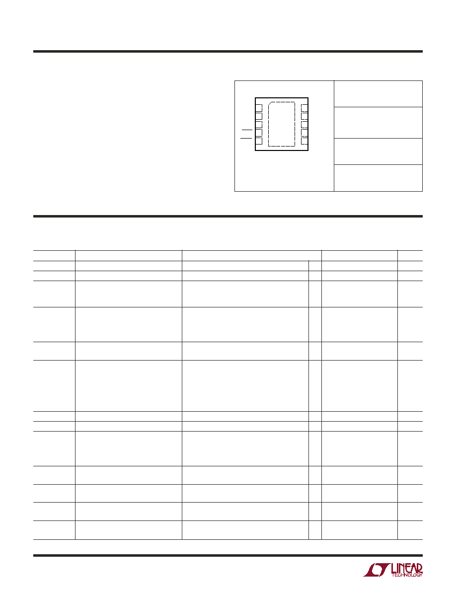
TOP VIEW
DD PACKAGE
10-LEAD (3mm
◊ 3mm) PLASTIC DFN
EXPOSED PAD IS GND (PIN 11)
MUST BE SOLDERED TO PCB
10
9
6
7
8
11
4
5
3
2
1
DCIN
BAT
IDC
USBPWR
ENABLE
USBIN
IUSB
ITERM
PWR
CHRG
SYMBOL PARAMETER
CONDITIONS
MIN
TYP
MAX
UNITS
V
DCIN
Supply
Voltage
4.3
8
V
V
USBIN
Supply
Voltage
4.3
8
V
I
DCIN
DCIN Supply Current
Charge Mode (Note 4), R
IDC
= 10k
250 800
µA
Standby Mode; Charge Terminated
50 100
µA
Shutdown Mode (ENABLE = 5V)
20
40
µA
I
USBIN
USBIN Supply Current
Charge Mode (Note 5), R
IUSB
= 10k, V
DCIN
= 0V
250 800
µA
Standby Mode; Charge Terminated, V
DCIN
= 0V
50 100
µA
Shutdown
(V
DCIN
= 0V, ENABLE = 0V)
18
36
µA
V
DCIN
> V
USBIN
10
20
µA
V
FLOAT
Regulated Output (Float) Voltage
I
BAT
=
1mA
4.175 4.2 4.225
V
I
BAT
= 1mA, 0∞C < T
A
<
85∞C
4.158 4.2 4.242
V
I
BAT
BAT
Pin
Current
R
IDC
= 1.25k, Constant-Current Mode
760 800 840 mA
R
IUSB
= 2.1k, Constant-Current Mode
450 476 500 mA
R
IDC
= 10k or R
IUSB
= 10k
93
100 107
mA
Standby Mode, Charge Terminated
≠3
≠ 6
µA
Shutdown
Mode
(Charger
Disabled)
≠1
≠ 2
µA
Sleep
Mode
(V
DCIN
= 0V, V
USBIN
= 0V)
±1
±2
µA
V
IDC
IDC Pin Regulated Voltage
Constant-Current Mode
0.95
1
1.05
V
V
IUSB
IUSB Pin Regulated Voltage
Constant-Current Mode
0.95
1
1.05
V
I
TERMINATE
Charge Current Termination Threshold
R
ITERM
= 1k
90
100 110
mA
R
ITERM
= 2k
45 50 55 mA
R
ITERM
= 10k
8.5
10
11.5
mA
R
ITERM
= 20k
4 5 6 mA
I
TRIKL
Trickle Charge Current (Note 6)
V
BAT
< V
TRIKL
; R
IDC
= 1.25k
60
80
100
mA
V
BAT
< V
TRIKL
; R
IUSB
=
2.1k
30 47.5 65 mA
V
TRIKL
Trickle Charge Threshold (Note 6)
V
BAT
Rising
2.8
2.9
3
V
Hysteresis
100
mV
V
UVDC
DCIN Undervoltage Lockout Voltage
From Low to High
4
4.15
4.3
V
Hysteresis
200
mV
V
UVUSB
USBIN Undervoltage Lockout Voltage
From Low to High
3.8
3.95
4.1
V
Hysteresis
200
mV
Input Supply Voltage (DCIN, USBIN) ........... ≠ 0.3 to 10V
EN, CHRG, PWR, USBPWR .......................... ≠ 0.3 to 10V
BAT, IDC, IUSB, ITERM .................................. ≠ 0.3 to 7V
DCIN Pin Current (Note 7) ..........................................1A
USBIN Pin Current (Note 7) .................................700mA
BAT Pin Current (Note 7) ............................................1A
BAT Short-Circuit Duration ............................ Continuous
Maximum Junction Temperature .......................... 125
∞
C
Operating Temperature Range (Note 2) .. ≠ 40
∞
C to 85
∞
C
Storage Temperature Range .................. ≠ 65
∞
C to 125
∞
C
ORDER PART
NUMBER
DD PART
MARKING
T
JMAX
= 125∞C,
JA
= 40∞C/W (NOTE 3)
Consult LTC Marketing for parts specifi ed with wider operating temperature ranges.
LBSC
LBRK
LTC4075EDD
LTC4075XEDD
(Note 1)
The
denotes the specifi cations which apply over the full operating
temperature range, otherwise specifi cations are at T
A
= 25∞C. V
DCIN
= 5V, V
USBIN
= 5V unless otherwise noted.
ELECTRICAL CHARACTERISTICS
ABSOLUTE AXI U
RATI GS
W
W
W
U
PACKAGE/ORDER I FOR ATIO
U
U
W
LTC4075/LTC4075X
3
4075Xf
SYMBOL PARAMETER
CONDITIONS
MIN
TYP
MAX
UNITS
V
ASD-DC
V
DCIN
≠ V
BAT
Lockout Threshold
V
DCIN
from Low to High, V
BAT
=
4.2V
140 180 220 mV
V
DCIN
from High to Low, V
BAT
=
4.2V
20 50 80 mV
V
ASD-USB
V
USBIN
≠ V
BAT
Lockout Threshold
V
USBIN
from Low to High
140
180
220
mV
V
USBIN
from High to Low
20
50
80
mV
V
ENABLE
ENABLE
Input
Threshold
Voltage
0.4
0.7
1 V
R
ENABLE
ENABLE Pulldown Resistance
1.2
2
5
M
V
CHRG
CHRG Output Low Voltage
I
CHRG
= 5mA
0.35
0.6
V
V
PWR
PWR Output Low Voltage
I
PWR
= 5mA
0.35
0.6
V
V
USBPWR
USBPWR
Output
Low
Voltage I
USBPWR
= 300µA
0.35
0.6
V
V
RECHRG
Recharge
Battery
Threshold
V
FLOAT
≠ V
RECHRG
, 0∞C < T
A
< 85∞C
65
100
135
mV
t
RECHRG
Recharge Comparator Filter Time
V
BAT
from High to Low
3
6
9
ms
t
TERMINATE
Termination Comparator Filter Time
I
BAT
Drops Below Termination Threshold
0.8
1.5
2.2
ms
t
SS
Soft-Start
Time
I
BAT
= 0 to Full-Scale
175
250
325
µs
R
ON-DC
Power FET "ON" Resistance
400
m
(Between DCIN and BAT)
R
ON-USB
Power FET "ON" Resistance
550
m
(Between USBIN and BAT)
T
LIM
Junction Temperature in
105
∞C
Constant-Temperature
Mode
The
denotes the specifi cations which apply over the full operating
temperature range, otherwise specifi cations are at T
A
= 25∞C. V
DCIN
= 5V, V
USBIN
= 5V unless otherwise noted.
Note 1: Absolute Maximum Ratings are those values beyond which the life
of a device may be impaired.
Note 2: The LTC4075E/LTC4075XE are guaranteed to meet the
performance specifi cations from 0∞C to 70∞C. Specifi cations over the
≠ 40∞C to 85∞C operating temperature range are assured by design,
characterization and correlation with statistical process controls.
Note 3: Failure to correctly solder the exposed backside of the package to
the PC board will result in a thermal resistance much higher than 40∞C/W.
See Thermal Considerations.
Note 4: Supply current includes IDC and ITERM pin current (approximately
100µA each) but does not include any current delivered to the battery
through the BAT pin.
Note 5: Supply current includes IUSB and ITERM pin current
(approximately 100µA each) but does not include any current delivered to
the battery through the BAT pin.
Note 6: This parameter is not applicable to the LTC4075X.
Note 7: Guaranteed by long term current density limitations.
ELECTRICAL CHARACTERISTICS
LTC4075/LTC4075X
4
4075Xf
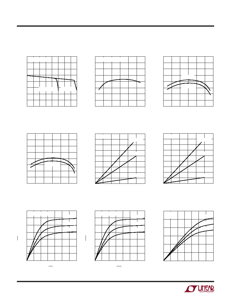
CHARGE CURRENT (mA)
0
V
FLOAT
(V)
800
500 600 700
400
4075X G01
100 200 300
4.26
4.24
4.22
4.20
4.18
4.16
4.14
4.12
4.10
4075X G04
TEMPERATURE (
∞C)
≠50
≠25
V
FLOAT
(V)
0
50
25
75
100
4075X G02
TEMPERATURE (
∞C)
≠50
≠25
0
50
25
75
100
TEMPERATURE (
∞C)
≠50
≠25
0
50
25
75
100
4.220
4.215
4.210
4.205
4.200
4.195
4.190
4.185
4.180
V
IDC
(V)
4075X G03
1.008
1.006
1.004
1.002
1.000
0.998
0.996
0.994
0.992
V
IUSB
(V)
1.008
1.006
1.004
1.002
1.000
0.998
0.996
0.994
0.992
V
IDC
(V)
0
0.2
0.6
1.0
I
BAT
(mA)
0.8
900
800
700
600
500
400
300
200
100
0
I
BAT
(mA)
900
800
700
600
500
400
300
200
100
0
4075X G05
0.4
1.2
V
IUSB
(V)
0
0.2
0.6
1.0
0.8
0.4
1.2
4075X G06
V
PWR
(V)
0
35
30
25
20
15
10
5
0
3
5
4075X G07
1
2
4
6
7
I
PWR
(mA)
4075X G08
R
IDC
= 1.25k
R
IDC
= R
IUSB
= 2k
V
DCIN
= V
USBIN
= 5V
V
DCIN
= V
USBIN
= 5V
V
DCIN
= V
USBIN
= 5V
V
DCIN
= V
USBIN
= 5V
V
DCIN
= 5V
V
DCIN
= 8V
V
DCIN
= 4.3V
V
USBIN
= 8V
V
USBIN
= 4.3V
R
IDC
= 1.25k
V
USBIN
= 5V
R
IUSB
= 1.25k
R
IUSB
= 2k
R
IUSB
= 10k
R
IDC
= 2k
R
IDC
= 10k
35
30
25
20
15
10
5
0
I
CHRG
(mA)
T
A
= ≠ 40
∞C
T
A
= 25
∞C
T
A
= 90
∞C
T
A
= ≠ 40
∞C
T
A
= ≠ 40
∞C
T
A
= 25
∞C
T
A
= 25
∞C
T
A
= 90
∞C
T
A
= 90
∞C
V
CHRG
(V)
0
3
5
1
2
4
6
7
V
USBPWR
(V)
0
I
USBPWR
(mA)
6
5
4
3
2
1
0
3
5
4075X G09
1
2
4
6
7
V
DCIN
= 5V
V
USBIN
= 0V
IUSB Pin Voltage vs Temperature
(Constant-Current Mode)
Charge Current vs IDC Pin
Voltage
Charge Current vs IUSB Pin
Voltage
PWR Pin I-V Curve
CHRG Pin I-V Curve
USBPWR Pin I-V Curve
Regulated Output (Float) Voltage
vs Charge Current
Regulated Output (Float) Voltage
vs Temperature
IDC Pin Voltage vs Temperature
(Constant-Current Mode)
TYPICAL PERFOR A CE CHARACTERISTICS
U
W
LTC4075/LTC4075X
5
4075Xf
I
BAT
(mA)
1000
800
600
400
200
0
4075X G10
V
DCIN
(V)
I
BAT
(mA)
4075X G11
900
800
700
600
500
400
300
4.0
5.0
6.0
6.5
4.5
5.5
7.0
7.5
8.0
TEMPERATURE (
∞C)
≠50
R
DS(ON)
(m
)
550
500
450
400
350
300
250
25
75
4075X G13
≠25
0
50
100
125
TEMPERATURE (
∞C)
≠50
25
75
≠25
0
50
100
125
TEMPERATURE (
∞C)
≠50
25
75
≠25
0
50
100
125
TEMPERATURE (
∞C)
≠50
25
75
≠25
0
50
100
TEMPERATURE (
∞C)
≠50
25
75
≠25
0
50
100
TEMPERATURE (
∞C)
≠50
25
75
≠25
0
50
100
TEMPERATURE (
∞C)
≠50
25
75
≠25
0
50
100
R
DS(ON)
(m
)
800
750
700
650
600
550
500
450
400
350
4075X G14
V
ENABLE
(mV)
900
850
800
750
700
650
600
I
DCIN
(
µ
A)
4075X G16
50
45
40
35
30
25
20
15
10
5
0
I
USBIN
(
µ
A)
45
40
35
30
25
20
15
10
5
0
4075X G17
4075X G18
R
ENABLE
(M
)
2.8
2.6
2.4
2.2
2.0
1.8
1.6
4075X G15
V
DCIN
= 8V
V
DCIN
= 5V
V
DCIN
= 4.3V
V
USBIN
= 8V
V
USBIN
= 5V
V
USBIN
= 4.3V
ENABLE = 5V
ENABLE = 0V
V
DCIN
= V
USBIN
= 5V
V
BAT
= 4V
JA
= 40
∞C/W
V
BAT
= 4V
I
BAT
= 200mA
V
BAT
= 4V
I
BAT
= 200mA
R
IDC
= 1.25k
V
BAT
= 4V
JA
= 35
∞C/W
R
IDC
= 1.25k
R
IDC
= R
IUSB
= 2k
ONSET OF
THERMAL REGULATION
ONSET OF
THERMAL REGULATION
V
DCIN
= V
USBIN
= 5V
V
BAT
(V)
2.4
I
BAT
(mA)
1000
800
600
400
200
0
3.0
3.6
3.9
4075X G12
2.7
3.3
4.2
4.5
LTC4075
LTC4075X
V
DCIN
= V
USBIN
= 5V
JA
= 40
∞C/W
R
IDC
= 1.25k
Charge Current vs Ambient
Temperature
Charge Current vs
Supply Voltage
Charge Current vs Battery Voltage
DCIN Power FET "On" Resistance
vs Temperature
USBIN Power "On" Resistance
vs Temperature
ENABLE Pin Threshold (On-to-Off)
vs Temperature
DCIN Shutdown Current vs
Temperature
USBIN Shutdown Current vs
Temperature
ENABLE Pin Pulldown Resistance
vs Temperature
TYPICAL PERFOR A CE CHARACTERISTICS
U
W