Äîêóìåíòàöèÿ è îïèñàíèÿ www.docs.chipfind.ru
1
LTC4211
4211f
APPLICATIO S
U
DESCRIPTIO
U
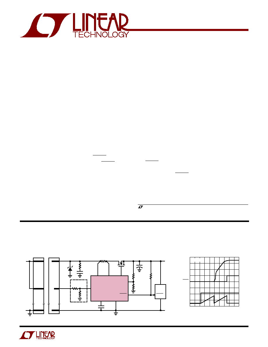
TYPICAL APPLICATIO
U
FEATURES
s
Allows Safe Board Insertion and Removal
from a Live Backplane
s
Controls Supply Voltages from 2.5V to 16.5V
s
Programmable Soft-Start with Inrush Current
Limiting, No External Gate Capacitor Required
s
Faster Turn-Off Time Because No External Gate
Capacitor is Required
s
Dual Level Overcurrent Fault Protection
s
Programmable Response Time for Overcurrent
Protection (MS)
s
Programmable Overvoltage Protection (MS)
s
Automatic Retry or Latched Mode Operation (MS)
s
High Side Drive for an External N-Channel FET
s
User-Programmable Supply Voltage Power-Up Rate
s
FB Pin Monitors V
OUT
and Signals RESET
s
Glitch Filter Protects Against Spurious RESET Signal
The LTC
®
4211 is a Hot Swap
TM
controller that allows a
board to be safely inserted and removed from a live
backplane. An internal high side switch driver controls the
gate of an external N-channel MOSFET for supply voltages
ranging from 2.5V to 16.5V. The LTC4211 provides soft-
start and inrush current limiting during the start-up period
which has a programmable duration.
Two on-chip current limit comparators provide dual level
overcurrent circuit breaker protection. The slow com-
parator trips at V
CC
50mV and activates in 20
µ
s (or
programmed by an external filter capacitor, MS only). The
fast comparator trips at V
CC
150mV and typically
responds in 300ns.
The FB pin monitors the output supply voltage and signals
the RESET output pin. The ON pin signal turns the chip on
and off and can also be used for the reset function. The
MS package has FAULT and FILTER pins to provide
additional functions like fault indication, autoretry or
latch-off modes, programmable current limit response
time and programmable overvoltage protection using an
external Zener diode clamp.
s
Electronic Circuit Breaker
s
Hot Board Insertion and Removal (Either On
Backplane or On Removable Card)
s
Industrial High Side Switch/Circuit Breaker
Hot Swap Controller with
Multifunction Current Control
, LTC and LT are registered trademarks of Linear Technology Corporation.
Single Channel 5V Hot Swap Controller
+
V
CC
SENSE
LTC4211
8
2
3
4
7
6
C
LOAD
V
OUT
5V
5A
GND
4211 TA01A
5
1
R4
15k
GATE
GND
TIMER
PCB CONNECTION SENSE
C
TIMER
10nF
FB
ON
SHORT
LONG
V
CC
5V
GND
LONG
Z1 = 1SMA10A OR SMAJ10A
* OPTIONAL
RESET
R2
10k
R1
20k
R
X
10
R
SENSE
0.007
PCB EDGE
CONNECTOR
(MALE)
M1
Si4410DY
Z1*
R3
36k
R5
10k
µ
P
LOGIC
RESET
C
X
100nF
BACKPLANE
CONNECTOR
(FEMALE)
Hot Swap is a trademark of Linear Technology Corporation.
4211 TA01b
2.5ms/DIV
NO C
LOAD
V
GATE
5V/DIV
V
RESET
5V/DIV
V
ON
1V/DIV
V
TIMER
1V/DIV
Power-Up Sequence
2
LTC4211
4211f
T
JMAX
= 125
°
C,
JA
= 150
°
C/ W
ORDER PART
NUMBER
Supply Voltage (V
CC
) ............................................... 17V
Input Voltage
FB, ON .................................................. 0.3V to 17V
SENSE, FILTER .......................... 0.3V to V
CC
+ 0.3V
TIMER ..................................................... 0.3V to 2V
Output Voltage
GATE ............................... Internally Limited (Note 3)
RESET, FAULT ...................................... 0.3V to 17V
Consult LTC Marketing for parts specified with wider operating temperature ranges.
LTC4211CS8
LTC4211IS8
ABSOLUTE AXI U RATI GS
W
W
W
U
PACKAGE/ORDER I FOR ATIO
U
U
W
(Note 1)
Operating Temperature Range
LTC4211C .............................................. 0
°
C to 70
°
C
LTC4211I ........................................... 40
°
C to 85
°
C
Storage Temperature Range ................. 65
°
C to 150
°
C
Lead Temperature (Soldering, 10 sec).................. 300
°
C
1
2
3
4
8
7
6
5
TOP VIEW
V
CC
SENSE
GATE
FB
RESET
ON
TIMER
GND
S8 PACKAGE
8-LEAD PLASTIC SO
S8 PART
MARKING
4211
4211I
ORDER PART
NUMBER
LTC4211CMS8
LTC4211IMS8
MS8 PART
MARKING
LTSC
LTSD
T
JMAX
= 125
°
C,
JA
= 200
°
C/ W
1
2
3
4
RESET
ON
TIMER
GND
8
7
6
5
V
CC
SENSE
GATE
FB
TOP VIEW
MS8 PACKAGE
8-LEAD PLASTIC MSOP
ORDER PART
NUMBER
LTC4211CMS
LTC4211IMS
MS PART
MARKING
LTSU
LTSV
T
JMAX
= 125
°
C,
JA
= 200
°
C/ W
1
2
3
4
5
RESET
ON
FILTER
TIMER
GND
10
9
8
7
6
FAULT
V
CC
SENSE
GATE
FB
TOP VIEW
MS PACKAGE
10-LEAD PLASTIC MSOP
SYMBOL
PARAMETER
CONDITIONS
MIN
TYP
MAX
UNITS
V
CC
V
CC
Supply Voltage Range
q
2.5
16.5
V
I
CC
V
CC
Supply Current
FB = High, ON = High, TIMER = Low
q
1
1.5
mA
V
LKO
Internal V
CC
Undervoltage Lockout
V
CC
Low-to-High Transition
q
2.13
2.3
2.47
V
V
LKOHST
V
CC
Undervoltage Lockout Hysteresis
120
mV
I
INFB
FB Input Current
V
FB
= V
CC
or GND
±
1
±
10
µ
A
I
INON
ON Input Current
V
ON
= V
CC
or GND
±
1
±
10
µ
A
I
LEAK
RESET, FAULT Leakage Current
V
RESET
= V
FAULT
= 15V, Pull-Down Device Off
q
±
0.1
±
2.5
µ
A
I
INSENSE
SENSE Input Current
V
SENSE
= V
CC
or GND
±
1
±
10
µ
A
V
CB(FAST)
SENSE Trip Voltage (V
CC
V
SENSE
)
Fast Comparator Trips
q
130
150
170
mV
V
CB(SLOW)
SENSE Trip Voltage (V
CC
V
SENSE
)
Slow Comparator Trips
q
40
50
60
mV
I
GATEUP
GATE Pull-Up Current
Charge Pump On, V
GATE
0.2V
q
12.5
10
7.5
µ
A
I
GATEDOWN
Normal GATE Pull-Down Current
ON Low
q
130
200
270
µ
A
Fast GATE Pull-Down Current
FAULT Latched and Circuit Breaker
50
mA
Tripped or in UVLO
The
q
denotes specifications which apply over the full operating
temperature range, otherwise specifications are T
A
= 25
°
C. V
CC
= 5V, unless otherwise noted. (Note 2)
ELECTRICAL CHARACTERISTICS
3
LTC4211
4211f
SYMBOL
PARAMETER
CONDITIONS
MIN
TYP
MAX
UNITS
V
GATE
External N-Channel Gate Drive
V
GATE
V
CC
(For V
CC
= 2.5V)
q
4.0
8
V
V
GATE
V
CC
(For V
CC
= 2.7V)
q
4.5
8
V
V
GATE
V
CC
(For V
CC
= 3.3V)
q
5.0
10
V
V
GATE
V
CC
(For V
CC
= 5V)
q
10
16
V
V
GATE
V
CC
(For V
CC
= 12V)
q
10
18
V
V
GATE
V
CC
(For V
CC
= 15V)
q
8
18
V
V
GATEOV
GATE Overvoltage Lockout Threshold
q
0.08
0.2
0.3
V
V
FB
FB Voltage Threshold
FB High to Low
q
1.223
1.236
1.248
V
V
FB
FB Threshold Line Regulation
2.5V
V
CC
16.5V
q
0.5
5
mV
V
FBHST
FB Voltage Threshold Hysteresis
3
mV
V
ONHI
ON Threshold High
q
1.23
1.316
1.39
V
V
ONLO
ON Threshold Low
q
1.20
1.236
1.26
V
V
ONHST
ON Hysteresis
80
mV
I
FILTER
FILTER Current
During Slow Fault Condition
q
2.5
2
1.5
µ
A
During Normal and Reset Conditions
q
7
10
13
µ
A
V
FILTER
FILTER Threshold
Latched Off Threshold, FILTER Low to High
q
1.20
1.236
1.26
V
V
FILTERHST
FILTER Threshold Hysteresis
80
mV
I
TMR
TIMER Current
Timer On, V
TIMER
= 1V
q
2.5
2
1.5
µ
A
Timer Off, TIMER = 1.5V
3
mA
V
TMR
TIMER Threshold
TIMER Low to High
q
1.20
1.236
1.26
V
TIMER High to Low
q
0.15
0.200
0.40
V
V
FAULT
FAULT Threshold
Latched Off Threshold, FAULT High to Low
q
1.20
1.236
1.26
V
V
FAULTHST
FAULT Threshold Hysteresis
50
mV
V
OLFAULT
Output Low Voltage
I
FAULT
= 1.6mA
q
0.14
0.4
V
V
OLRESET
Output Low Voltage
I
RESET
= 1.6mA
q
0.14
0.4
V
t
FAULTFC
FAST COMP Trip to GATE Discharging
V
CB
= 0mV to 200mV Step
q
300
700
ns
t
FAULTSC
SLOW COMP Trip to GATE Discharging V
CB
= 0mV to 100mV Step,
q
10
20
30
µ
s
8-Pin Version or FILTER Floating
V
CB
= 0mV to 100mV Step,
q
4
6
8
ms
10nF at FILTER Pin to GND
t
EXTFAULT
FAULT Low to GATE Discharging
V
FAULT
= 5V to 0V
q
1
3
5
µ
s
t
FILTER
FILTER High to FAULT Latched
V
FILTER
= 0V to 5V
q
2
4.5
7
µ
s
t
RESET
Circuit Breaker Reset Delay Time
ON Low to FAULT High
q
150
250
µ
s
t
OFF
Turn-Off Time
ON Low to GATE Off
8
µ
s
The
q
denotes specifications which apply over the full operating
temperature range, otherwise specifications are T
A
= 25
°
C. V
CC
= 5V, unless otherwise noted. (Note 2)
ELECTRICAL CHARACTERISTICS
Note 1: Absolute Maximum Ratings are those values beyond which the life
of a device may be impaired.
Note 2: All current into device pins are positive; all current out of device
pins are negative; all voltages are referenced to ground unless otherwise
specified.
Note 3: An internal Zener at the GATE pin clamps the charge pump voltage
to a typical maximum operating voltage of 26V. External voltage applied to
the GATE pin beyond the internal Zener voltage may damage the part. If a
lower GATE pin voltage is desired, use an external Zener diode. The GATE
capacitance must be < 0.15
µ
F at maximum V
CC
.
4
LTC4211
4211f
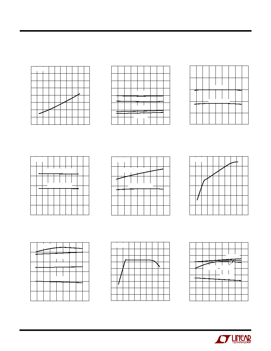
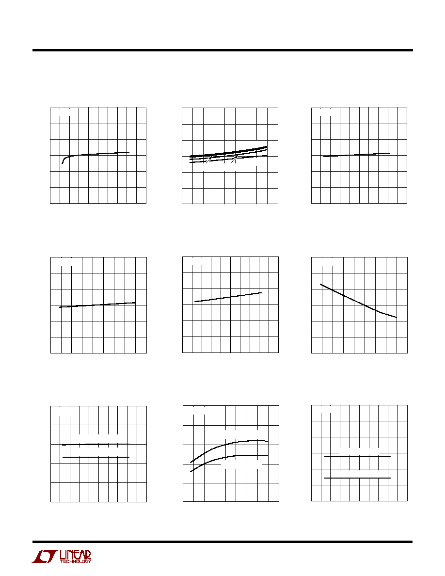
TYPICAL PERFOR A CE CHARACTERISTICS
U
W
Supply Current vs Supply Voltage
Supply Current vs Temperature
Undervoltage Lockout Threshold
vs Temperature
SUPPLY VOLTAGE (V)
0
SUPPLY CURRENT (mA)
4.0
3.5
3.0
2.5
2.0
1.5
1.0
0.5
0
16
4211 G01
4
8
12
20
14
2
6
10
18
T
A
= 25
°
C
TEMPERATURE (
°
C)
75
SUPPLY CURRENT (mA)
2.0
2.5
3.0
125
4211 G02
1.5
1.0
0
25
25
75
50
150
0
50
100
0.5
4.0
3.5
V
CC
= 15V
V
CC
= 12V
V
CC
= 5V
V
CC
= 3V
TEMPERATURE (
°
C)
75
2.0
UNDERVOLTAGE LOCKOUT THRESHOLD (V)
2.1
2.3
2.4
2.5
25
25
50
150
4211 G03
2.2
50
0
75 100 125
FALLING EDGE
RISING EDGE
ON Pin Threshold
vs Supply Voltage
ON Pin Threshold
vs Temperature
GATE Voltage vs Supply Voltage
SUPPLY VOLTAGE (V)
1.10
ON PIN THRESHOLD (V)
1.20
1.30
1.40
1.15
1.25
1.35
4
8
12
16
4211 G04
20
2
0
6
10
14
18
T
A
= 25
°
C
HIGH THRESHOLD
LOW THRESHOLD
TEMPERATURE (
°
C)
75
1.10
ON PIN THRESHOLD (V)
1.15
1.25
1.30
1.35
25
25
50
150
4211 G05
1.20
50
0
75 100 125
1.40
V
CC
= 5V
HIGH THRESHOLD
LOW THRESHOLD
SUPPLY VOLTAGE (V)
0
GATE VOLTAGE (V)
10
20
30
5
15
25
4
8
12
16
4211 G06
20
2
0
6
10
14
18
T
A
= 25
°
C
GATE Voltage vs Temperature
V
GATE
V
CC
vs Supply Voltage
V
GATE
V
CC
vs Temperature
TEMPERATURE (
°
C)
75
0
GATE VOLTAGE (V)
5
15
20
25
25
25
50
150
4211 G07
10
50
0
75 100 125
30
V
CC
= 15V
V
CC
= 12V
V
CC
= 5V
V
CC
= 3V
SUPPLY VOLTAGE (V)
0
0
V
GATE
V
CC
(V)
2
6
8
10
12 14 16 18
18
4211 G08
4
2
4
6
8
10
20
12
14
16
T
A
= 25
°
C
TEMPERATURE (
°
C)
75
0
V
GATE
V
CC
(V)
2
6
8
10
75
18
4211 G09
4
0
150
25
50
100
50
25
125
12
14
16
V
CC
= 12V
V
CC
= 15V
V
CC
= 5V
V
CC
= 3V
5
LTC4211
4211f
TYPICAL PERFOR A CE CHARACTERISTICS
U
W
GATE Output Source Current
vs Supply Voltage
Normal GATE Pull-Down Current
vs Supply Voltage
Normal GATE Pull-Down Current
vs Temperature
Fast GATE Pull-Down Current
vs Supply Voltage
Feedback Threshold
vs Supply Voltage
Feedback Threshold
vs Temperature
FILTER Threshold
vs Supply Voltage
GATE Output Source Current
vs Temperature
SUPPLY VOLTAGE (V)
7
GATE OUTPUT SOURCE CURRENT (
µ
A)
9
11
13
8
10
12
4
8
12
16
4211 G10
20
2
0
6
10
14
18
T
A
= 25
°
C
TEMPERATURE (
°
C)
75
7
GATE OUTPUT SOURCE CURRENT (
µ
A)
8
10
11
12
25
25
50
150
4211 G11
9
50
0
75 100 125
13
V
CC
= 15V
V
CC
= 3V
V
CC
= 5V
V
CC
= 12V
SUPPLY VOLTAGE (V)
140
NORMAL GATE PULL-DOWN CURRENT (
µ
A)
180
220
260
160
200
240
4
8
12
16
4211 G12
20
2
0
6
10
14
18
T
A
= 25
°
C
TEMPERATURE (
°
C)
75
140
NORMAL GATE PULL-DOWN CURRENT (
µ
A)
160
200
220
240
25
25
50
150
4211 G13
180
50
0
75 100 125
260
V
CC
= 5V
SUPPLY VOLTAGE (V)
20
FAST GATE PULL-DOWN CURRENT (mA)
40
60
80
30
50
70
4
8
12
16
4211 G14
20
2
0
6
10
14
18
T
A
= 25
°
C
Fast GATE Pull-Down Current
vs Temperature
TEMPERATURE (
°
C)
75
20
FAST GATE PULL-DOWN CURRENT (mA)
30
50
60
70
25
25
50
150
4211 G15
40
50
0
75 100 125
80
V
CC
= 5V
SUPPLY VOLTAGE (V)
0
FEEDBACK THRESHOLD (V)
1.240
1.245
1.250
16
4211 G16
1.235
1.230
1.225
4
8
12
2
18
6
10
14
20
T
A
= 25
°
C
HIGH THRESHOLD
LOW THRESHOLD
TEMPERATURE (
°
C)
75
1.225
FEEDBACK THRESHOLD (V)
1.230
1.240
1.245
1.250
25
25
50
150
4211 G17
1.235
50
0
75 100 125
V
CC
= 5V
HIGH THRESHOLD
LOW THRESHOLD
SUPPLY VOLTAGE (V)
1.10
FILTER THRESHOLD (V)
1.20
1.30
1.40
1.15
1.25
1.35
4
8
12
16
4211 G18
20
2
0
6
10
14
18
T
A
= 25
°
C
HIGH THRESHOLD
LOW THRESHOLD