 | –≠–ª–µ–∫—Ç—Ä–æ–Ω–Ω—ã–π –∫–æ–º–ø–æ–Ω–µ–Ω—Ç: LTC4213 | –°–∫–∞—á–∞—Ç—å:  PDF PDF  ZIP ZIP |
LTC4213
1
4213f
APPLICATIO S
U
TYPICAL APPLICATIO
U
DESCRIPTIO
U
FEATURES
The LTC
Æ
4213 is an Electronic Circuit Breaker. An over-
current circuit breaker senses the voltage across the drain
and source terminals of an external N-channel MOSFET
with no need for a sense resistor. The advantages are a
lower cost and reduced voltage and power loss in the
switch path. An internal high-side driver controls the
external MOSFET gate.
Two integrated comparators provide dual level over-
current protection over the bias supply to ground common
mode range. The slow comparator has 16µs response
while the fast comparator trips in 1µs. The circuit breaker
has three selectable trip thresholds: 25mV, 50mV and
100mV. An ON pin controls the ON/OFF and resets circuit
breaker faults. READY signals the MOSFET is conducting
and the circuit breaker is armed. The LTC4213 operates
from V
CC
= 2.3V to 6V.
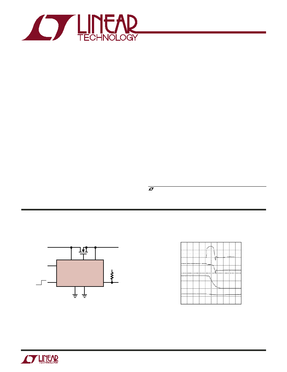
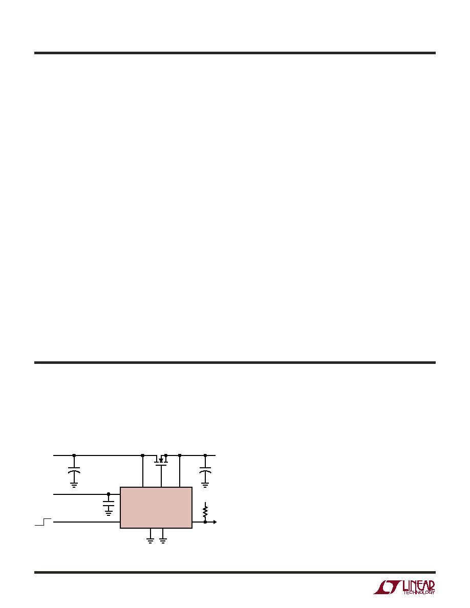
Electronic Circuit Breaker
High-Side Switch
Hot Board Insertion
Fast 1µs Response Circuit Breaker
3 Selectable Circuit Breaker Thresholds
No Sense Resistor Required
Dual Level Overcurrent Fault Protection
Controls Load Voltages from 0V to 6V
High Side Drive for External N-Channel FET
Undervoltage Lockout
READY Pin Signals When Circuit Breaker Armed
Small Plastic (3mm x 2mm) DFN Package
No R
SENSE
TM
Electronic Circuit Breaker
1.25V Electronic Circuit Breaker
OFF ON
LTC4213
V
CC
ON
READY
10k
I
SEL
GND
GATE
SI4864DY
V
BIAS
V
OUT
1.25V
3.5A
V
IN
1.25V
V
BIAS
2.3V TO 6V
SENSEN
SENSEP
4213 TA01
, LTC and LT are registered trademarks of Linear Technology Corporation.
No R
SENSE
is a trademark of Linear Technology Corporation. All other trademarks are the
property of their respective owners.
Severe Overload Response
2µs/DIV
4213 TA01b
I
OUT
(50A/DIV)
V
GATE
(5V/DIV)
V
OUT
(1V/DIV)
V
IN
(1V/DIV)
LTC4213
2
4213f
Bias Supply Voltage (V
CC
) ........................... ≠0.3V to 9V
Input Voltages
ON, SENSEP, SENSEN .............................≠ 0.3V to 9V
I
SEL
.......................................... ≠ 0.3V to (V
CC
+ 0.3V)
Output Voltages
GATE .....................................................≠ 0.3V to 15V
READY .....................................................≠ 0.3V to 9V
Operating Temperature Range
LTC4213C ............................................... 0∞C to 70∞C
LTC4213I ............................................. ≠40∞C to 85∞C
Storage Temperature Range ................. ≠ 65∞C to 150∞C
Lead Temperature (Soldering, 10sec)................... 300∞C
ORDER PART
NUMBER
DDB PART*
MARKING
T
JMAX
= 125∞C,
JA
= 250∞C/W
EXPOSED PAD (PIN 9)
PCB CONNECTION OPTIONAL
Consult LTC Marketing for parts specified with wider operating temperature ranges.
*The temperature grade is identified by a label on the shipping container.
LBHV
LTC4213CDDB
LTC4213IDDB
ABSOLUTE AXI U
RATI GS
W
W
W
U
PACKAGE/ORDER I FOR ATIO
U
U
W
(Note 1)
ELECTRICAL CHARACTERISTICS
The
denotes the specifications which apply over the full operating
temperature range, otherwise specifications are at T
A
= 25∞C. V
CC
= 5V, I
SEL
= 0 unless otherwise noted. (Note 2)
SYMBOL
PARAMETER
CONDITIONS
MIN
TYP
MAX
UNITS
V
CC
Bias Supply Voltage
2.3
6
V
V
SENSEP
SENSEP Voltage
0
6
V
I
CC
V
CC
Supply Current
1.6
3
mA
V
CC(UVLR)
V
CC
Undervoltage Lockout Release
V
CC
Rising
1.8
2.07
2.23
V
V
CC(UVHYST)
V
CC
Undervoltage Lockout Hysteresis
30
100
160
mV
I
SENSEP
SENSEP Input Current
V
SENSEP
= V
SENSEN
= 5V, Normal Mode
15
40
80
µA
V
SENSEP
= V
SENSEN
= 0, Normal Mode
≠1
±15
µA
I
SENSEN
SENSEN Input Current
V
SENSEP
= V
SENSEN
= 5V, Normal Mode
15
40
80
µA
V
SENSEP
= V
SENSEN
= 0, Normal Mode
≠1
±15
µA
V
SENSEP
= V
SENSEN
= 5V,
50
280
µA
Reset Mode or Fault Mode
V
CB
Circuit Breaker Trip Voltage
I
SEL
= 0, V
SENSEP
= V
CC
22.5
25
27.5
mV
V
CB
= V
SENSEP
≠ V
SENSEN
I
SEL
= Floated, V
SENSEP
= V
CC
45
50
55
mV
I
SEL
= V
CC,
V
SENSEP
= V
CC
90
100
110
mV
V
CB(FAST)
Fast Circuit Breaker Trip Voltage
I
SEL
= 0, V
SENSEP
= V
CC
63
100
115
mV
V
CB(FAST)
= V
SENSEP
≠ V
SENSEN
I
SEL
= Floated, V
SENSEP
= V
CC
126
175
200
mV
I
SEL
= V
CC,
V
SENSEP
= V
CC
252
325
371
mV
I
GATE(UP)
GATE Pin Pull Up Current
V
GATE
= 0V
≠50
≠100
≠150
µA
I
GATE(DN)
GATE Pin Pull Down Current
V
SENSEP
≠ V
SENSEN
= 200mV, V
GATE
= 8V
10
40
mA
V
GSMAX
External N-Channel Gate Drive
V
SENSEN
= 0, V
CC
2.97V, I
GATE
= ≠1µA
4.8
6.5
8
V
V
SENSEN
= 0, V
CC
= 2.3V, I
GATE
= ≠1µA
2.65
4.3
8
V
V
GSARM
V
GS
Voltage to Arm Circuit Breaker
V
SENSEN
= 0, V
CC
2.97V
4.4
5.4
7.6
V
V
SENSEN
= 0, V
CC
= 2.3V
2.5
3.5
7
V
TOP VIEW
DDB PACKAGE
8-LEAD (3mm ◊ 2mm) PLASTIC DFN
5
6
7
8
9
4
3
2
1
READY
ON
I
SEL
GND
V
CC
SENSEP
SENSEN
GATE
LTC4213
3
4213f
V
GSMAX
≠ V
GSARM
Difference Between V
GSMAX
and
V
SENSEN
= 0, V
CC
2.97V
0.3
1.1
V
V
GSARM
V
SENSEN
= 0, V
CC
= 2.3V
0.15
0.8
V
V
READY(OL)
READY Pin Output Low Voltage
I
READY
= 1.6mA, Pull Down Device On
0.2
0.4
V
I
READY(LEAK)
READY Pin Leakage Current
V
READY
= 5V, Pull Down Device Off
0
±1
µA
V
ON(TH)
ON Pin High Threshold
ON Rising, GATE Pulls Up
0.76
0.8
0.84
V
V
ON(HYST)
ON Pin Hysteresis
ON Falling, GATE Pulls Down
10
40
90
mV
V
ON(RST)
ON Pin Reset Threshold
ON Falling, Fault Reset, GATE Pull Down
0.36
0.4
0.44
V
I
ON(IN)
ON Pin Input Current
V
ON
= 1.2V
0
±1
µA
V
OV
Overvoltage Threshold
0.41
0.7
1.1
V
V
OV
= V
SENSEP
≠ V
CC
t
OV
Overvoltage Protection Trip Time
V
SENSEP
= V
SENSEN
= Step 5V to 6.2V
25
65
160
µs
t
FAULT(SLOW)
V
CB
Trips to GATE Discharging
V
SENSE
Step 0mV to 50mV,
7
16
27
µs
V
SENSEN
Falling, V
CC
= V
SENSEP
= 5V
t
FAULT(FAST)
V
CB(FAST)
Trips to GATE Discharging
V
SENSE
Step 0V to 0.3V, V
SENSEN
Falling,
1
2.5
µs
V
SENSEP
= 5V
t
DEBOUNCE
Startup De-Bounce Time
V
ON
= 0V to 2V Step to Gate Rising,
27
60
130
µs
(Exiting Reset Mode)
t
READY
READY Delay Time
V
GATE
= 0V to 8V Step to READY Rising,
22
50
115
µs
V
SENSEP
= V
SENSEN
= 0
t
OFF
Turn-Off Time
V
ON
= 2V to 0.6V Step to GATE Discharging
1.5
5
10
µs
t
ON
Turn-On Time
V
ON
= 0.6V to 2V Step to GATE Rising,
4
8
16
µs
(Normal Mode)
t
RESET
Reset Time
V
ON
Step 2V to 0V
20
80
150
µs
Note 1: Absolute Maximum Ratings are those values beyond which the life
of a device may be impaired.
ELECTRICAL CHARACTERISTICS
The
denotes the specifications which apply over the full operating
temperature range, otherwise specifications are at T
A
= 25∞C. V
CC
= 5V, I
SEL
= 0 unless otherwise noted. (Note 2)
SYMBOL
PARAMETER
CONDITIONS
MIN
TYP
MAX
UNITS
Note 2: All currents into device pins are positive; all currents out of device
pins are negative. All voltages are referenced to ground unless otherwise
specified.
LTC4213
4
4213f
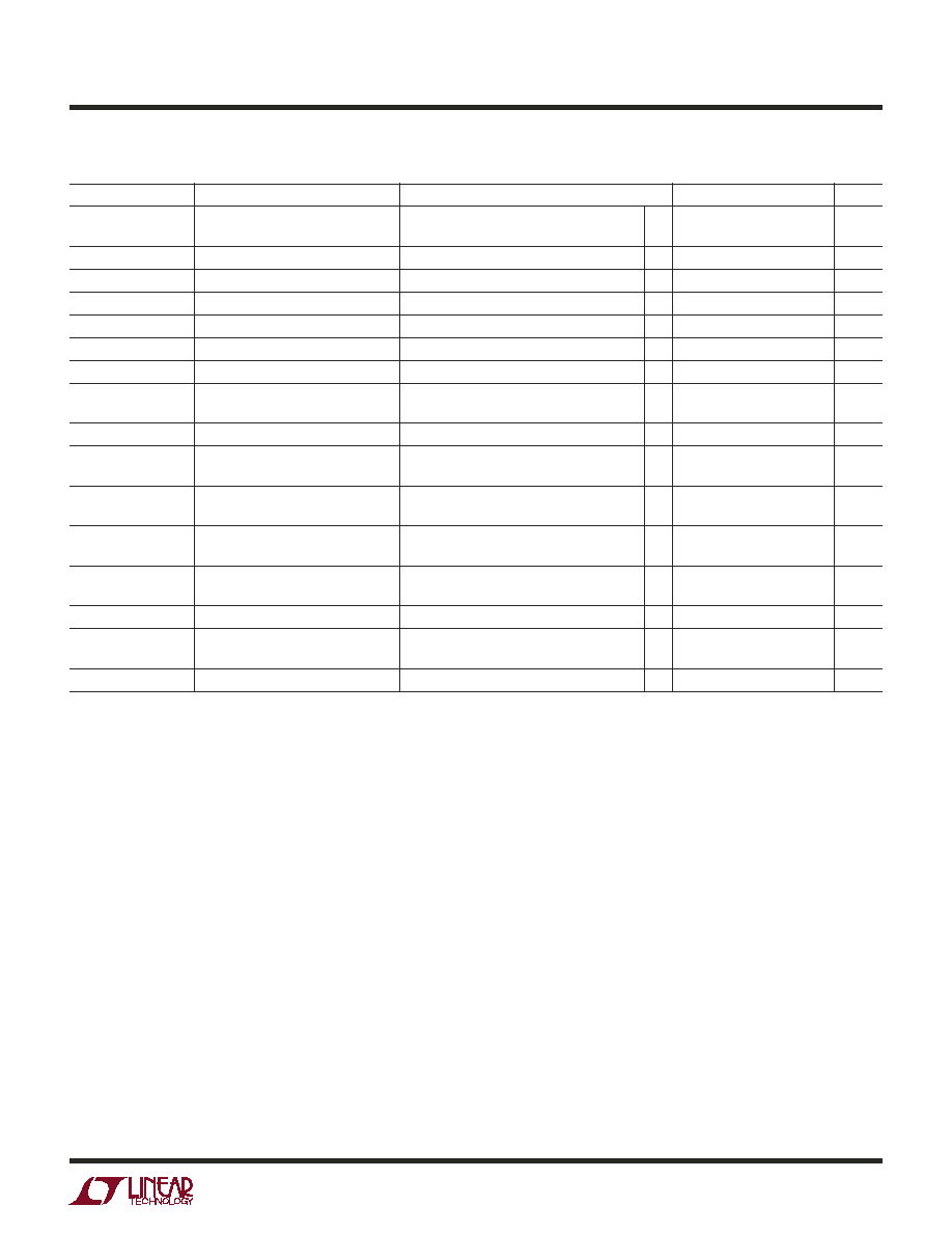
I
CC
vs V
CC
I
CC
vs Temperature
V
CC(UVLR)
vs Temperature
Normalized V
CB
vs V
CC
Normalized V
CB
vs Temperature
Normalized V
CB(FAST)
vs V
CC
Normalized V
CB(FAST)
vs
Temperature
I
GATE(UP)
vs V
CC
I
GATE(UP)
vs Temperature
TYPICAL PERFOR A CE CHARACTERISTICS
U
W
Specifications are at T
A
= 25∞C. V
CC
= 5V
unless otherwise noted.
BIAS SUPPLY VOLTAGE (V)
2.0
0
BIAS SUPPLY CURRENT (mA)
0.5
1.0
1.5
2.0
3.0
4.0
5.0
6.0
4213 G01
2.5
3.0
2.5
3.5
4.5
5.5
TEMPERATURE (∞C)
≠50
0
BIAS SUPPLY CURRENT (mA)
0.5
1.0
1.5
2.0
0
50
100
125
4213 G02
2.5
3.0
≠25
25
75
TEMPERATURE (∞C)
≠50
1.7
UNDERVOLTAGE LOCKOUT THRESHOLD (V)
1.8
1.9
2.0
2.1
0
50
100
125
4213 G03
2.2
2.3
≠25
25
75
V
CC
RISING
V
CC
FALLING
BIAS SUPPLY VOLTAGE (V)
2.0
0.94
NORMALIZED V
CB
0.96
0.98
1.00
1.02
3.0
4.0
5.0
6.0
4213 G04
1.04
1.06
2.5
3.5
4.5
5.5
TEMPERATURE (∞C)
≠50
0
50
100
125
4213 G05
≠25
25
75
0.94
NORMALIZED V
CB
0.96
0.98
1.00
1.02
1.04
1.06
BIAS SUPPLY VOLTAGE (V)
2.0
3.0
4.0
5.0
6.0
4213 G06
2.5
3.5
4.5
5.5
0.94
NORMALIZED V
CB(FAST)
0.96
0.98
1.00
1.02
1.04
1.06
TEMPERATURE (∞C)
≠50
0
50
100
125
4213 G07
≠25
25
75
0.94
NORMALIZED V
CB(FAST)
0.96
0.98
1.00
1.02
1.04
1.06
BIAS SUPPLY VOLTAGE (V)
2.0
96
I
GATE(UP)
(
µ
A)
98
100
102
3.0
4.0
5.0
6.0
4213 G08
104
2.5
3.5
4.5
5.5
TEMPERATURE (∞C)
≠50
0
50
100
125
≠25
25
75
96
I
GATE(UP)
(
µ
A)
98
100
102
4213 G09
104
LTC4213
5
4213f
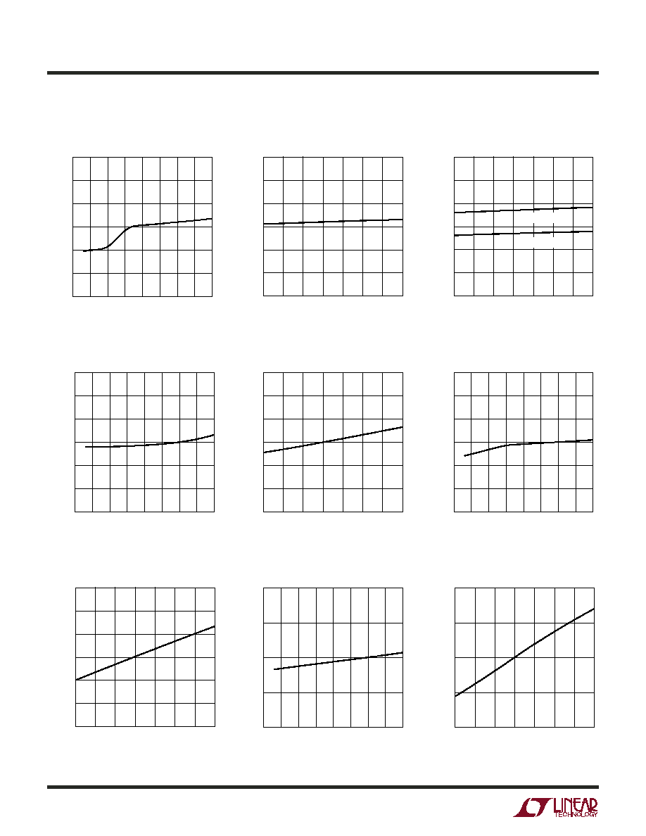
TYPICAL PERFOR A CE CHARACTERISTICS
U
W
V
GSMAX
and V
GSARM
vs V
CC
V
GSMAX
and V
GSARM
vs
Temperature
V
ON(TH)
vs V
CC
V
ON(TH)
vs Temperature
V
OV
vs V
CC
V
OV
vs Temperature
t
DEBOUNCE
and t
READY
vs V
CC
t
DEBOUNCE
and t
READY
vs
Temperature
t
RESET
vs V
CC
Specifications are at T
A
= 25∞C. V
CC
= 5V
unless otherwise noted.
BIAS SUPPLY VOLTAGE (V)
2.0
3
V
GSMAX
AND
V
GSARM
(V)
5
4
6
7
3.0
4.0
5.0
6.0
4213 G10
8
2.5
3.5
4.5
5.5
V
GSMAX
V
GSARM
3
V
GSMAX
AND
V
GSARM
(V)
5
4
6
7
4213 G11
8
TEMPERATURE (∞C)
≠50
0
50
100
125
≠25
25
75
V
GSMAX
(FOR 2.5V
CC
)
V
GSARM
(FOR 2.5V
CC
)
V
GSMAX
(FOR 5V
CC
)
V
GSARM
(FOR 5V
CC
)
BIAS SUPPLY VOLTAGE (V)
2.0
3.0
4.0
5.0
6.0
4213 G12
2.5
3.5
4.5
5.5
0.65
0.70
ON PIN THRESHOLD (V)
0.75
0.80
0.85
0.90
LOW THRESHOLD
HIGH THRESHOLD
BIAS SUPPLY VOLTAGE (V)
2.0
t
DEBOUNCE
AND t
READY
(
µ
s)
3.0
4.0
5.0
6.0
2.5
3.5
4.5
5.5
0
20
40
60
4213 G16
80
100
t
DEBOUNCE
t
READY
BIAS SUPPLY VOLTAGE (V)
2.0
0
t
RESET
(
µ
s)
40
20
60
80
3.0
4.0
5.0
6.0
4213 G18
100
120
2.5
3.5
4.5
5.5
TEMPERATURE (∞C)
≠50
0
50
100
125
4213 G13
≠25
25
75
0.65
0.70
ON PIN THRESHOLD (V)
0.75
0.80
0.85
0.90
LOW THRESHOLD
HIGH THRESHOLD
BIAS SUPPLY VOLTAGE (V)
2.0
3.0
4.0
5.0
6.0
4213 G14
2.5
3.5
4.5
5.5
0.66
OVERVOLTAGE THRESHOLD (V)
0.68
0.70
0.72
0.74
4213 G15
0.4
0.6
0.5
OVERVOLTAGE THRESHOLD (V)
0.7
0.8
0.9
1.0
TEMPERATURE (∞C)
≠50
0
50
100
125
≠25
25
75
TEMPERATURE (∞C)
≠50
0
50
100
125
≠25
25
75
t
DEBOUNCE
AND t
READY
(
µ
s)
0
20
40
60
4213 G17
80
100
t
DEBOUNCE
t
READY
LTC4213
6
4213f
t
RESET
vs Temperature
t
FAULT(SLOW)
vs V
CC
t
FAULT(SLOW)
vs Temperature
t
FAULT(FAST)
vs V
CC
t
FAULT(FAST)
vs Temperature
TYPICAL PERFOR A CE CHARACTERISTICS
U
W
Specifications are at T
A
= 25∞C. V
CC
= 5V
unless otherwise noted.
t
FAULT(FAST)
(
µ
s)
4213 G23
0.9
0.8
0.7
1.0
1.1
1.2
1.3
TEMPERATURE (∞C)
≠50
0
50
100
125
≠25
25
75
BIAS SUPPLY VOLTAGE (V)
2.0
10
t
FAULT(SLOW)
(
µ
s)
14
12
16
18
3.0
4.0
5.0
6.0
4213 G20
20
22
2.5
3.5
4.5
5.5
TEMPERATURE (∞C)
≠50
0
50
100
125
4213 G21
≠25
25
75
10
t
FAULT(SLOW)
(
µ
s)
14
12
16
18
20
22
TEMPERATURE (∞C)
≠50
0
50
100
125
4213 G19
≠25
25
75
t
RESET
(
µ
s)
60
70
80
90
100
BIAS SUPPLY VOLTAGE (V)
2.0
t
FAULT(FAST)
(
µ
s)
3.0
4.0
5.0
6.0
4213 G22
2.5
3.5
4.5
5.5
0.9
0.8
0.7
1.0
1.1
1.2
1.3

LTC4213
7
4213f
PI FU CTIO S
U
U
U
READY (Pin 1): READY Status Output. Open drain output
that goes high impedance when the external MOSFET is on
and the circuit breaker is armed. Otherwise this pin pulls
low.
ON
(Pin 2): ON Control Input. The LTC4213 is in reset
mode when the ON pin is below 0.4V. When the ON pin
increases above 0.8V, the device starts up and the GATE
pulls up with a 100µA current source. When the ON pin
drops below 0.76V, the GATE pulls down. To reset a circuit
breaker fault, the ON pin must go below 0.4V.
I
SEL
(Pin 3): Threshold Select Input. With the I
SEL
pin
grounded, float or tied to V
CC
the V
CB
is set to 25mV, 50mV
or 100mV, respectively. The corresponding V
CB(FAST)
values are 100mV, 175mV and 325mV.
GND
(Pin 4): Device Ground.
GATE
(Pin 5): GATE Drive Output. An internal charge
pump supplies 100µA pull-up current to the gate of the
external N-channel MOSFET. Internal circuitry limits the
voltage between the GATE and SENSEN pins to a safe gate
drive voltage of less than 8V. When the circuit breaker
trips, the GATE pin abruptly pulls to GND.
SENSEN
(Pin 6): Circuit Breaker Negative Sense Input.
Connect this pin to the source of the external MOSFET.
During reset or fault mode, the SENSEN pin discharges the
output to ground with 280µA.
SENSEP
(Pin 7): Circuit Breaker Positive Sense Input.
Connect this pin to the drain of external N-channel MOSFET.
The circuit breaker trips when the voltage across SENSEP
and SENSEN exceeds V
CB
. The input common mode range
of the circuit breaker is from ground to V
CC
+ 0.2V when
V
CC
< 2.5V. For V
CC
2.5V, the input common mode range
is from ground to V
CC
+ 0.4V.
V
CC
(Pin 8): Bias Supply Voltage Input. Normal operation
is between 2.3V and 6V. An internal under-voltage lockout
circuit disables the device when V
CC
< 2.07V.
Exposed Pad (Pin 9): Exposed pad may be left open or
connected to device ground.
LTC4213
8
4213f
BLOCK DIAGRA
W
V
CC
V
CB
0.7V
V
CB(FAST)
4213 BD
I
SEL
READY
GATE
ON
GND
V
CC
SENSEN
SENSEP
4
2
7
6
8
5
3
1
≠
+
+
≠
+≠
SENSEN
GATEOFF
RESET
STARTUP
NORMAL MODE
GATE ON/OFF
6.5V
CLAMP
CIRCUIT
CHARGE
PUMP
V
CB
100mV
50mV
25mV
V
CB(FAST)
325mV
175mV
100mV
V
GSARM
ARM
COMP
≠
+
COMP1
ARM
0.4V
LOGIC
≠
+
SLOWCOMP
+
≠
UV COMP
V
CC
2.07V
+
≠
COMP2
0.8V
80µs
DELAY
16µs
DELAY
50µs
DELAY
60µs
DELAY
8µs 5µs
CB TRIPS
+
≠
≠
+
FASTCOMP
1µs
DELAY
CB TRIPS
BLANK
RESET OR
FAULT MODE
280µA
100µA
+
≠
≠
+
OVCOMP
65µs
DELAY
OV TRIPS
GATE ON
V
CC
DELAY
LTC4213
9
4213f
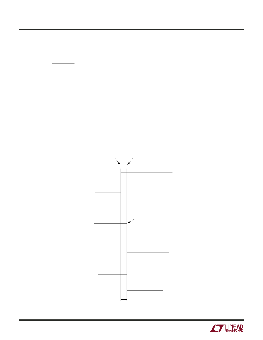
TI I G DIAGRA
W
U
W
0.3V
1.2V
0.3V
0.3V
V
ON(TH)
V
ON(RST)
1
2
3
4
5
6
1
2
3
4
5
V
ON
V
ON(TH)
V
ON(TH)
≠ V
ON(HYST)
V
ON(TH)
V
GSMAX
V
GSMAX
≠ 0.3V
V
GSMAX
V
GSMAX
≠ 0.3V
V
GATE
V
SENSE
V
ON
V
GATE
t
DEBOUNCE
t
OFF
t
ON
t
FAULT(FAST)
t
RESET
4213 TD
LTC4213
10
4213f
APPLICATIO S I FOR ATIO
W
U
U
U
Figure 1 shows an electronic circuit breaker (ECB) appli-
cation. An external auxiliary supply biases the V
CC
pin and
the internal circuitry. A V
IN
load supply powers the load via
an external MOSFET. The SENSEP and SENSEN pins
OPERATIO
U
Overview
The LTC4213 is an Electronic Circuit Breaker (ECB) that
senses load current with the the R
DSON
of the external
MOSFET instead of using an external sense resistor. This
no R
SENSE
method is less precise than R
SENSE
method due
to the variation of R
DSON
. However, the advantages are
less complex, lower cost and reduce voltage and power
loss in the switch path owing to the absence of a sense
resistor. Without the external sense resistor voltage drop,
the V
OUT
improvement can be quite significant especially
in the low voltage applications. The LTC4213 is designed
to operate over a bias supply range from 2.3V to 6V. When
bias supply voltage and the ON pin are sufficiently high, the
GATE pin starts charging after an internal debounce delay
of 60µs. During the GATE ramp-up, the circuit breaker is
not armed until the external MOSFET is fully turned on.
Once the circuit breaker is armed, the LTC4213 monitors
the load current through the R
DSON
of the external MOSFET.
Circuit Breaker Function
The LTC4213 provides dual level and dual response time
circuit breaker functions for overcurrent protection.
The LTC4213 circuit breaker function block consists of
two comparators, SLOWCOMP and FASTCOMP. The
thresholds of SLOWCOMP and FASTCOMP are V
CB
and
V
CB(FAST)
. The I
SEL
pin selects one of the three settings:
1. V
CB
= 25mV and V
CB(FAST)
= 100mV with I
SEL
at GND
2. V
CB
= 50mV and V
CB(FAST)
= 175mV with I
SEL
floating
3. V
CB
= 100mV and V
CB(FAST)
= 325mV with I
SEL
at V
CC
I
SEL
can be stepped dynamically, such as to allow a higher
circuit breaker threshold at startup and a lower threshold
after supply current has settled. The inputs of the com-
parators are SENSEP and SENSEN pins. The voltage
across the drain and source of the external MOSFET is
sensed at SENSEP and SENSEN.
V
V
V
SENSE
SENSEP
SENSEN
=
-
( )
1
When V
SENSE
exceeds the V
CB
threshold but is less than
V
CB(FAST)
, the comparator SLOWCOMP trips the circuit
breaker after a 16µs delay. If V
SENSE
is greater than
V
CB(FAST)
, the comparator FASTCOMP trips the circuit
breaker in 1µs.
A severe short circuit condition can cause the load supply
to dip substantially. This does not pose a problem for the
LTC4213 as the input stages of the current limit compara-
tors are common mode to ground.
sense the load current at the drain and source of the
external MOSFET. In ECB applications, large input bypass
capacitors are usually recommended for good transient
performance.
Undervoltage Lockout
An internal undervoltage lockout (UVLO) circuit resets the
LTC4213 if the V
CC
supply is too low for normal operation.
The UVLO comparator (UVCOMP) has a low-to-high thresh-
old of 2.07V and 100mV of hysteresis. UVLO shares the
glitch filters for both low-to-high transition (startup) and
high-to-low transition (reset) with the ON pin compara-
tors. Above 2.07V bias supply voltage, the LTC4213 starts
if the ON pin conditions are met. Short, shallow bus bias
4213 F01
+
LTC4213
V
CC
ON
READY
C1
0.1µF
C
LOAD
100µF
R4
10k
I
SEL
GND
GATE
Q1
SI4864DY
V
CC
V
OUT
1.25V
3.5A
SENSEN
SENSEP
V
BIAS
2.5V
V
IN
1.25V
+
C
IN
100µF
OFF ON
Figure 1. LTC4213 Electronic Circuit Breaker Application

LTC4213
11
4213f
supply transient dips below 1.97V of less than 80µs are
ignored.
ON Function
When V
ON
is below comparator COMP1's threshold of
0.4V for 80µs, the device resets. The system leaves reset
mode if the ON pin rises above comparator COMP2's
threshold of 0.8V and the UVLO condition is met. Leaving
reset mode, the GATE pin starts up after a t
DEBOUNCE
delay
of 60µs. When ON goes below 0.76V, the GATE shuts off
after a 5µs glitch filter delay. The output is discharged by
the external load when V
ON
is in between 0.4V to 0.8V. At
this state, the ON pin can re-enable the GATE if V
ON
exceeds 0.8V for more than 8µs. Alternatively, the device
resets if the ON pin is brought below 0.4V for 80µs. Once
reset, the GATE pin restarts only after the t
DEBOUNCE
60µs
delay at V
ON
rising above 0.8V. To protect the ON pin from
overvoltage stress due to supply transients, a series
resistor of greater than 10k is recommended when the ON
pin is connected directly to the supply. An external resis-
tive divider at the ON pin can be used with COMP2 to set
a supply undervoltage lockout value higher than the inter-
nal UVLO circuit. An RC filter can be implemented at the
ON pin to increase the powerup delay time beyond the
internal 60µs delay.
Gate Function
The GATE pin is held low in reset mode. 60µs after leaving
reset mode, the GATE pin is charged up by an internal
100µA current source. The circuit breaker arms when
V
GATE
> V
SENSEN
+ V
GSARM
. In normal mode operation,
the GATE peak voltage is internally clamped to V
GSMAX
above the SENSEN pin. When the circuit breaker trips, an
internal MOSFET shorts the GATE pin to GND, turning off
the external MOSFET.
READY Status
The READY pin is held low during reset and at startup. It
is pulled high by an external pullup resistor 50µs after the
circuit breaker arms. The READY pin pulls low if the circuit
breaker trips or the ON pin is pulled below 0.76V, or V
CC
drops below undervoltage lockout.
V
GSARM
and V
GSMAX
Each MOSFET has a recommended V
GS
drive voltage
where the channel is deemed fully enhanced and R
DSON
is
minimized. Driving beyond this recommended V
GS
volt-
age yields a marginal decrease in R
DSON
. At startup, the
gate voltage starts at ground potential. The GATE ramps
past the MOSFET threshold and the load current begins to
flow. When V
GS
exceeds V
GSARM
, the circuit breaker is
armed and enabled. The chosen MOSFET should have a
recommended minimum V
GS
drive level that is lower than
V
GSARM
. Finally, V
GS
reaches a maximum at V
GSMAX.
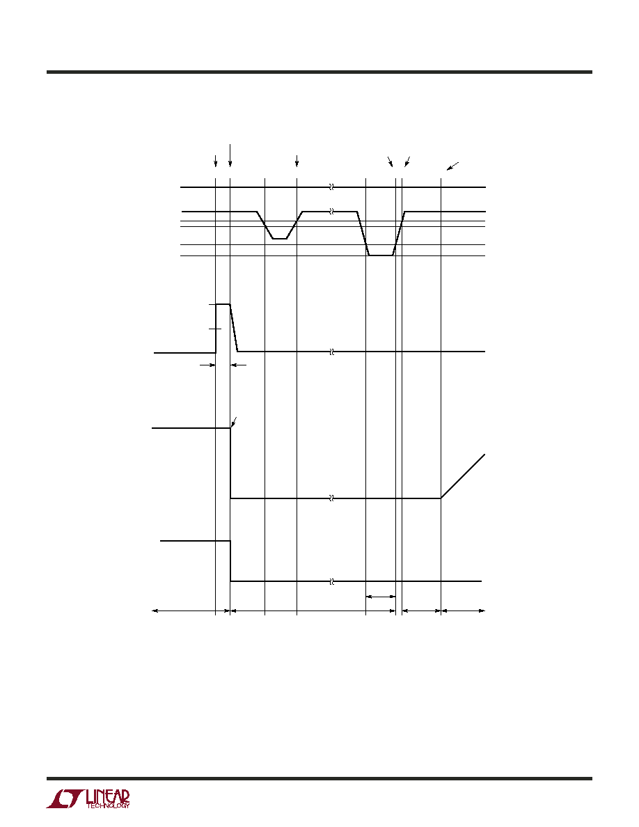
Trip and Reset Circuit Breaker
Figure 2 shows the timing diagram of V
GATE
and V
READY
after a fault condition. A tripped circuit breaker can be reset
either by cycling the V
CC
bias supply below UVLO thresh-
old or pulling ON below 0.4V for >t
RESET
. Figure 3 shows
the timing diagram for a tripped circuit breaker being reset
by the ON pin.
Calculating Current Limit
The fault current limit is determined by the R
DSON
of the
MOSFET and the circuit breaker voltage V
CB
.
I
V
R
LIMIT
CB
DSON
=
( )
2
The R
DSON
value depends on the manufacturer's distribu-
tion, V
GS
and junction temperature. Short Kelvin-sense
connections between the MOSFET drain and source to
the LTC4213 SENSEP and SENSEN pins are strongly
recommended.
For a selected MOSFET, the nominal load limit current is
given by:
I
V
R
LIMIT NOM
CB NOM
DSON NOM
(
)
(
)
(
)
( )
=
3
The minimum load limit current is given by:
I
V
R
LIMIT MIN
CB MIN
DSON MAX
(
)
(
)
(
)
( )
=
4
APPLICATIO S I FOR ATIO
W
U
U
U
LTC4213
12
4213f
APPLICATIO S I FOR ATIO
W
U
U
U
Figure 2. Short Circuit Fault Timing Diagram
A
B
CB TRIPS
V
SENSE
V
GATE
V
CB
>V
CB
V
READY
CIRCUIT BREAKER TRIPS
GATE AND READY PINS PULL LOW
SHORT CIRCUIT
t
FAULT
4213 F02
The maximum load limit current is given by:
I
V
R
LIMIT MAX
CB MAX
DSON MIN
(
)
(
)
(
)
( )
=
5
Most MOSFET data sheets have an R
DSON
specification
with typical and maximum values but no minimum value.
Assuming a normal distribution with typical as mean, the
minimum value can be estimated as
R
R
R
DSON MIN
DSON NOM
DSON MAX
(
)
(
)
(
)
( )
= ∑
-
2
6
The LTC4213 gives higher gate drive than the manufac-
turer specified gate drive for R
DSON
. This gives a slightly
lower R
DSON
than specified. Operating temperature also
modulates the R
DSON
value.
Example Current Limit Calculation
An Si4410DY is used for current detection in a 5V supply
system with the LTC4213 V
CB
at 25mV (I
SEL
pin grounded).
The R
DSON
distribution for the Si4410DY is
Typical R
DSON
= 0.015 = 100%
Maximum R
DSON
= 0.02 = 133.3%
Estimated MIN R
DSON
= 2 ∑ 15 ≠ 20 = 0.010 = 66.7%
The R
DSON
variation due to gate drive is
R
DSON
@ 4.5V
GS
= 0.015 = 100% (spec. TYP)
R
DSON
@ 4.8V
GS
= 0.014 = 93% (MIN V
GSMAX
)
R
DSON
@ 7V
GS
= 0.0123 = 82% (NOM V
GSMAX
)
R
DSON
@ 8V
GS
= 0.012 = 80% (MAX V
GSMAX
)
LTC4213
13
4213f
APPLICATIO S I FOR ATIO
W
U
U
U
Figure 3. Resetting Fault Timing Diagram
V
CB
1
2
3
4
5
6 7
8
RESTART
V
READY
V
GATE
NORMAL MODE
STARTUP CYCLE
V
ON
< 0.4V
DURATION > t
RESET
t
FAULT
t
DEBOUNCE
FAULT LATCHED OFF
V
CC
> 2.07V
V
SENSE
4213 F03
CIRCUIT BREAKER TRIPS
GATE AND READY PINS PULL LOW
SHORT CIRCUIT
NOT RESET
RESET REINITIALIZE
CB TRIPS
0V
V
ON
0.4V
0.76V
0.8V
>V
CB
LTC4213
14
4213f
Operating temperature of 0∞ to 70∞C.
R
DSON
@ 25∞C = 100%
R
DSON
@ 0∞C = 90%
R
DSON
@ 70∞C = 120%
MOSFET resistance variation:
R
DSON(NOM)
= 15m ∑ 0.82 = 12.3m
R
DSON(MAX)
= 15m ∑ 1.333 ∑ 0.93 ∑ 1.2 = 15m ∑ 1.488
= 22.3m
R
DSON(MIN)
= 15m ∑ 0.667 ∑ 0.80 ∑ 0.90 = 15m ∑ 0.480
= 7.2m
V
CB
variation:
NOM V
CB
= 25mV = 100%
MIN V
CB
= 22.5mV = 90%
MAX V
CB
= 27.5mV = 110%
The current limits are:
I
LIMIT(NOM)
= 25mV/12.3m = 2.03A
I
LIMIT(MIN)
= 22.5mV/22.3m = 1.01A
I
LIMIT(MAX)
= 27.5mV/7.2m = 3.82A
For proper operation, the minimum current limit must
exceed the circuit maximum operating load current with
margin. So this system is suitable for operating load
current up to 1A. From this calculation, we can start with
the general rule for MOSFET R
DSON
by assuming maxi-
mum operating load current is roughly half of the
I
LIMIT(NOM)
. Equation 7 shows the rule of thumb.
I
V
R
OPMAX
CB NOM
DSON NOM
=
(
)
(
)
∑
( )
2
7
Note that the R
DSON(NOM)
is at the LTC4213 nominal
operating V
GSMAX
rather than at typical vendor spec.
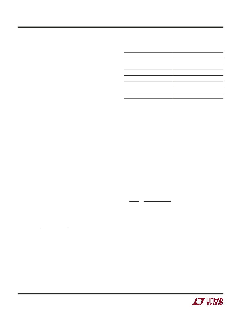
Table 1 gives the nominal operating V
GSMAX
at the
various operating V
CC
. From this table users can refer to
the MOSFET's data sheet to obtain the R
DSON(NOM)
value.
Table 1. Nominal Operating V
GSMAX
for Typical Bias
Supply Voltage
V
CC
(V)
V
GSMAX
(V)
2.3
4.3
2.5
5.0
2.7
5.6
3.0
6.5
3.3
7.0
5.0
7.0
6.0
7.0
Load Supply Power-Up after Circuit Breaker Armed
Figure 4 shows a normal power-up sequence for the
circuit in Figure 1 where the V
IN
load supply power-up after
circuit breaker is armed. V
CC
is first powered up by an
auxiliary bias supply. V
CC
rises above 2.07V at time
point 1. V
ON
exceeds 0.8V at time point 2. After a 60µs
debounce delay, the GATE pin starts ramping up at time
point 3. The external MOSFET starts conducting at time
point 4. At time point 5, V
GATE
exceed V
GSARM
and the
circuit breaker is armed. After 50µs (t
READY
delay), READY
pulls high by an external resistor at time point 6. READY
signals the V
IN
load supply module to start its ramp. The
load supply begins soft-start ramp at time point 7. The load
supply ramp rate must be slow to prevent circuit breaker
tripping as in equation (8).
V
t
I
I
C
IN
OPMAX
LOAD
LOAD
<
-
( )
8
Where I
OPMAX
is the maximum operating current defined
by equation 7.
For illustration, V
CB
= 25mV and R
DSON
= 3.5m at the
nominal operating V
GSMAX
. The maximum operating
current is 3.5A (refer to equation 7). Assuming the load
can draw a current of 2A at power-up, there is a margin of
1.5A available for C
LOAD
of 100µF and V
IN
ramp rate should
be <15V/ms. At time point 8, the current through the
MOSFET reduces after C
LOAD
is fully charged.
APPLICATIO S I FOR ATIO
W
U
U
U
LTC4213
15
4213f
APPLICATIO S I FOR ATIO
W
U
U
U
Figure 4. Load Supply Power-Up After Circuit Breaker Armed
0.8V
2.07V
100µA
1
2
3
4
5
6 7
8
V
CC
, V
ON
CIRCUIT BREAKER ARMS
V
th
V
GSMAX
V
GSMAX
+ V
SENSEN
V
GSARM
V
CB
V
READY
V
GATE
V
SENSE
RESET MODE
NORMAL CYCLE
t
READY
STARTUP CYCLE
t
DEBOUNCE
V
SENSEP
, V
SENSEN
4213 F04
LTC4213
16
4213f
APPLICATIO S I FOR ATIO
W
U
U
U
Figure 5. Load Supply Power-Up Before V
CC
V
ON
> 0.8V
V
th
0
1
2
3
4
5
6
7
8
V
CC
, V
ON
CIRCUIT BREAKER ARMS
READY SIGNALS
V
READY
V
SENSEN
V
SENSEP
RESET MODE
NORMAL CYCLE
t
READY
STARTUP CYCLE
t
DEBOUNCE
V
GATE
4213 F05
V
SENSEP
≠ V
SENSEN
= V
CB
V
GATE
MAXES OUT
V
CC
> 2.07V
V
GSARM
+ V
SENSEN
V
GSMAX
+ V
SENSEN
Load Supply Power-Up Before V
CC
Referring back to Figure 1, the V
IN
load supply can also be
powered up before V
CC
. Figure 5 shows the timing dia-
gram with the V
IN
load supply active initially. An internal
circuit ensures that the GATE pin is held low. At time point
1, V
CC
clears UVLO and at time point 2, ON clears 0.8V.
60µs later at time point 3, the GATE is ramped up with
100µA. At time point 4, GATE reaches the external MOSFET
threshold V
TH
and V
OUT
starts to ramp up. At time point 5,
V
SENSEN
is near its peak. At time point 6, the circuit breaker
is armed and the circuit breaker can trip if V
SENSE
> V
CB
.
At time point 7, the GATE voltage peaks. 50µs after time
point 6, READY goes HIGH.
Startup Problems
There is no current limit monitoring during output charg-
ing for the figure 5 power-up sequence where the load
supply is powered up before V
CC
. This is because the GATE
voltage is below V
GSARM
and the MOSFET may not reach
the specified R
DSON
. The V
IN
load supply should have
sufficient capability to handle the inrush as the output
charges up. For proper startup, the final load at time

LTC4213
17
4213f
The selected MOSFET V
GS
absolute maximum rating should
meet the LTC4213 maximum V
GSMAX
of 8V.
Other MOSFET criteria such as V
BDSS
, I
DMAX
, and R
DSON
should be reviewed. Spikes and ringing above maximum
operating voltage should be considered when choosing
V
BDSS
. I
DMAX
should be greater than the current limit. The
maximum operating load current is determined by the
R
DSON
value. See the section on "Calculating Current
Limit" for details.
Supply Requirements
The LTC4213 can be powered from a single supply or dual
supply system. The load supply is connected to the
SENSEP pin and the drain of the external MOSFET. In the
single supply case, the V
CC
pin is connected to the load
supply, preferably with an RC filter. With dual supplies,
V
CC
is connected to an auxiliary bias supply V
AUX
where
V
AUX
voltage should be greater or equal to the load supply
voltage. The load supply voltage must be capable of
sourcing more current than the circuit breaker limit. If the
load supply current limit is below the circuit breaker trip
current, the LTC4213 may not react when the output
overloads. Furthermore, output overloads may trigger
UVLO if the load supply has foldback current limit in a
single supply system.
V
IN
Transient and Overvoltage Protection
Input transient spikes are commonly observed whenever
the LTC4213 responds to overload. These spikes can be
large in amplitude, especially given that large decoupling
capacitors are absent in hot swap environments. These
short spikes can be clipped with a transient suppressor of
adequate voltage and power rating. In addition, the LTC4213
can detect a prolonged overvoltage condition. When
APPLICATIO S I FOR ATIO
W
U
U
U
point 6 should be within the circuit breaker limits. Other-
wise, the system fails to start and the circuit breaker trips
immediately after arming. In most applications additional
external gate capacitance is not required unless C
LOAD
is
large and startup becomes problematic. If an external gate
capacitor is employed, its capacitance value should not be
excessive unless it is used with a series resistor. This is
because a big gate capacitor without resistor slows down
the GATE turn off during a fault. An alternative method
would be a stepped I
SEL
pin to allow a higher current limit
during startup.
In the event of output short circuit or a severe overload, the
load supply can collapse during GATE ramp up due to load
supply current limit. The chosen MOSFET must withstand
this possible brief short circuit condition before time
point 6 where the circuit breaker is allowed to trip. Bench
short circuit evaluation is a practical verification of a
reliable design. To have current limit while powering a
MOSFET into short circuit conditions, it is preferred that
the load supply sequences to turn on after the circuit
breaker is armed as described in an earlier section.
Power-Off Cycle
The system can be powered off by toggling the ON pin low.
When ON is brought below 0.76V for 5µs, the GATE and
READY pins are pulled low. The system resets when ON is
brought below 0.4V for 80µs.
MOSFET Selection
The LTC4213 is designed to be used with logic (5V) and
sub-logic (3V) MOSFETs for V
CC
potentials above 2.97V
with V
GSMAX
exceeding 4.5V. For a V
CC
supply range
between 2.3V and 2.97V, sub-logic MOSFETs should be
used as the minimum V
GSMAX
is less than 4.5V.
LTC4213
18
4213f
APPLICATIO S I FOR ATIO
W
U
U
U
4213 F06
+
LTC4213
V
CC
ON
READY
C1
10µF
C
LOAD
100µF
R4
10k
I
SEL
GND
GATE
Q1
SI4410DY
Q2
2N7002
V
IN
V
OUT
5V
1A
SENSEN
SENSEP
C
IN
100µF
R1
33
D1
MBRO520L
R3
324k
R2
80.6k
RESET
V
IN
5V
+
C2
0.22µF
Figure 6. Single Supply Electronic Fuse
SENSEP exceeds V
CC
+ 0.7V for more than 65µs, the
LTC4213's internal overvoltage protection circuit acti-
vates and the GATE pin pulls down and turns off the
external MOSFET.
Typical Electronic Fuse Application for a Single
Supply System
Figure 6 shows a single supply electronic fuse application.
An RC filter at V
CC
pin filters out transient spikes. An
optional Schottky diode can be added if severe V
CC
dips
during a fault start-up condition is a concern. The use of
the Schottky and RC filter combination is allowed if the
load supply is above 2.9V and the total voltage drop
towards the V
CC
pin is less than 0.4V. The LTC4213's
internal UVLO filter further rejects bias supply's transients
of less than t
RESET
. During power-up, it is good engineer-
ing practice to ensure that V
CC
is fully established before
the ON pin enables the system at V
ON
= 0.8V. In this
application, the V
CC
voltage reached final value approxi-
mately after a 5.3 ∑ R
1
C
1
delay. This is followed by the ON
pin exceeding 0.8V after a 0.17 ∑ R
2
C
2
delay. The GATE pin
starts up after an internal t
DEBOUNCE
delay.
Hot Swap is a trademark of Linear Technology Corporation.
Typical Single Supply Hot SwapTM Application
A typical single supply Hot Swap application is shown in
Figure 7. The RESET signal at the backplane is held low
initially. When the PCB long edge makes contact the ON
pin is held low (<0.4V) and the LTC4213 is kept in reset
mode. When the short edge makes contact the V
IN
load
supply is connected to the card. The V
CC
is biased via the
RC filter. The V
OUT
is pre-charged via R5. To power-up
successfully, the R5 resistor value should be small enough
to provide the load requirement and to overcome the
280µA current source sinking into the SENSEN pin. On the
other hand, the R5 resistor value should be big enough
avoiding big inrush current and preventing big short
circuit current. When RESET signals high at backplane, C2
capacitor at the ON pin charges up via the R3/R2 resistive
divider. When ON pin voltage exceeds 0.8V, the GATE pin
begins to ramp up. When the GATE voltage peaks, the
external MOSFET is fully turned on and the V
IN
-to-V
OUT
voltage drop reduces. In normal mode operation, the
LTC4213 monitors the load current through the R
DSON
of
the external MOSFET.
LTC4213
19
4213f
PACKAGE DESCRIPTIO
U
Information furnished by Linear Technology Corporation is believed to be accurate and reliable.
However, no responsibility is assumed for its use. Linear Technology Corporation makes no represen-
tation that the interconnection of its circuits as described herein will not infringe on existing patent rights.
2.00 ±0.10
(2 SIDES)
NOTE:
1. DRAWING CONFORMS TO VERSION (WECD-1) IN JEDEC PACKAGE OUTLINE M0-229
2. DRAWING NOT TO SCALE
3. ALL DIMENSIONS ARE IN MILLIMETERS
4. DIMENSIONS OF EXPOSED PAD ON BOTTOM OF PACKAGE DO NOT INCLUDE
MOLD FLASH. MOLD FLASH, IF PRESENT, SHALL NOT EXCEED 0.15mm ON ANY SIDE
5. EXPOSED PAD SHALL BE SOLDER PLATED
6. SHADED AREA IS ONLY A REFERENCE FOR PIN 1 LOCATION ON THE TOP AND BOTTOM OF PACKAGE
0.38 ± 0.10
BOTTOM VIEW--EXPOSED PAD
0.56 ± 0.05
(2 SIDES)
0.75 ±0.05
R = 0.115
TYP
2.15 ±0.05
(2 SIDES)
3.00 ±0.10
(2 SIDES)
1
4
8
5
PIN 1 BAR
TOP MARK
(SEE NOTE 6)
0.200 REF
0 ≠ 0.05
(DDB8) DFN 1103
0.25 ± 0.05
2.20 ±0.05
(2 SIDES)
RECOMMENDED SOLDER PAD PITCH AND DIMENSIONS
0.61 ±0.05
(2 SIDES)
1.15 ±0.05
0.675 ±0.05
2.50 ±0.05
PACKAGE
OUTLINE
0.25 ± 0.05
0.50 BSC
PIN 1
CHAMFER OF
EXPOSED PAD
0.50 BSC
DDB Package
8-Lead Plastic DFN (3mm ◊ 2mm)
(Reference LTC DWG # 05-08-1702)

LTC4213
20
4213f
Linear Technology Corporation
1630 McCarthy Blvd., Milpitas, CA 95035-7417
(408) 432-1900
FAX: (408) 434-0507
www.linear.com
© LINEAR TECHNOLOGY CORPORATION 2005
LT/TP 0405 500 ∑ PRINTED IN USA
RELATED PARTS
TYPICAL APPLICATIO
U
4213 TA02
+
LTC4213
V
CC
ON
READY
C2
1µF
C
LOAD
100µF
R4
10k
R5
330
R3
182k
I
SEL
NC
GND
GATE
Q1
IRF7455
V
OUT
3.3V
3.6A
SENSEN
SENSEP
Zx
SMAJ6.0A
D1
BAT54ALT1
C1
2.2µF
R1
68
R2
80.6k
RESET
V
IN
3.3V
V
IN
BACKPLANE GND
CARD GND
STAGGERED
PCB EDGE
CONNECTOR
Figure 7. Single Supply Hot Board Insertion
PART NUMBER
DESCRIPTION
COMMENTS
LTC1421
Dual Channel, Hot SwapTM Controller
24-Pin, Operates from 3V to 12V and Supports ≠12V
LTC1422
Single Channel, Hot Swap Controller in SO-8
Operates from 2.7V to 12V, System Reset Output
LTC1642
Fault Protected, Hot Swap Controller
Operates up to 16.5V, Overvoltage Protection to 33V
LTC1643AL/LTC1643AH
PCI Hot Swap Controllers
3.3V, 5V and ±12V Supplies
LTC1645
Dual Channel Hot Swap Controller
Operates from 1.2V to 12V, Power Sequencing
LTC1647
Dual Channel, Hot Swap Controller
Operates from 2.7V to 16.5V
LTC4210
Single Channel, Hot Swap Controller in SOT-23
Operates from 2.7V to 16.5V, Multifunction Current Control
LTC4211
Single Channel, Hot Swap Controller in MSOP
2.5V to 16.5V, Multifunction Current Control
LTC4216
Ultra Low Voltage Hot Swap Controller
Operates from 2.7V to 16.5V, Multifunction Current
LTC4221
Dual Channel, Hot Swap Controller
Protects Load Voltages from 0V to 6V
LTC4230
Triple Channel, Hot Swap Controller
1.7V to 16.5V, Multifunction Current Control
LTC4251
≠48V Hot Swap Controller in S0T-23
≠48V Hot Swap Controller, Active Current Limiting
LTC4252
≠48V Hot Swap Controller in MSOP
Active Current Limiting with Drain Acceleration
LTC4253
≠48V Hot Swap Controller and Sequencer
Active Current Limiting with Drain Acceleration and Three
Sequenced Power Good Outputs