4215f.indd
LTC4215
1
4215f
Hot Swap Controller with
I
2
C Compatible Monitoring
Live Board Insertion
Electronic Circuit Breakers
Computers, Servers
Platform Management
Allows Safe Insertion into Live Backplane
8-Bit ADC Monitors Current and Voltage
I
2
C/SMBus Interface
Wide Operating Voltage Range: 2.9V to 15V
dI/dt Controlled Soft-Start
High Side Drive for External N-Channel MOSFET
No External Gate Capacitor Required
Input Overvoltage/Undervoltage Protection
Optional Latchoff or Auto-Retry After Faults
Alerts Host After Faults
Inrush Current Limit with Foldback
Available in 24-Lead (4mm
� 5mm) QFN and
16-Lead Narrow SSOP Packages
APPLICATIO S
U
FEATURES
DESCRIPTIO
U
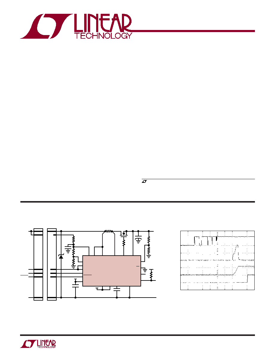
TYPICAL APPLICATIO
U
, LTC and LT are registered trademarks of Linear Technology Corporation.
Hot Swap is a trademark of Linear Technology Corporation.
All other trademarks are the property of their respective owners.
+
UV V
DD
SENSE
+
SENSE
�
LTC4215UFD
GATE
TIMER SS
ON
GND
SOURCE
OV
SDAO
SDAI
SCL
ALERT
INTV
CC
FB
EN
ADIN
GPIO
2.67k
PLUG-IN
CARD
1.74k
20V
10
0.005
FDC653N
30.1k
V
OUT
12V
3.57k
24k
4215 TA01a
C
L
0.1
�F
CONNECTOR 2
CONNECTOR 1
0.1
�F
34k
BACKPLANE
68nF
GND
ALERT
SCL
SDA
12V
The LTC
�
4215 Hot Swap
TM
controller allows a board to be
safely inserted and removed from a live backplane. Using
an external N-channel pass transistor, board supply voltage
and inrush current are ramped up at an adjustable rate.
An I
2
C interface and onboard ADC allow for monitoring
of load current, voltage and fault status.
The device features adjustable foldback current limit and
a soft-start pin that sets the dI/dt of the inrush current.
An I
2
C interface may confi gure the part to latch off or
automatically restart after the LTC4215 detects a current
limit fault.
The controller has additional features to interrupt the host
when a fault has occurred, notify when output power is
good, detect insertion of a load card, and power-up either
automatically upon insertion or wait for an I
2
C command
to turn on.
4215 TA01b
C
L
= 12000
�F
50ms/DIV
V
DD
10V/DIV
V
OUT
10V/DIV
V
GPIO
(POWERGOOD)
10V/DIV
INRUSH
CURRENT
2.5A/DIV
CONTACT
BOUNCE
LTC4215
2
4215f
Supply Voltage (V
DD
) ................................ �0.3V to 24V
Supply Voltage (INTV
CC
) .......................... �0.3V to 6.5V
Input Voltages
GATE-SOURCE (Note 3) .......................... �0.3V to 5V
SENSE
+
, SENSE
�
................ V
DD
� 0.3V to V
DD
+ 0.3V
SOURCE .................................................... �5V to 24V
EN, FB, ON, OV, UV ................................ �0.3V to 12V
ADR0, ADR1, ADR2, TIMER,
ADIN, SS ................................ �0.3V to INTV
CC
+ 0.3V
ALERT, SCL, SDA, SDAI, SDAO ............ �0.3V to 6.5V
(Notes 1, 2)
ABSOLUTE AXI U
RATI GS
W
W
W
U
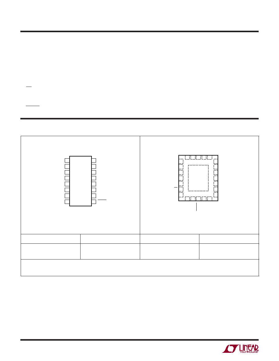
PACKAGE/ORDER I FOR ATIO
U
U
W
GN PACKAGE
16-LEAD PLASTIC TSSOP
1
2
3
4
5
6
7
8
TOP VIEW
16
15
14
13
12
11
10
9
SENSE
�
V
DD
UV
SS
GND
ON
SDA
SCL
GATE
SOURCE
FB
GPIO
INTV
CC
TIMER
ADR0
ALERT
T
JMAX
= 125�C,
JA
= 130�C/W
8
9
TOP VIEW
25
UFD PACKAGE
24-LEAD (4mm
� 5mm) PLASTIC QFN
10 11 12
24 23 22 21 20
6
5
4
3
2
1
UV
OV
SS
GND
ON
EN
SDAO
FB
GPIO
INTV
CC
TIMER
ADIN
ADR2
ADR1
V
DD
SENSE
+
SENSE
�
GATE
SOURCE
SDAI
ACL
ALERT
NC
ADR0
7
14
15
16
17
18
19
13
T
JMAX
= 125�C,
JA
= 43�C/W
EXPOSED PAD (PIN 25) NOT GUARANTEED LOW IMPEDANCE TO GND,
ELECTRICAL CONNECTION OPTIONAL
ORDER PART NUMBER
GN PART MARKING
ORDER PART NUMBER
UFD PART MARKING*
LTC4215CGN
LTC4215IGN
4215
4215I
LTC4215CUFD
LTC4215IUFD
4215
4215
Order Options Tape and Reel: Add #TR
Lead Free: Add #PBF Lead Free Tape and Reel: Add #TRPBF
Lead Free Part Marking:
http://www.linear.com/leadfree/
*The temperature grade is identifi ed by a label on the shipping container. Consult LTC Marketing for parts specifi ed with wider operating temperature ranges.
Output Voltages
GATE, GPIO ............................................ �0.3V to 24V
Operating Temperature Range
LTC4215C ................................................ 0�C to 70�C
LTC4215I ............................................. �40�C to 85�C
Storage Temperature Range
SSOP ................................................. �65�C to 150�C
QFN .................................................... �65�C to 125�C
Lead Temperature (Soldering, 10 sec)
SSOP
................................................................ 300�C
LTC4215
3
4215f
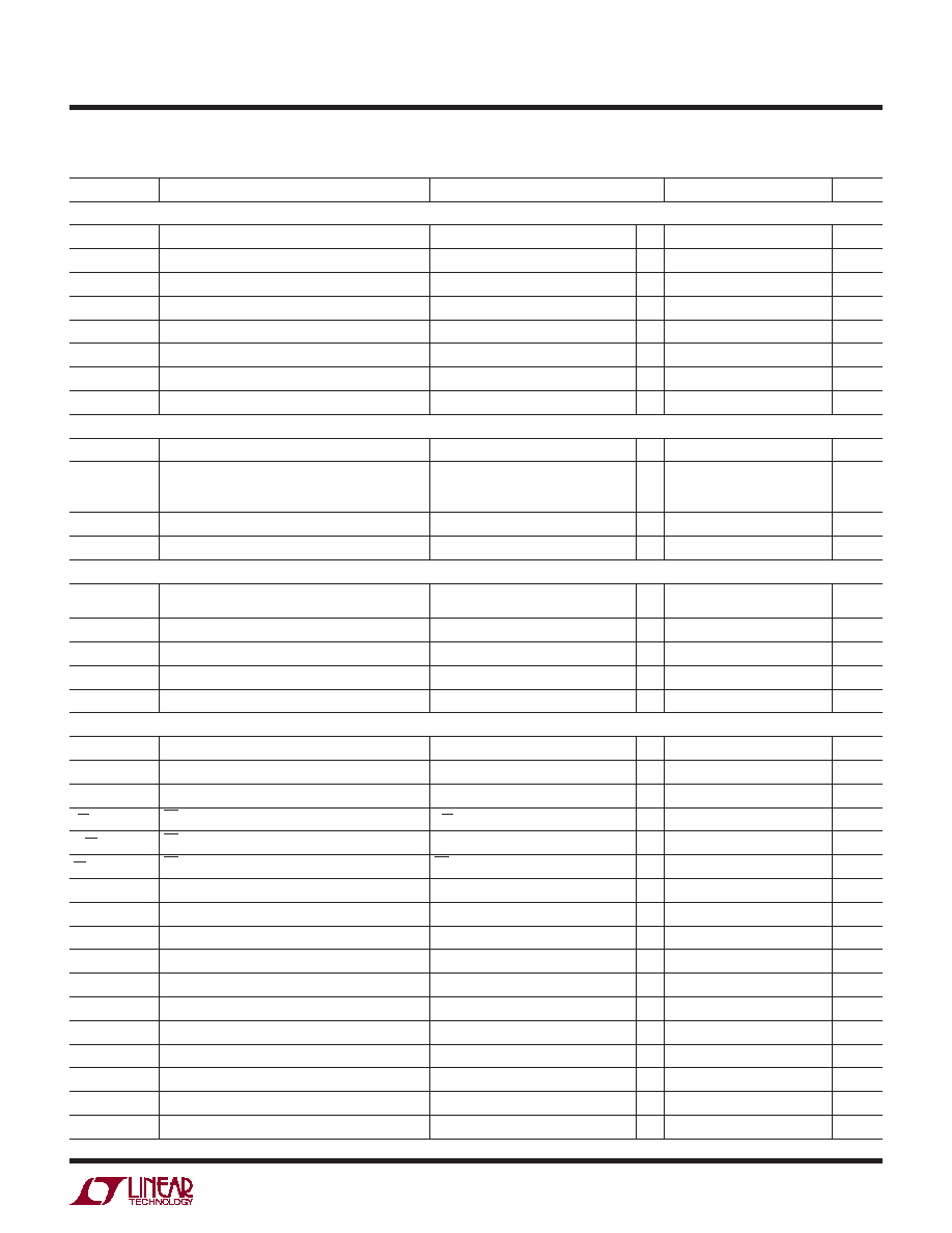
SYMBOL
PARAMETER
CONDITIONS
MIN
TYP
MAX
UNITS
Supplies
V
DD
Input Supply Range
2.9
15
V
V
OV(VDD)
Input Supply Overvoltage Threshold
15
15.6
16.5
V
I
DD
Input Supply Current
3
5
mA
V
DD(UVL)
Input Supply Undervoltage Lockout
V
DD
Rising
2.75
2.84
2.89
V
V
DD(HYST)
Input Supply Undervoltage Lockout Hysteresis
75
100
125
mV
INTV
CC
Internal Regulator Voltage
V
DD
3.3V
2.9
3.1
3.4
V
INTV
CC(UVL)
INTV
CC
Undervoltage Lockout
INTV
CC
Rising
2.55
2.64
2.79
V
INTV
CC(HYST)
INTV
CC
Undervoltage Lockout Hysteresis
20
55
75
mV
Current Limit and Circuit Breaker
V
SENSE(TH)
Circuit Breaker Threshold (V
DD
� V
SENSE
)
22.5
25
27.5
mV
V
SENSE
Current Limit Voltage (V
DD
� V
SENSE
)
V
FB
= 1.3V
V
FB
= 0V
Start-Up Timer Expired
22
6.5
65
25
10
75
29
13
90
mV
mV
mV
t
D(OC)
OC Fault Filter
V
SENSE
= 50mV
15
20
30
�s
I
SENSE(IN)
SENSE Pin Input Current
V
SENSE
= 12V
10
20
35
�A
Gate Drive
V
GATE
External N-Channel Gate Drive (V
GATE
� V
SOURCE
)
(Note 3)
V
DD
= 2.9V to 15V, I
GATE
= �1�A
5.0
5.9
6.5
V
I
GATE(UP)
External N-Channel Gate Pull-Up Current
Gate On, V
GATE
= 0V
�15
�20
�30
�A
I
GATE(DN)
External N-Channel Gate Pull-Down Current
Gate Off, V
GATE
= 15V
0.8
1
1.6
mA
t
PHL(SENSE)
(V
DD
� SENSE) High to GATE Low
V
DD
� SENSE = 100mV, C
GS
= 10nF
0.5
1
�s
V
GS(POWERBAD)
Gate-Source Voltage for Power Bad Fault
V
SOURCE
= 2.9V � 15V
3.8
4.3
5.0
V
Comparator Inputs
V
ON(TH)
ON Pin Threshold Voltage
V
ON
Rising
1.210
1.235
1.26
V
V
ON(HYST)
ON Pin Hysteresis
60
128
180
mV
I
ON(IN)
ON Pin Input Current
V
ON
= 1.2V
0
�1
�A
V
EN(TH)
EN Input Threshold
V
EN
= Rising
1.215
1.235
1.255
V
V
EN(HYST)
EN Hysteresis
50
128
200
mV
I
EN
EN Pin Input Current
EN = 3.5V
0
�1
�A
V
OV(TH)
OV Pin Threshold Voltage
V
OV
Rising
1.215
1.235
1.255
V
V
OV(HYST)
OV Pin Hysteresis
10
30
40
mV
I
OV(IN)
OV Pin Input Current
V
OV
= 1.8V
0
�1
�A
V
UV(TH)
UV Pin Threshold Voltage
V
UV
Rising
1.215
1.235
1.255
V
V
UV(HYST)
UV Pin Hysteresis
60
80
100
mV
I
UV(IN)
UV Pin Input Current
V
UV
= 1.8V
0
�1
�A
V
UV(RTH)
UV Pin Reset Threshold Voltage
V
UV
Falling
0.33
0.4
0.47
V
V
UV(RHYST)
UV Pin Reset Threshold Hysteresis
60
125
210
mV
V
FB
Foldback Pin Power Good Threshold
FB Rising
3
8
15
mV
V
FB(HYST)
FB Pin Power Good Hysteresis
3
8
13
mV
I
FB
Foldback Pin Input Current
FB = 1.8V
0
�1
�A
ELECTRICAL CHARACTERISTICS
The
denotes the specifi cations which apply over the full operating
temperature range, otherwise specifi cations are at T
A
= 25�C. V
DD
= 12V unless otherwise noted.
LTC4215
4
4215f
ELECTRICAL CHARACTERISTICS
The
denotes the specifi cations which apply over the full operating
temperature range, otherwise specifi cations are at T
A
= 25�C. V
DD
= 12V unless otherwise noted.
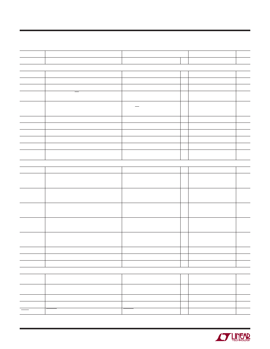
SYMBOL
PARAMETER
CONDITIONS
MIN
TYP
MAX
UNITS
V
GPIO(TH)
GPIO Pin Input Threshold
V
GPIO
Rising
0.8
1
1.2
V
Other Pin Functions
V
GPIO(OL)
GPIO Pin Output Low Voltage
I
GPIO
= 5mA
0.25
0.5
V
I
GPIO(OH)
GPIO Pin Input Leakage Current
V
GPIO
= 15V
0
�1
�A
I
SOURCE
SOURCE Pin Input Current
SOURCE = 15V
40
80
120
�A
t
P(GATE)
Input (ON, OV, UV, EN) to GATE Off
Propagation Delay
3
5
�s
t
D(GATE)
Turn-On Delay
ON
UV, OV, EN
Overcurrent Auto-Retry
50
2.5
1
100
5
2
150
75
�s
ms
s
V
TIMERL(TH)
Timer Low Threshold
0.17
0.2
0.23
V
V
TIMERH(TH)
Timer High Threshold
1.2
1.235
1.26
V
I
TIMER(UP)
TIMER Pin Pull-Up Current
�80
�100
�120
�A
I
TIMER(DOWN)
TIMER Pin Pull-Down Current for OC Auto-Retry
1.4
2
2.6
�A
I
TIMER(UP/DOWN)
TIMER Current Up/Down Ratio
40
50
60
�A
I
SS
Soft-Start Ramp Pull-Up Current
Ramping
Waiting for GATE to Slew
�7.5
�0.4
�10
�0.7
�12.5
�1.0
�A
�A
ADC
Resolution (No Missing Codes)
8
Bits
Integral Nonlinearity
V
DD
� SENSE (Note 5)
SOURCE
ADIN
�2
�1.25
�1.25
0.5
0.2
0.2
2
1.25
1.25
LSB
LSB
LSB
Offset Error (Note 4)
V
DD
� SENSE
SOURCE
ADIN
�2.0
�1.0
�1.0
LSB
LSB
LSB
Total Unadjusted Error
V
DD
� SENSE
SOURCE
ADIN
�5.5
�5.0
�5.0
LSB
LSB
LSB
Full-Scale Error
V
DD
� SENSE
SOURCE
ADIN
�5.5
�5.0
�5.0
LSB
LSB
LSB
Full-Scale Voltage (255 � V
LSB
)
V
DD
� SENSE
SOURCE
ADIN
37.625
15.14
1.205
38.45
15.44
1.23
39.275
15.74
1.255
mV
V
V
R
ADIN
ADIN Pin Sampling Resistance
V
ADIN
= 1.28V
1
2
M
I
ADIN
ADIN Pin Input Current
V
ADIN
= 1.28V
0
�0.1
�A
Conversion Rate
10
Hz
I
2
C Interface
V
ADR(H)
ADR0, ADR1, ADR2 Input High Voltage
INTV
CC
� 8
INTV
CC
� 0.4
INTV
CC
� 0.2
V
I
ADR(IN,Z)
ADR0, ADR1, ADR2 Hi-Z Input Current
ADR0, ADR1, ADR2 = 0.8V
ADR0, ADR1, ADR2 = INTV
CC
� 0.8V
3
�3
�A
�A
V
ADR(L)
ADR0, ADR1, ADR2 Input Low Voltage
0.2
0.4
0.8
V
I
ADR(IN)
ADR0, ADR1, ADR2 Input Current
ADR0, ADR1, ADR2 = 0V, INTV
CC
�80
80
�A
I
ALERT
ALERT Input Current
ALERT = 6.5V
�1
�A
LTC4215
5
4215f
Note 1: Stresses beyond those listed under Absolute Maximum Ratings
may cause permanent damage to the device. Exposure to any Absolute
Maximum Rating condition for extended periods may affect device
reliability and lifetime.
Note 2: All currents into pins are positive; all voltages are referenced to
GND unless otherwise specifi ed.
Note 3: An internal clamp limits the GATE pin to a minimum of 5V above
SOURCE. Driving this pin to voltages beyond the clamp may damage the
device.
Note 4: Offset error is the offset voltage measured from 1LSB when the
output code fl ickers between 0000 0000 and 0000 0001.
Note 5: Integral nonlinearity is defi ned as the deviation of a code from a
precise analog input voltage. Maximum specifi cations are limited by the
LSB step size and the single shot measurement. Typical specifi cations are
measured from the 1/4, 1/2 and 3/4 areas of the quantization band.
SYMBOL
PARAMETER
CONDITIONS
MIN
TYP
MAX
UNITS
V
ALERT(OL)
ALERT Output Low Voltage
I
ALERT
= 3mA
0.2
0.4
V
V
SDA,SCL(TH)
SDA, SCL Input Threshold
1.3
1.7
1.9
V
I
SDA,SCL(OH)
SDA, SCL Input Current
SCL, SDA = 6.5V
�1
�A
V
SDA(OL)
SDA Output Low Voltage
I
SDA
= 3mA
0.2
0.4
V
I
2
C Interface Timing
f
SCL(MAX)
SCL Clock Frequency
Operates with f
SCL
f
SCL(MAX)
400
1000
kHz
t
BUF(MIN)
Bus Free Time Between Stop/Start Condition
0.12
1.3
�s
t
HD,STA(MIN)
Hold Time After (Repeated) Start Condition
30
600
ns
t
SU,STA(MIN)
Repeated Start Condition Set-Up Time
30
600
ns
t
SU,STO(MIN)
Stop Condition Set-Up Time
140
600
ns
t
HD,DAT(MIN)
Data Hold Time (Input)
30
100
ns
t
HD,DATO
Data Hold Time (Output)
300
500
900
ns
t
SU,DAT(MIN)
Data Set-Up Time
30
600
ns
t
SP
Suppressed Spike Pulse Width
50
110
250
ns
C
X
SCL, SDA Input Capacitance
SDAI Tied to SDAO
10
pF
ELECTRICAL CHARACTERISTICS
The
denotes the specifi cations which apply over the full operating
temperature range, otherwise specifi cations are at T
A
= 25�C. V
DD
= 12V unless otherwise noted.
TYPICAL PERFOR A CE CHARACTERISTICS
U
W
T
A
= 25�C, V
DD
= 12V unless otherwise noted
I
DD
vs V
DD
V
DD
(V)
0
0
I
DD
(mA)
2
4
5
4215 G01
1
3
10
25
15
20
INTV
CC
(V)
2.5
V
DD
(V)
2.5
3.0
4.0
4215 G02
3.0
3.5
4.0
3.5
I
LOAD
(mA)
0
0
V
CC
(V)
2
4
4215 G03
1
3
4
10
2
6
8
V
DD
= 12V, 5V
V
DD
= 3.3V
INTV
CC
vs V
DD
INTV
CC
vs I
LOAD