LTC4240
1
4240f
FEATURES
DESCRIPTIO
U
APPLICATIO S
U
TYPICAL APPLICATIO
U
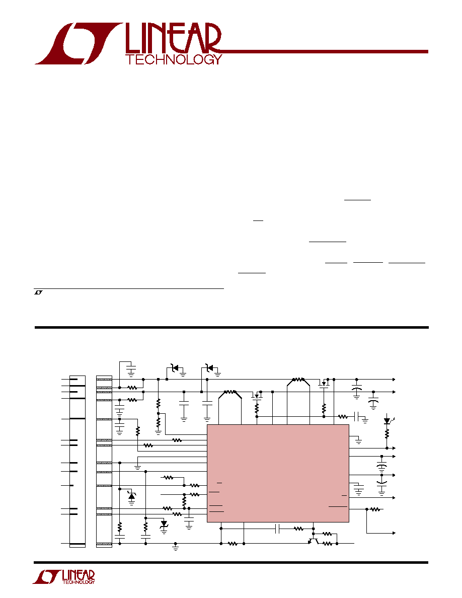
The LTC
Æ
4240 is a Hot Swap
TM
controller that allows a board
to be safely inserted and removed from a live CompactPCI
bus slot. The LTC4240 has a built-in 2-wire I
2
C compatible
interface to allow software control and monitoring of
device function and power supply status. Two external
N-channel transistors control the 3.3V and 5V supplies,
while two internal switches control the ≠12V and 12V
supplies. Electronic circuit breakers protect all four supplies
against overcurrent faults. The PWRGD output indicates
when all of the supply voltages are within tolerance. The
OFF/ON pin is used to cycle the board power or reset the
circuit breaker. The I
2
C interface allows the user to turn the
device off or on, set RESETOUT, turn on the status LED
driver and ignore 12V, ≠12V faults. It also allows the user
to read the status of the FAULT, RESETIN, RESETOUT,
PWRGD, PRSNT1# and PRSNT2# pins. Under a fault
condition, the I
2
C interface can also be used to determine
which of the four supplies generated the fault. The LTC4240
is available in a 28-pin narrow SSOP package.
s
Hot Board Insertion into CompactPCI Bus
s
Electronic Circuit Breaker
s
Allows Safe Board Insertion and Removal from a
Live CompactPCI
TM
Bus
s
I
2
C
TM
Compatible 2-Wire Interface
s
PRECHARGE Output Biases I/O Pins During Card
Insertion and Extraction
s
Controls 3.3V, 5V, 12V and ≠12V Supplies
s
Foldback Current Limit with Circuit Breaker
s
LOCAL_PCI_RST# Logic On-Board
s
QuickSwitch
Æ
Enable Output
s
Status LED Driver
s
User Programmable Supply Voltage Power-Up Rate
s
Registers Individual Supply Faults
s
Available in a 28-Pin Narrow SSOP Package
CompactPCI Hot Swap
Controller with I
2
C Compatible Interface
, LTC and LT are registered trademarks of Linear Technology Corporation.
Hot Swap is a trademark of Linear Technology Corporation.
QuickSwitch is a registered trademark of Quality Semiconductor Corp.
CompactPCI is a trademark of the PCI Industrial Computer Manufacturers Group.
I
2
C is a trademark of Philips Electronics N.V.
C5
0.01
µ
F
C1
0.047
µ
F
C4
0.01
µ
F
GND
12V
IN
V
EEIN
OFF/ON
FAULT
PWRGD
RESETIN
3V
IN
3V
IN
5V
IN
3V
SENSE
3V
OUT
5V
IN
LTC4240
PRECHARGE
DRIVE
5V
OUT
5V
SENSE
GATE
12V
OUT
V
EEOUT
TIMER
RESETOUT
EARLY
V(I/O)
R16
10k
R18
1k
R17, 1.2k
R3
10
5V
IN
R4
10
R15
2k
R30
1k
R29
10
5V
OUT
5V AT 5A
3V
OUT
3.3V AT 7.6A
12V
OUT
12V AT 500mA
V
EEOUT
≠12V AT 100mA
4240 TA01
R11
18
3V
IN
3V
OUT
R6
10k
R5
1k
R8, 1k
R7, 12
C3, 4.7nF
R9
24
R1
0.005
Q1
Si7880DP
Q2
Si7880DP
R2
0.007
C2
0.1
µ
F
R13
10
R14
10
MEDIUM 5V
LONG 5V
MEDIUM 3.3V
LONG 3.3V
LONG V(I/O)
12V
≠12V
BD_SEL#
HEALTHY#
PCI_RST#
GROUND
TO PCI BRIDGE
DEVICE OR
EQUIVALENT
BE
DGND
LED
SCL
SDA
R19
2.55k
1%
R20
1.91k
1%
PRSNT2#
PRSNT1#
ADDRIN
SCL
SDA
C8
0.01
µ
F
PER
PIN
C
LOAD
(5V
OUT
)
C
LOAD
(3V
OUT
)
C
LOAD
(12V
OUT
)
C
LOAD
(V
EEOUT
)
C7
0.01
µ
F
PER
PIN
C6
0.01
µ
F
5V
IN
Z4
Z1
Z2
Z1, Z2: SMAJ12CA
Z3, Z4: IPMT5.0AT3
Z3
CompactPCI
BACKPLANE
CONNECTOR
(FEMALE)
CompactPCI
BACKPLANE
CONNECTOR
(MALE)
LOCAL_PCI_RST#
R10
100
TO
QUICKSWITCH
Æ
ENABLE
Q3
MMBT2222A
R12
10k
R22, 2.74
R21, 1.74
R25, 1.2k
R28, 200
+
+
+
+
C9
10nF
C10
10nF
C11
10nF
LTC4240
2
4240f
Supply Voltages
5V
IN ....................................................................
≠0.3V to 12V
12V
IN .................................................................
≠0.3V to 14V
V
EEIN ...................................................................
0.3V to ≠14V
Input Voltages
PRSNT1#, PRSNT2#, SCL, RESETIN,
OFF/ON .................................................. ≠0.3V to 12V
5V
OUT
, 5V
SENSE
, 3V
IN
,
3V
SENSE
, 3V
OUT ............................
≠0.3V to (5V
IN
+ 0.3V)
ADDRIN, PRECHARGE ......................... ≠0.3V to 5V
IN
Output Voltages
TIMER, FAULT, PWRGD, SDA, RESETOUT,
LED, DRIVE, GATE, 12V
OUT .......................
≠0.3V to 14V
V
EEOUT ................................................................
≠14V to 0.3V
BE ............................................. 0.3V to (5V
IN
+ 0.3V)
Operating Temperature Range
LTC4240C ............................................... 0
∞
C to 70
∞
C
LTC4240I .............................................≠40
∞
C to 85
∞
C
Storage Temperature Range .................... 65
∞
C to 150
∞
C
Lead Temperature (Soldering, 10 sec).................. 300
∞
C
ORDER PART
NUMBER
T
JMAX
= 140
∞
C,
JA
= 135
∞
C/W
LTC4240CGN
LTC4240IGN
ABSOLUTE AXI U
RATI GS
W
W
W
U
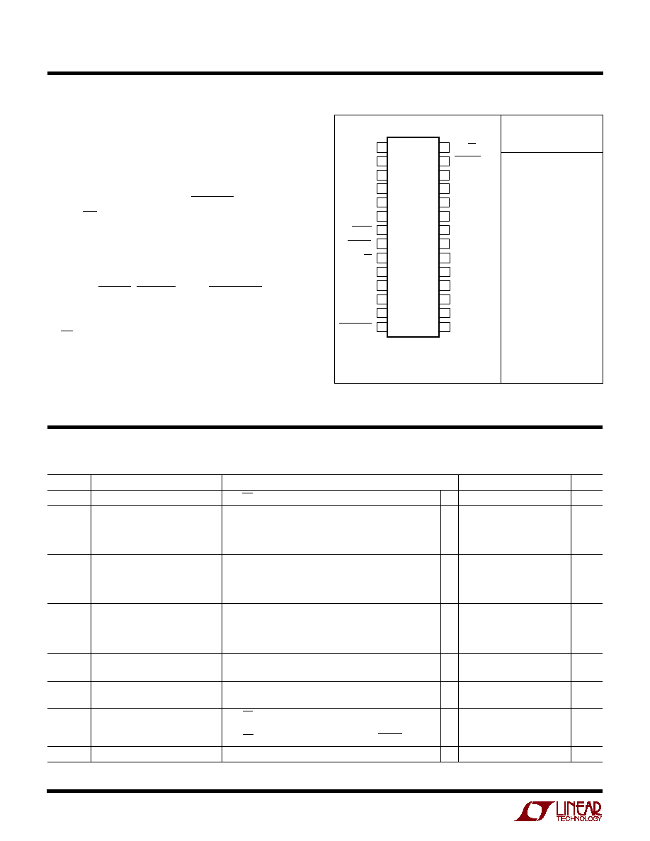
PACKAGE/ORDER I FOR ATIO
U
U
W
(Notes 1, 2)
ELECTRICAL CHARACTERISTICS
Consult LTC Marketing for parts specified with wider operating temperature ranges.
1
2
3
4
5
6
7
8
9
10
11
12
13
14
TOP VIEW
GN PACKAGE
28-LEAD PLASTIC SSOP
28
27
26
25
24
23
22
21
20
19
18
17
16
15
PRSNT1#
PRSNT2#
12V
IN
V
EEIN
TIMER
5V
OUT
FAULT
PWRGD
BE
GND
ADDRIN
SDA
SCL
RESETOUT
OFF/ON
RESETIN
12V
OUT
V
EEOUT
3V
OUT
3V
SENSE
3V
IN
5V
IN
5V
SENSE
GATE
PRECHARGE
DRIVE
DGND
LED
SYMBOL
PARAMETER
CONDITIONS
MIN
TYP
MAX
UNITS
I
DD
V
12VIN
Supply Current
OFF/ON = 0V
q
3
8
mA
V
LKO
Undervoltage Lockout
12V
IN
q
7.00
8.00
10.80
V
5V
IN
q
4.10
4.3
4.45
V
3V
IN
q
2.35
2.45
2.55
V
V
EEIN
q
≠9
≠10.5
V
V
FB
Foldback Current Limit Voltage
V
FB
= (V
5VIN
≠ V
5VSENSE
), V
5VOUT
= 0V, TIMER = 0V
q
15
25
35
mV
V
FB
= (V
5VIN
≠ V
5VSENSE
), V
5VOUT
= 3V, TIMER = 0V
q
55
70
85
mV
V
FB
= (V
3VIN
≠ V
3VSENSE
), V
3VOUT
= 0V, TIMER = 0V
q
15
25
35
mV
V
FB
= (V
3VIN
≠ V
3VSENSE
), V
3VOUT
= 2V, TIMER = 0V
q
55
65
80
mV
V
CB
Circuit Breaker Trip Voltage
V
TV
= (V
5VIN
≠ V
5VSENSE
), V
5VOUT
= 5V, TIMER = Open
q
50
55
60
mV
V
TV
= (V
5VIN
≠ V
5VSENSE
), V
5VOUT
= 0V, TIMER = Open
q
6
11
16
mV
V
TV
= (V
3VIN
≠ V
3VSENSE
), V
3VOUT
= 3.3V, TIMER = Open
q
50
55
60
mV
V
TV
= (V
3VIN
≠ V
3VSENSE
), V
3VOUT
= 0V, TIMER = Open
q
6
11
16
mV
t
OC
Overcurrent Fault Response Time
(V
5VIN
≠ V
5VSENSE
) = 100mV, TIMER = Open
q
25
35
55
µ
s
Overcurrent Fault Response Time
(V
3VIN
≠ V
3VSENSE
) = 100mV, TIMER = Open
q
25
35
55
µ
s
t
SC
Short-Circuit Response Time
(V
5VIN
≠ V
5VSENSE
) = 200mV, TIMER = Open
q
25
35
55
µ
s
(V
3VIN
≠ V
3VSENSE
) = 200mV, TIMER = Open
q
25
35
55
µ
s
I
GATE(UP)
GATE Pin Turn-On Current
OFF/ON = 0V, V
GATE
= 0V, TIMER = 0V
q
≠ 20
≠ 65
≠100
µ
A
I
GATE(DN)
GATE Pin Turn-Off Current
V
GATE
= 5V, (Note 3)
q
100
200
300
µ
A
I
GATE(FAULT)
GATE Pin Fault-Off Current
OFF/ON = 0V, V
GATE
= 2V, TIMER = Open, FAULT = 0V
q
2.5
6
8.5
mA
V
GATE
External Gate Voltage
V
GATE
= (V
12VIN
≠ V
GATE
), I
GATE
= 1
µ
A
q
600
1000
mV
The
q
denotes the specifications which apply over the full operating
temperature range, otherwise specifications are at T
A
= 25
∞
C. 12V
IN
= 12V, V
EEIN
= ≠12V, V
3VIN
= 3.3V, V
5VIN
= 5V unless otherwise noted.
LTC4240
3
4240f
The
q
denotes the specifications which apply over the full operating
temperature range, otherwise specifications are at T
A
= 25
∞
C. 12V
IN
= 12V, V
EEIN
= ≠12V, V
3VIN
= 3.3V, V
5VIN
= 5V unless otherwise noted.
ELECTRICAL CHARACTERISTICS
5V
IN
≠ 0.4
SYMBOL
PARAMETER
CONDITIONS
MIN
TYP
MAX
UNITS
V
12V
12V Switch Voltage Drop
V
12V
= (V
12VIN
≠ V
12VOUT
), I = 500mA
q
300
600
mV
V
VEE
V
EE
Switch Voltage Drop
V
VEE
= (V
EEOUT
≠ V
EEIN
), I = 100mA
q
125
250
mV
I
CL
Current Foldback
12V
IN
= 12V, 12V
OUT
= 0V
q
≠ 50
≠350
≠ 800
mA
V
EEIN
= ≠12V, V
EEOUT
= 0V
q
50
250
350
mA
I
TH
Current Fault Threshold
12V
IN
= 12V
q
≠550
≠ 1250 ≠ 1900
mA
V
EEIN
= ≠12V
q
225
500
800
mA
T
TS
Thermal Shutdown Temperature
Note 4
150
∞
C
V
TH
Power Good Threshold Voltage
12V
OUT
q
10.8
11.1
11.4
V
5V
OUT
q
4.50
4.65
4.75
V
3V
OUT
q
2.8
2.9
3.0
V
V
EEOUT
q
≠ 10
≠ 10.5
≠ 10.8
V
V
IL
Input Low Voltage
OFF/ON, RESETIN, SCL, SDA, PRSNT1#, PRSNT2#
q
0.8
V
V
IH
Input High Voltage
OFF/ON, RESETIN, SCL, SDA, PRSNT1#, PRSNT2#
q
2
V
I
IN
Input Current PRSNT1#, PRSNT2#,
OFF/ON = RESETIN = SDA = SCL = 0V, 5V,
q
±
0.08
±
2
µ
A
OFF/ON, RESETIN, SDA, SCL
PRSNT1#, PRSNT2# = 0V, 5V
q
±
0.08
±
2
µ
A
RESETOUT, FAULT Leakage Current
RESETOUT = FAULT = 12V, OFF/ON = 0V, RESETIN = 3.3V
q
±
0.08
±
2
µ
A
PWRGD Leakage Current
PWRGD = 12V, OFF/ON = 4V
q
±
0.08
±
2
µ
A
5V
SENSE
Input Current
5V
SENSE
= 5V, 5V
OUT
= 0V, GATE = 0V
q
55
100
µ
A
3V
SENSE
Input Current
3V
SENSE
= 3.3V, 3V
OUT
= 0V, GATE = 0V
q
55
100
µ
A
5V
IN
Input Current
5V
IN
= 5V, TIMER = 0V, OFF/ON = 0V
q
0.8
1.5
mA
3V
IN
Input Current
3V
IN
= 3.3V, TIMER = Open
q
250
600
µ
A
3V
IN
= 3.3V, TIMER = 0V
q
250
500
µ
A
5V
OUT
Input Current
5V
OUT
= 5V, OFF/ON = 0V, TIMER = 0V, GATE = 0V
q
237
400
µ
A
3V
OUT
Input Current
3V
OUT
= 3.3V, OFF/ON = 0V, TIMER = 0V, GATE = 0V
q
120
200
µ
A
V
EEIN
Input Current
TIMER = 0V, OFF/ON = 0V
q
≠950
≠1200
µ
A
Precharge Input Current
V
PRECHARGE
= 1V
q
10
µ
A
ADDRIN
ADDRIN = 0V, 5V
q
±
0.1
µ
A
I
TIMER
TIMER Pin Current
OFF/ON = 0V, TIMER = 0V
q
≠6
≠ 11.5
≠17
µ
A
TIMER = 5V, OFF/ON = 2V
q
15
28
55
mA
V
TIMER
TIMER Threshold Voltages
q
5
5.5
6.5
V
R
DIS
12V
OUT
Discharge Impedance
q
430
1000
5V
OUT
Discharge Impedance
q
50
100
3V
OUT
Discharge Impedance
q
150
300
V
EEOUT
Discharge Impedance
q
650
1000
V
OH
CMOS Output High Voltage
BE, I = ≠100
µ
A
q
V
V
OL
CMOS Output Low Voltage
BE, I = 100
µ
A
q
0.4
V
Output Low Voltage
PWRGD, RESETOUT, FAULT, SDA(I = 3mA)
q
0.4
V
Output Low Voltage
LED (I = 10mA)
q
0.8
V
V
PXG
PRECHARGE Reference Voltage
V
5VIN
= 5V
q
0.9
1
1.1
V
I
2
C Timing (Note 4)
f
SCL
SCL Clock Frequency
100
kHz
t
SUSTA
Start Condition Setup Time
4.7
µ
s
t
BUF
Bus Free Time Between Stop and Start
4.7
µ
s
t
HDSTA
Start Condition Hold Time
4
µ
s
LTC4240
4
4240f
SYMBOL
PARAMETER
CONDITIONS
MIN
TYP
MAX
UNITS
t
SUSTP
Stop Condition Setup Time
4
µ
s
t
HDDAT
Data Hold Time
300
ns
t
SUDAT
Data Setup Time
250
ns
t
LOW
Clock Low Period
4.7
µ
s
t
HIGH
Clock High Period
4.0
µ
s
t
f
Clock/Data Fall Time
300
ns
t
r
Clock/Data Rise Time
1000
ns
The
q
denotes the specifications which apply over the full operating
temperature range, otherwise specifications are at T
A
= 25
∞
C. 12V
IN
= 12V, V
EEIN
= ≠12V, V
3VIN
= 3.3V, V
5VIN
= 5V unless otherwise noted.
Note 3: OFF/ON pin pulled up to 5V by 1.2k resistor.
Note 4: Parameters guaranteed by design and not tested.
ELECTRICAL CHARACTERISTICS
Note 1: Absolute Maximum Ratings are those values beyond which the life
of a device may be impaired.
Note 2: All currents into device pins are positive; all currents out of
device pins are negative. All voltages are referenced to ground unless
otherwise specified.
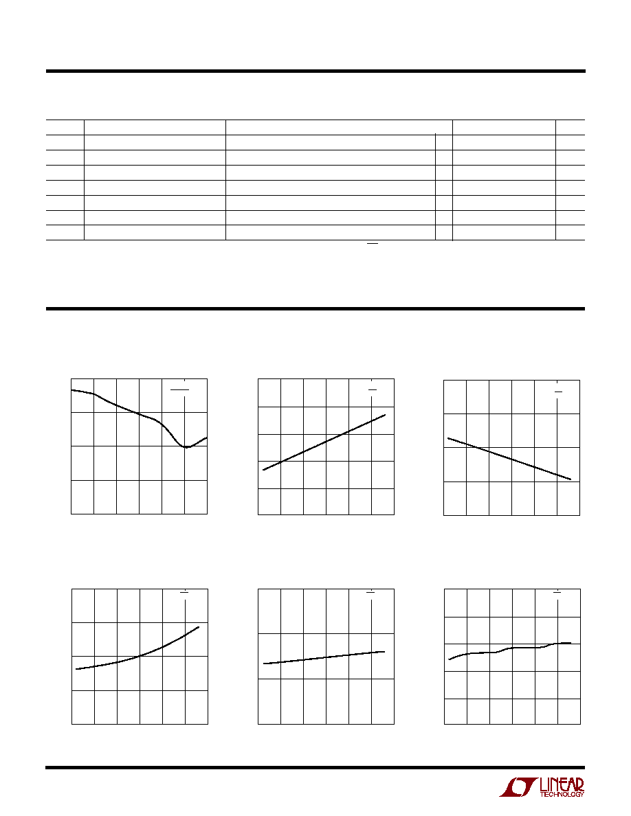
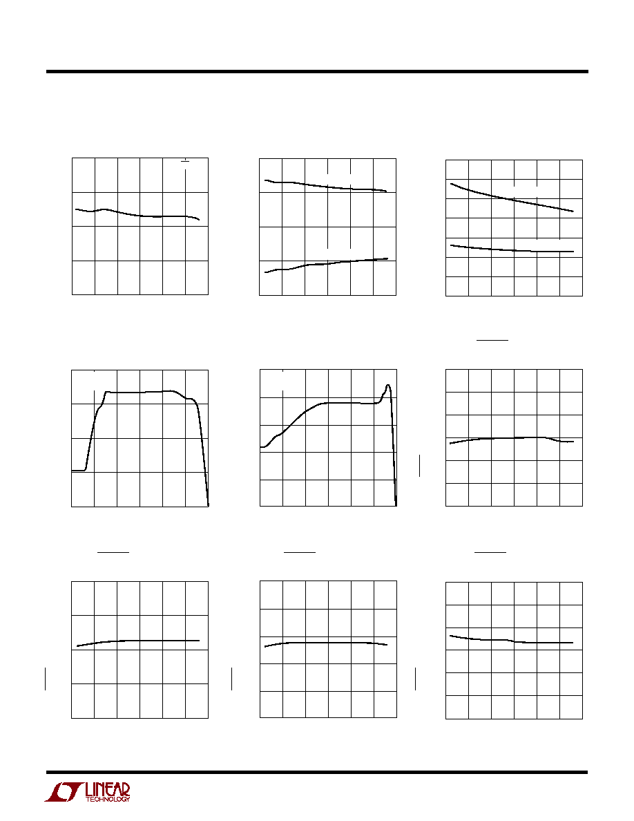
Gate Pin Fault Current
vs Temperature
Gate Pin Turn-Off Current
vs Temperature
Gate Pin Turn-On Current
vs Temperature
12V
IN
Supply Current
vs Temperature
3V
IN
Supply Current
vs Temperature
5V
IN
Supply Current
vs Temperature
TYPICAL PERFOR A CE CHARACTERISTICS
U
W
TEMPERATURE (
∞
C)
≠50
GATE PIN FAULT CURRENT (mA)
8
6
4
2
0
4.0
3.6
3.2
2.8
2.4
≠25
0
25
50
4240 G01
75
100
TEMPERATURE (
∞
C)
≠50
≠25
0
25
50
75
100
TEMPERATURE (
∞
C)
≠50
≠25
0
25
50
75
100
TEMPERATURE (
∞
C)
≠50
≠25
0
25
50
75
100
TEMPERATURE (
∞
C)
≠50
≠25
0
25
50
75
100
TEMPERATURE (
∞
C)
≠50
≠25
0
25
50
75
100
12V
IN
SUPPLY CURRENT (mA)
3V
IN
SUPPLY CURRENT (
µ
A)
5V
IN
SUPPLY CURRENT (mA)
4240 G04
GATE PIN CURRENT (
µ
A)
≠20
≠40
≠60
≠80
≠100
4240 G03
GATE PIN CURRENT (
µ
A)
350
300
250
200
150
100
280
260
240
220
1.0
0.9
0.8
0.7
0.6
0.5
4240 G02
4240 G06
4240 G05
V
GATE
= 2V
FAULT = 0V
V
GATE
= 5V
OFF/ON = 2V
V
GATE
= 0V
OFF/ON = 0V
OFF/ON = 0V
OFF/ON = 0V
OFF/ON = 0V
LTC4240
5
4240f
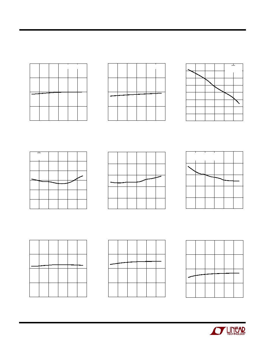
TYPICAL PERFOR A CE CHARACTERISTICS
U
W
V
EEIN
Supply Current
vs Temperature
12V
IN
Foldback Current Limit
vs Temperature
V
EEIN
Foldback Current Limit
vs Temperature
12V Output Current
≠12V Output Current
12V
OUT
PWRGD Threshold
Voltage vs Temperature
3V
OUT
PWRGD Threshold Voltage
vs Temperature
5V
OUT
PWRGD Threshold Voltage
vs Temperature
V
EEOUT
PWRGD Threshold
Voltage vs Temperature
≠0.8
≠0.9
≠1.0
≠1.1
≠1.2
TEMPERATURE (
∞
C)
≠50
≠25
0
25
50
75
100
V
EEIN
SUPPLY CURRENT (mA)
4240 G07
OFF/ON = 0V
1.6
1.2
0.8
0.4
0
OUTPUT VOLTAGE (V)
0
2
4
6
8
10
12
OUTPUT CURRENT (A)
4240 G10
12V
IN
= 12V
T
A
= 25
∞
C
3.00
2.95
2.90
2.85
2.80
TEMPERATURE (
∞
C)
≠50
≠25
0
25
50
75
100
3V
OUT
PWRGD THRESHOLD VOLTAGE (V)
4240 G13
1.6
1.2
0.8
0.4
0
TEMPERATURE (
∞
C)
≠50
≠25
0
25
50
75
100
12V
IN
FOLDBACK CURRENT LIMIT (A)
4240 G08
12V
OUT
= 10V
12V
OUT
= 0V
TEMPERATURE (
∞
C)
0.7
0.6
0.5
0.4
0.3
0.2
0.1
0
4240 G09
≠50
≠25
0
25
50
75
100
TEMPERATURE (
∞
C)
≠50
≠25
0
25
50
75
100
OUTPUT VOLTAGE (V)
0
≠2
≠4
≠6
≠8
≠10
≠12
OUTPUT CURRENT (A)
0.5
0.4
0.3
0.2
0.1
0
4240 G11
TEMPERATURE (
∞
C)
≠50
≠25
0
25
50
75
100
TEMPERATURE (
∞
C)
≠50
≠25
0
25
50
75
100
4.75
4.70
4.65
4.60
4.55
4.50
4240 G14
12V
OUT
PWRGD THRESHOLD VOLTAGE (V)
11.4
11.3
11.2
11.1
11.0
10.9
10.8
4240 G12
≠10.2
≠10.3
≠10.4
≠10.5
≠10.6
≠10.7
≠10.8
4240 G15
V
EEOUT
= ≠10V
V
EEOUT
= 0V
V
EE
FOLDBACK CURRENT LIMIT (A)
V
EEIN
= ≠12V
T
A
= 25
∞
C
5V
OUT
PWRGD THRESHOLD VOLTAGE (V)
V
EEOUT
PWRGD THRESHOLD VOLTAGE (V)
LTC4240
6
4240f
65
60
55
50
45
TEMPERATURE (
∞
C)
≠50
≠25
0
25
50
75
100
3V
SENSE
INPUT CURRENT (
µ
A)
4240 G16
3V
SENSE
= 3.3V
TEMPERATURE (
∞
C)
≠50
≠25
0
25
50
75
100
TEMPERATURE (
∞
C)
≠50
≠25
0
25
50
75
100
4240 G17
9.0
8.5
8.0
7.5
7.0
TEMPERATURE (
∞
C)
≠50
≠25
0
25
50
75
100
12V
IN
UVLO THRESHOLD VOLTAGE (V)
4240 G22
2.55
2.50
2.45
2.40
2.35
TEMPERATURE (
∞
C)
≠50
≠25
0
25
50
75
100
3V
IN
UVLO THRESHOLD VOLTAGE (V)
4240 G23
4.45
4.40
4.35
4.30
4.25
TEMPERATURE (
∞
C)
≠50
≠25
0
25
50
75
100
5V
IN
UVLO THRESHOLD VOLTAGE (V)
4240 G24
TEMPERATURE (
∞
C)
≠50
≠25
0
25
50
75
100
TEMPERATURE (
∞
C)
≠50
≠25
0
25
50
75
100
TEMPERATURE (
∞
C)
≠50
≠25
0
25
50
75
100
TIMER PIN CURRENT (
µ
A)
≠10.0
≠10.5
≠11.0
≠11.5
≠12.0
≠12.5
≠13.0
4240 G19
TIMER THRESHOLD VOLTAGE (V)
6.0
5.8
5.6
5.4
5.2
5.0
4240 G20
CIRCUIT BREAKER RESPONSE TIME (
µ
s)
40
38
36
34
32
30
4240 G21
TIMER PIN CURRENT (mA)
4240 G18
34
32
30
28
26
24
22
20
18
5V
SENSE
= 5V
OFF/ON = 0V
V
TIMER
= 0V
OFF/ON = 2V
V
TIMER
= 5V
65
60
55
50
45
5V
SENSE
INPUT CURRENT (
µ
A)
TIMER PIN FLOATING
V
IN
≠
V
SENSE
= 0.1V
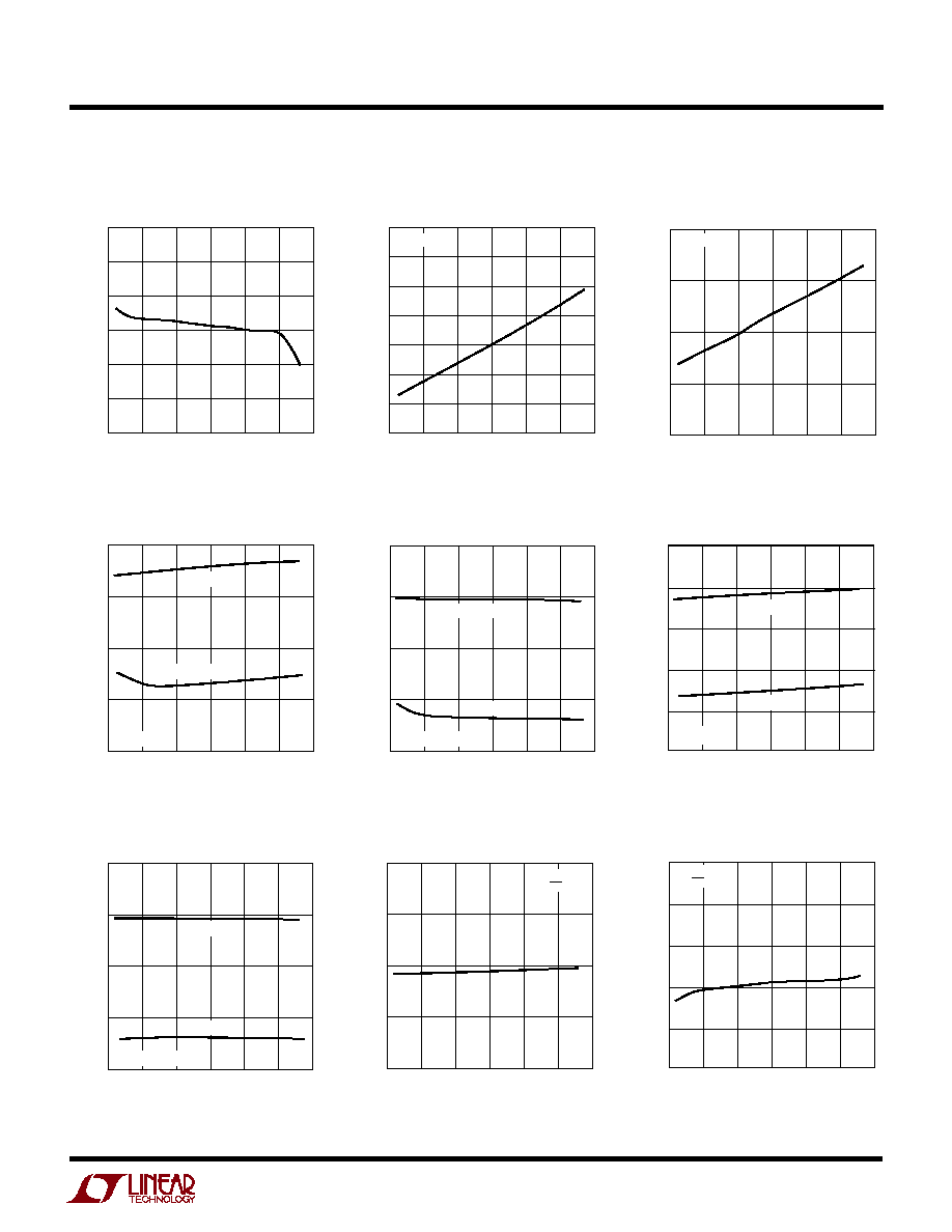
3V
SENSE
Input Current
vs Temperature
Timer Pin Turn-Off Current
vs Temperature
Timer Pin Turn-On Current vs
Temperature
Timer Threshold Voltage
vs Temperature
5V/3.3V Circuit Breaker
Overcurrent Fault Response Time
vs Temperature
3V
IN
UVLO Threshold Voltage
vs Temperature
5V
IN
UVLO Threshold Voltage
vs Temperature
12V
IN
UVLO Threshold Voltage
vs Temperature
TYPICAL PERFOR A CE CHARACTERISTICS
U
W
5V
SENSE
Input Current
vs Temperature
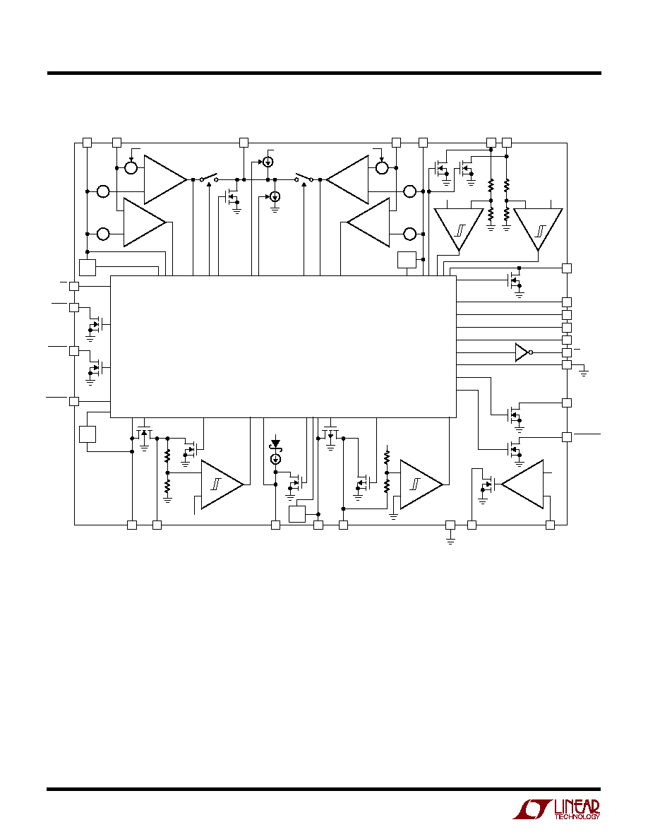
LTC4240
7
4240f
TEMPERATURE (
∞
C)
≠50
≠25
0
25
50
75
100
V
EEIN
UVLO THRESHOLD VOLTAGE (V)
≠7.6
≠8.0
≠8.4
≠8.8
≠9.2
≠9.6
≠10.0
4240 G25
160
140
120
100
80
TEMPERATURE (
∞
C)
≠50
≠25
0
25
50
75
100
3V
OUT
INPUT CURRENT (
µ
A)
4240 G33
80
60
40
20
0
TEMPERATURE (
∞
C)
≠50
≠25
0
25
50
75
100
4240 G32
80
60
40
20
0
TEMPERATURE (
∞
C)
≠50
≠25
0
25
50
75
100
3V CIRCUIT BREAKER TRIP VOLTAGE (mV)
5V CIRCUIT BREAKER TRIP VOLTAGE (mV)
5V FOLDBACK CURRENT LIMIT VOLTAGE (mV)
4240 G29
200
160
120
80
40
TEMPERATURE (
∞
C)
≠50
≠25
0
25
50
75
100
V
EE
INTERNAL SWITCH VOLTAGE DROP (mV)
4240 G27
80
60
40
20
0
TEMPERATURE (
∞
C)
≠50
≠25
0
25
50
75
100
3V FOLDBACK CURRENT LIMIT VOLTAGE (mV)
4240 G28
TEMPERATURE (
∞
C)
≠50
≠25
0
25
50
75
100
4240 G31
TEMPERATURE (
∞
C)
12V INTERNAL SWITCH VOLTAGE DROP (mV)
500
450
400
350
300
250
200
150
4240 G26
≠50
≠25
0
25
50
75
100
I = 500mA
V
TIMER
= 0V
V
TIMER
= OPEN
V
TIMER
= OPEN
I = 100mA
3V
OUT
= 0V
3V
OUT
= 2V
3V
OUT
= 3.3V
3V
OUT
= 0V
V
TIMER
= 0V
5V
OUT
= 3V
5V
OUT
= 0V
5V
OUT
= 5V
5V
OUT
= 0V
3V
OUT
= 3.3V
OFF/ON = 0V
5V
OUT
INPUT CURRENT (
µ
A)
300
280
260
240
220
200
4240 G34
5V
OUT
= 5V
OFF/ON = 0V
TEMPERATURE (
∞
C)
≠50
≠25
0
25
50
75
100
100
80
60
40
20
0
3V Foldback Current Limit Voltage
vs Temperature
3V Circuit Breaker Trip Voltage
vs Temperature
5V Foldback Current Limit Voltage
vs Temperature
5V Circuit Breaker Trip Voltage
vs Temperature
3V
OUT
Input Current
vs Temperature
V
EEIN
UVLO Threshold Voltage
vs Temperature
12V
IN
Internal Switch Voltage
Drop vs Temperature
V
EEIN
Internal Switch Voltage Drop
vs Temperature
TYPICAL PERFOR A CE CHARACTERISTICS
U
W
5V
OUT
Input Current
vs Temperature

LTC4240
8
4240f
PWRGD (Pin 8): Open-Drain Power Good Output. Con-
nect the CPCI HEALTHY# signal to the PWRGD pin.
PWRGD remains low while V
12VOUT
11.1V, V
3VOUT
2.9V, V
5VOUT
4.65V and V
EEOUT
≠10.5V. When any of
the supplies drops below its power good threshold volt-
age, PWRGD will go high after a 10
µ
s deglitching time. The
switches will not be turned off when PWRGD goes high,
unless a fault has occurred. The CPCI specification calls
for a 0.01
µ
F bypass capacitor on the backplane for
HEALTHY#.
BE (Pin 9): QuickSwitch Bus Enable Output. The BE output
remains high until power is good on all supplies. This
serves to isolate the I/O data lines during live
insertion. This is a CMOS output powered by 5V
IN
.
GND (Pin 10): Analog Ground. Connect to analog ground
plane.
ADDRIN (Pin 11): I
2
C Address Programming Input. The
I
2
C address is programmed by connecting the ADDRIN
pin to a resistor divider between the 5V
IN
pin and GND. See
Table 1 for 1% resistor values and corresponding ad-
dresses. Resistors must be placed close to the ADDRIN
pin to minimize errors due to stray capacitance and
resistance on the board trace. Connect this pin to ground
if I
2
C is not used.
SDA (Pin 12): I
2
C Data Input and Output. Note that TTL
levels are used. Connect this pin to ground if I
2
C is not
used.
SCL (Pin 13): I
2
C Clock Input, 100kHz Maximum. Note
that TTL levels are used. Do not float. Connect this pin to
ground if I
2
C is not used.
RESETOUT (Pin 14): Open-Drain Reset Output. Connect
the CPCI LOCAL_PCI_RST# signal to the RESETOUT pin.
RESETOUT is the logical combination of RESETIN, PWRGD,
and I
2
C RESETOUT latch output.
LED (Pin 15): CPCI Status LED. Pulls low to light LED
when RESETOUT is low or when the I
2
C LED latch is set.
DGND (Pin 16): Digital Ground. Connect to ground plane.
DRIVE (Pin 17): External transistor's base drive output for
bus precharge. Connects to the base of an external NPN
emitter-follower which in turn biases the PRECHARGE
PRSNT1# (Pin 1): PCI Present Detect Input 1. PRSNT1#
and PRSNT2# are readable over the I
2
C Bus. PRSNT1#
and PRSNT2# indicate the maximum power used by the
card. Do not float.
PRSNT2# (Pin 2): PCI Present Detect Input 2. Do not float.
12V
IN
(Pin 3): 12V Supply Input. A 0.5
switch is inter-
nally connected between 12V
IN
and 12V
OUT
with foldback
current limit. An undervoltage lockout circuit prevents the
switches from turning on while the 12V
IN
pin is below 8V.
12V
IN
provides power to some of the LTC4240's internal
circuitry. See Input Transient Protection section on how to
protect 12V
IN
from large voltage transients.
V
EEIN
(Pin 4): ≠12V Supply Input. A 1
internal switch is
connected between V
EEIN
and V
EEOUT
with foldback cur-
rent limit. An undervoltage lockout circuit prevents the
switches from turning on while V
EEIN
is above ≠ 9V. See
Connecting V
EEIN
section for more notes on V
EEIN
and
V
EEOUT
. Also refer to Input Transient Protection section.
TIMER/AUX 12V
IN
(Pin 5): Current Fault Inhibit Timing
Input. Connect a capacitor from TIMER to GND. With the
LTC4240 turned off (OFF/ON = HIGH), the TIMER pin is
internally held at GND. When the device is turned on, an
11.5
µ
A pull-up current source is connected to TIMER.
Current limit faults will be ignored until the voltage at the
TIMER pin rises above 5.5V. The Timer capacitor also
serves as an auxiliary charge reservoir for internal V
CC
in
the event the 12V
IN
pin voltage glitches below the LTC4240
UVL threshold voltage.
5V
OUT
(Pin 6): 5V Output Sense. The PWRGD pin will not
pull low until the 5V
OUT
pin voltage exceeds 4.65V. When
the power switches are turned off, a 50
resistor pulls
5V
OUT
to ground.
FAULT (Pin 7): Open-Drain Fault Output . FAULT is pulled
low when a current limit fault is detected. Current limit
faults are ignored until the voltage at the TIMER pin is
above 5.5V. Once the TIMER cycle is complete, FAULT
pulls low and the LTC4240 turns off (in the event of an
overcurrent fault lasting longer than 35
µ
s). The LTC4240
will remain in the off state until the OFF/ON pin is cycled
high then low or power is cycled. Note that the OFF/ON
cycling can also be performed using I
2
C bus.
U
U
U
PI FU CTIO S

LTC4240
9
4240f
long pin must be connected to 3V
IN
to ensure precharge
output. See Input Transient Protection section.
3V
SENSE
(Pin 23): 3.3V Current Limit Sense. A sense
resistor placed between 3V
IN
and 3V
SENSE
determines the
current limit for this supply. A foldback feature makes the
current limit decrease as the voltage at the 3V
OUT
pin
approaches 0V. To disable current limit, 3V
SENSE
and 3V
IN
must be tied together.
3V
OUT
(Pin 24): 3.3V Output Sense. The PWRGD pin
cannot pull low until the 3V
OUT
pin voltage exceeds 2.9V.
If no 3.3V input supply is available, tie the 3V
OUT
pin to the
5V
OUT
pin. When the power switches are turned off, a
150
resistor pulls 3V
OUT
to ground.
V
EEOUT
(Pin 25): ≠12V Supply Output. An internal 1
switch is connected between V
EEIN
and V
EEOUT
. V
EEOUT
must exceed ≠10.5V before the PWRGD pin pulls low.
When the power switches are turned off, a 650
resistor
pulls V
EEOUT
to ground.
12V
OUT
(Pin 26): 12V Supply Output. A 0.5
switch is
connected between 12V
IN
and 12V
OUT
. 12V
OUT
must
exceed 11.1V before the PWRGD pin can pull low. When
the power switches are turned off, a 430
resistor pulls
12V
OUT
to ground.
RESETIN (Pin 27): PCI Reset Input. Connect the CPCI
PCI_RST# signal to the RESETIN pin. Pulling RESETIN low
will cause RESETOUT to pull low. Note that the I
2
C
RESETIN latch output can also set RESETOUT. Do not
float.
OFF/ON (Pin 28): OFF/ON Input. Connect the CPCI
BD_SEL# signal to the OFF/ON pin. When the OFF/ON pin
is pulled low, the GATE pin is pulled high by a 65
µ
A current
source and the internal 12V and ≠12V switches are turned
on. When the OFF/ON pin is pulled high, the GATE pin will
be pulled to ground by a 200
µ
A current source and the 12V
and ≠12V switches turn off.
Cycling the OFF/ON pin high and low will reset a tripped
circuit breaker and start a new power-up sequence. The
I
2
C OFF/ON latch output can also be used to reset the
electronic circuit breaker. Do not float.
node. An external 1k resistor between the transistor's base
and 3V
IN
is needed.
PRECHARGE (Pin 18): Precharge Monitor Input. An inter-
nal error amplifier servos the DRIVE pin voltage to keep the
precharge node at 1V. Becomes valid when long 5V and
3.3V power pins make contact .Tie pins 17 and 18 together
if precharge function is unused.
GATE (Pin 19): High Side Gate Drive for the External 3.3V
and 5V N-Channel Power Transistors. An external series
RC network is required for the current limit loop compen-
sation and to set the maximum ramp-up rate. During
power-up, the slope of the voltage rise at the GATE pin is
set by the 65
µ
A current source charging the external GATE
capacitor or by the 3.3V or 5V current limit and the
associated output capacitor. During power-down, a 200
µ
A
current source pulls the GATE pin to GND.
The voltage at the GATE pin will be modulated to maintain
a constant current when either the 3.3V or 5V supply goes
into current limit and the TIMER pin is less than 5.5V. Once
the TIMER pin is above 5.5V, and in the event of a current
fault condition lasting for longer than 35
µ
s, the GATE pin
is immediately pulled to GND.
5V
SENSE
(Pin 20): 5V Current Limit Sense. A sense resistor
placed between 5V
IN
and 5V
SENSE
determines the current
limit for this supply. A foldback current feature makes the
current limit decrease as the voltage at the 5V
OUT
pin
approaches 0V. To disable the current limit, 5V
SENSE
and
5V
IN
must be tied together.
5V
IN
(Pin 21): 5V Supply Sense Input. An undervoltage
lockout circuit prevents the switches from turning on
when the voltage at the 5V
IN
pin is less than 4.3V. At least
one long pin must be connected to 5V
IN
to ensure precharge
output. See Input Transient Protection section.
3V
IN
(Pin 22): 3.3V Supply Sense Input. An undervoltage
lockout circuit prevents the switches from turning on
when the voltage at the 3V
IN
pin is less than 2.45V. If no
3.3V input supply is available, connect two series diodes
between 5V
IN
and 3V
IN
(tie anode of first diode to 5V
IN
and
cathode of second diode to 3V
IN
, Figure 15). At least one
U
U
U
PI FU CTIO S
LTC4240
10
4240f
65mV,
TIMER LO
165mV,
TIMER HI
Q8
Q14
V
EEIN
4
TIMER
5
V
EEOUT
25
3V
OUT
24
5V
OUT
6
≠
+
+≠
Q11
Q10
200
µ
A
65
µ
A
GATE
5V
OUT
55mV
12V
in
19
5V
SENSE
20
12V
IN
3
12V
OUT
26
5V
IN
21
≠
+
+≠
+≠
4.3V
UVL
≠9V
UVL
8V
UVL
≠
+
+≠
3V
OUT
55mV
3V
SENSE
23
3V
IN
22
RESETOUT
14
1
9
11
13
2
≠
+
≠
+
≠
+
+≠
+≠
2.45V
UVL
Q6
1V
1.2V
1.2V
≠
+
1.2V
≠
+
1.2V
≠
+
LED
15
Q5
DGND
16
Q3
Q2
SDA
SCL
ADDRIN
PRSNT2#
PRSNT1#
BE
12
Q4
RESETIN 27
PWRGD 8
Q12
FAULT 7
Q13
OFF/ON 28
Q7
Q9
11.5
µ
A
12V
IN
GND
10
DRIVE
17
PRECHARGE
4240 BD
18
LOGIC
Q1
CP3
CP2
CP4
A2
A1
CP1
CP6
CP5
A3
V
CB
V
CB
70mV,
TIMER LO
165mV,
TIMER HI
BLOCK DIAGRA
W

LTC4240
11
4240f
The LTC4240 is a Hot Swap controller that allows a board
to be safely inserted and removed from a CompactPCI bus
slot. The LTC4240 has built-in 2-wire I
2
C compatible
interface hardware to allow software control and monitor-
ing of device function and power supply status.
Hot Circuit Insertion
When a circuit board is inserted into a live CompactPCI
(CPCI) backplane slot, supply bypass capacitors on the
board can draw huge supply transient currents from the
CPCI backplane power bus. The transient currents can
cause glitches on the power bus, thus causing other
boards in the system to reset.
The LTC4240 is designed to turn a board's supply voltages
on and off in a controlled manner, allowing the board to be
safely inserted or removed from a live CPCI slot without
disturbing the system power supplies. The device also
protects the supplies from shorts, precharges the bus I/O
pins during insertion and extraction and monitors the
supply voltages. The LTC4240 includes an I
2
C compatible
interface, which allows software control of device func-
tions.
The LTC4240 is specifically designed for CPCI applica-
tions where it resides on the plug-in board. For best
results, a well bypassed backplane is recommended.
LTC4240 Feature Summary
∑ Allows safe board insertion and removal from a CPCI
backplane. Status LED visually identifies when a board
is ready for removal.
∑ Controls all four CPCI supplies: ≠12V, 12V, 3.3V and
5V.
∑ Foldback current limit: An analog current limit with a
value that depends on the output voltage. If the output
is shorted to ground, the current limit drops to keep
power dissipation and supply glitches to a minimum.
∑ 12V and ≠12V circuit breakers: if either supply remains
in current limit for more than 35
µ
s, the circuit breaker
will trip, the supplies will turn off and the FAULT pin
pulls low.
∑ Adjustable 5V and 3.3V circuit breakers: if either supply
exceeds current limit for more than 35
µ
s, the circuit
breaker will trip, the supplies will be turned off and the
FAULT pin will be pulled low. In addition, an analog loop
will servo the GATE pin to limit the current to three times
circuit breaker limit during transient conditions.
∑ I
2
C interface: software control allows user to both write
to and read from the device. The user can turn the
device off and on, set the status LED, set RESETOUT
and disable faults on 12V
IN
and V
EEIN
. The user can also
read the device status: FAULT, RESETIN, RESETOUT
PWRGD, PRSNT1#, PRSNT2#, FAULTCODE0 and
FAULTCODE1. If a fault occurs, the FAULTCODE bits
identify which supply generated the fault.
∑ Current limit during power-up: the supplies are allowed
to power-up in current limit. This allows the LTC4240 to
power-up boards with widely varying capacitive loads
without tripping the circuit breaker. The maximum
allowable power-up time is programmable using an
external capacitor connected to the TIMER pin. See
TIMER section
∑ Internal 12V and ≠12V power switches.
∑ PWRGD output: indicates the voltage status of the four
supply voltages.
∑ PCI_RST# is combined with HEALTHY# and
with the I
2
C RESETIN latch output to create
LOCAL_PCI_RST# output. If HEALTHY# asserts,
LOCAL_PCI_RST# is asserted independent of the other
two inputs.
∑ Precharge output: an internal reference and amplifier
provide 1V for biasing bus I/O connector pins during
CPCI card insertion and extraction.
∑ Space saving 28-pin SSOP package.
I
2
C Interface
The LTC4240 incorporates an I
2
C compatible 2-wire (clock
and data) interface that allows the user to easily query and
control the status of the LTC4240. A single analog input
pin selects 1 of 32 allowed addresses. The I
2
C bus can be
APPLICATIO S I FOR ATIO
W
U
U
U

LTC4240
12
4240f
used to turn off/on the power switches, turn on the status
LED (alerting the user that its safe to remove the plug-in
board), and assert the LOCAL_PCI_RST# signal. The I
2
C
bus is also used to read the logic signals of several device
pins: FAULT, PWRGD, RESETIN, and RESETOUT. Addi-
tionally, when a supply generates a current fault, the I
2
C
bus can be used to determine which supply generated the
fault. See Send Byte and Receive Byte sections for a full
description of all I
2
C features.
The LTC4240 supports Send Byte and Receive Byte proto-
cols. Communication is achieved using the SCL and SDA
pins (TTL compatible input thresholds). The SCL pin is the
clock input from the I
2
C bus (host) to the LTC4240 (slave).
The maximum SCL frequency is 100kHz. SDA is the
bidirectional data transfer line between the I
2
C bus and the
LTC4240. Send Byte and Receive Byte protocols are both
comprised of 2 bytes. The first byte for both is the address
byte. All communication begins with a START command.
Programming the I
2
C Address
The voltage on the ADDRIN pin determines the I
2
C ad-
dress. The ADDRIN voltage is set externally with a resistor
divider from 5V
IN
to ground (resistor placement must be
close to the pin, do not place a bypass capacitor on
ADDRIN). This voltage is fed to a 5-bit A/D and compared
against the address byte clocked in by the I
2
C bus. The 5-
bit A/D allows 32 unique LTC4240 devices to be connected
on the same I
2
C bus. 1% resistors should be used to place
the voltage at ADDRIN approximately 0.5 LSB away from
each code transition. Table 1 shows recommended resis-
tor values for each of the address code segments. The
resistor ratio for each code segment has been optimized
for best performance over the specified temperature range.
The parallel resistance for the address setting resistors
should be kept under 10k.
APPLICATIO S I FOR ATIO
W
U
U
U
Table 1. Suggested ADDRIN 1% Resistor Values
ADDR RECOMMENDED ALLOWED ADDRIN
R
19(TOP)
R
20(BOT)
CODE ADDRIN VOLTAGE VOLTAGE RANGE
RESISTOR
RESISTOR
00
0.108125
0.080 to 0.136
8660
191
01
0.264375
0.236 to 0.293
2550
140
02
0.420625
0.393 to 0.449
2550
237
03
0.576875
0.549 to 0.605
2550
332
04
0.733125
0.705 to 0.761
2550
442
05
0.889375
0.861 to 0.918
2550
549
06
1.045625
1.018 to 1.074
3830
1020
07
1.201875
1.174 to 1.230
2550
806
08
1.358125
1.330 to 1.386
2550
953
09
1.514375
1.486 to 1.543
1150
499
10
1.670625
1.643 to 1.699
1020
511
11
1.826875
1.799 to 1.860
8660
4990
12
1.983125
1.955 to 2.021
2550
1690
13
2.139375
2.111 to 2.175
2550
1910
14
2.295625
2.268 to 2.330
1130
1130
15
2.451875
2.424 to 2.488
1370
1330
16
2.608125
2.580 to 2.644
2550
2800
17
2.764375
2.736 to 2.800
2550
3160
18
2.920625
2.888 to 2.950
2550
3570
19
3.076875
3.044 to 3.110
715
1150
20
3.233125
3.200 to 3.262
1150
2100
21
3.389375
3.356 to 3.421
1150
2430
22
3.545625
3.513 to 3.574
1150
2800
23
3.701875
3.669 to 3.731
357
1020
24
3.858125
3.825 to 3.886
2550
8660
25
4.014375
3.981 to 4.041
249
1020
26
4.170625
4.138 to 4.190
1070
5360
27
4.326875
4.294 to 4.349
178
1150
28
4.483125
4.450 to 4.499
133
1150
29
4.639375
4.606 to 4.651
102
1300
30
4.795625
4.763 to 4.805
105
2430
31
4.951875
4.919 to 4.962
100
10000

LTC4240
13
4240f
APPLICATIO S I FOR ATIO
W
U
U
U
START and STOP Commands
The START command is defined as a high to low transition
of the SDA line while the SCL line is high. It is an asynchro-
nous event issued by the host, waking up all slave devices
and alerting them that a slave address is being written onto
the bus. Only the slave device that matches the address will
communicate with the host. The STOP command is de-
fined as a low to high transition on the SDA line while SCL
is high. It is also an asynchronous event issued by the host
to signal the termination of the data transfer. Other than
START and STOP commands, the SDA line is allowed to
change states only when SCL is low.
Address Byte
Once the LTC4240 has detected a START command, it
clocks in the SDA line on the succeeding 9 SCL rising
edges. The first 7 bits clocked in contain the address of the
slave device targeted by the host. The first (MSB) address
bit must be set to low and the second bit must be set to
high. The next 5 bits are fed into a digital comparator and
compared against the output of an internal 5-bit A/D. If the
comparison is true, then there is an address match and the
LTC4240 continues to communicate with the host device.
The LTC4240 proceeds to acknowledge the address match
by pulling the SDA line low while SCL is low, just before the
9th SCL rising edge. Figures 1 and 3 show a timing
diagram of the START condition and address byte for both
the Send Byte and Receive Byte protocols. Note that the
SDA bit clocked in with the 8th SCL edge determines
whether the host is sending or receiving information to/
from the LTC4240.
Send Byte Protocol
The Send Byte protocol allows a host to write information
into the LTC4240 and command the LTC4240 to perform
certain predetermined functions. The host initiates com-
munication with a START bit followed by 7 address bits.
The address bits are followed by the R/W bit, which is low
for Send Byte. The 9th bit is asserted low by the LTC4240
to acknowledge when there has been an address match.
The only time the LTC4240 writes data onto the SDA bus
during a send byte is to acknowledge the address and
command bytes. The first 8 bits are referred to collectively
as the address byte.
The command byte follows the address byte. The
command byte contains the information sent from the
host to the LTC4240. After the LTC4240 acknowledges the
address byte, each of the next 8 SCL rising edges shifts
SDA from the host into a shift register inside the LTC4240.
The first 2 bits clocked into the shift register (2 MSBs of the
command latch) are not used by the LTC4240. Only the 6
LSBs are stored in the command latch on the falling edge
of the 8th clock during the command byte. The output of
the command latch remains fixed until the next Send Byte
command overwrites it. Note that if power is turned off
(5V
IN
< 2V), the command and data latches will be cleared.
Figure 1 shows the timing diagram of the entire send byte
protocol. Transmission ends when the host issues a STOP
command. Table 2 defines the functions of the 6 command
bits. Note that some of these functions can override, or can
be overridden by, other circuitry and pins of the LTC4240.
Figure 2 shows the relationship between bits C1 to C3 and
other LTC4240 signals.
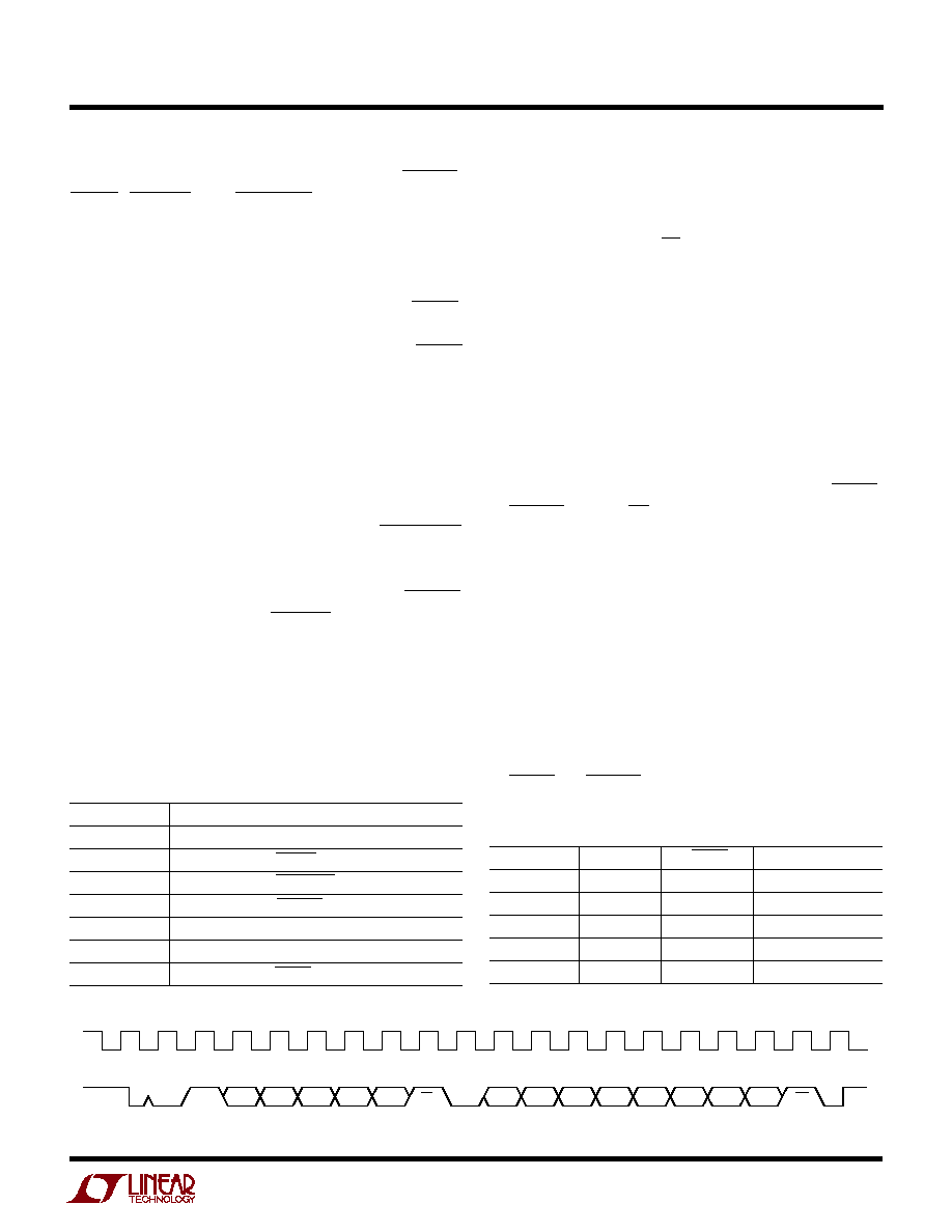
Receive Byte Protocol
The Receive Byte protocol is used by the host to read data
from the LTC4240 data latch. This protocol begins with a
START command, issued by the host, followed by 7
address bits. The address bits are followed by the R/W bit,
which is high for Receive Byte. The 9th bit is used by the
LTC4240 to acknowledge when there is an address match.
The data byte then follows the address byte. This byte
contains LTC4240 status information. After the LTC4240
acknowledges the address byte, it shifts 8 bits of data onto
the SDA line. Figure 3 shows the entire Receive Byte timing
diagram. Note that neither the host or the slave acknowl-
edges the data byte (SDA line stays high during 9th clock
edge of the data byte).
LTC4240
14
4240f
APPLICATIO S I FOR ATIO
W
U
U
U
Table 2. Command Byte Definitions
HIGH
LOW
POWER-UP STATE
C7
Don't care
Don't care
N/A
C6
Don't care
Don't care
N/A
C5
Ignore V
EEOUT
faults
Don't ignore V
EEOUT
faults
LOW
C4
Ignore 12V
OUT
faults
Don't ignore 12V
OUT
faults
LOW
C3
Sets RESETOUT
Does not set RESETOUT low
LOW
C2
Turns OFF/ON to OFF
Does not set OFF/ON
LOW
Overrides OFF/ON pin
Does not override OFF/ON pin
C1
Turns on LED open drain
Does not turn on LED open drain
LOW
C0
Don't care
Don't care
N/A
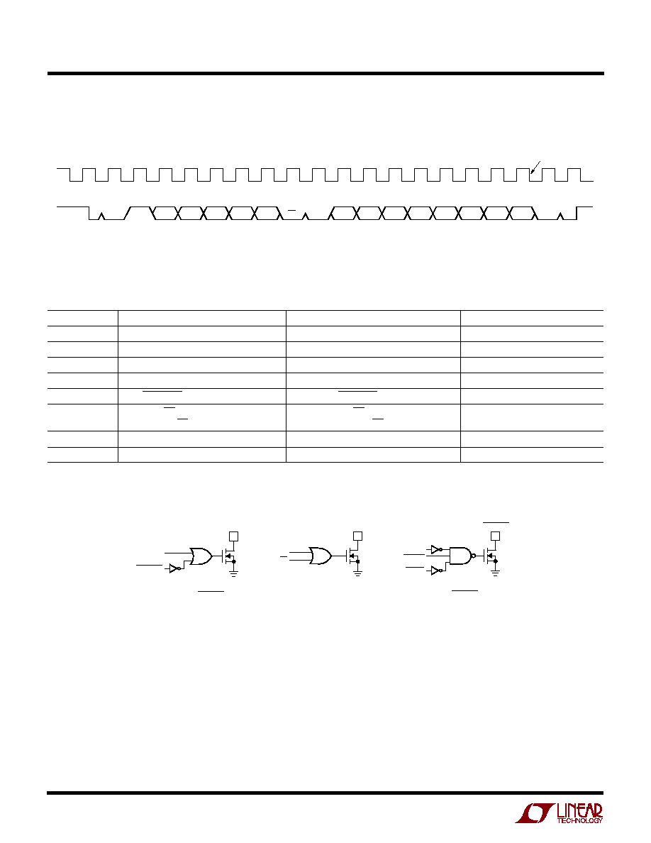
Figure 1. Send Byte Protocol
Figure 2. Send Byte Command Latch and Logic
SCL
1
2
3
4
5
6
7
8
9
1
2
3
4
5
6
7
8
9
STOP
SDA
START
ACK
ACK
R/WR=0
ADDR 4
ADDR 3
ADDR 2
ADDR 1
ADDR 0
C5
C4
C3
C2
C1
XX
0
1
XX
XX
LATCH
COMMAND BYTE
ADDRESS BYTE
COMMAND BYTE
4240 F01
4240 F02
C3 IS USED TO SET
LOCAL_PCI_RST# (RESETOUT).
C2 PULLS DOWN THE GATE OF THE
EXTERNAL N-CHANNEL SWITCHES. IT
ALSO TURNS OFF THE 12V
IN
AND V
EEIN
INTERNAL POWER SWITCHES.
C3
C2
C1
RESETIN
PWRGD
OFF/ON
GATE
RESETOUT
RESETOUT
LED
C1 TURNS ON THE EXTERNAL STATUS
LED INDEPENDENT OF RESETOUT.
LTC4240
15
4240f
Table 3 shows the definition for each data bit. PWRGD,
FAULT, RESETIN, and RESETOUT external pins can be
monitored. PRSNT1# and PRSNT2# are PCI signals that
provide information on the power requirements of the
board. Refer to PCI local bus specifications for a detailed
description. FAULTCODE1 and FAULTCODE0 are two in-
ternal binary encoded signals that, along with FAULT,
indicate which of the four supplies generated a fault. Note
that the FAULTCODE signals are valid only when FAULT
has been asserted low. See Table 4 for description.
Status LED
The main function of the LED is to alert the user when it is
permissible to physically extract the board. The LED
output of the LTC4240 is an open drain N-channel device
capable of sinking 10mA from an externally connected
LED. This LED lights up when RESETOUT
(LOCAL_PCI_RST#) is asserted. Upon application of Early
Power, the long 5V pins will power up the LTC4240 and
light up the Status LED. It will remain on until PWRGD
(HEALTHY#) is asserted and RESETIN (PCI_RST#) is de-
asserted, and the board enters normal operation. Note that
this LED can also be turned on via the I
2
C 2-wire interface.
CPCI Connection Pin Sequence
The staggered length of the CPCI male connector pins
ensures that all power supplies are physically connected
APPLICATIO S I FOR ATIO
W
U
U
U
Table 3. STATUS Byte Definitions
S7
Logic state of the PRSNT2# pin
S6
Logic state of the PRSNT1# pin
S5
Logic state of the PWRGD pin
S4
Logic state of the RESETOUT pin
S3
Logic state of the RESETIN pin
S2
FAULTCODE1 (see Table 4)
S1
FAULTCODE0 (see Table 4)
S0
Logic state of the FAULT pin
Table 4. FAULTCODE Encoding Description for Receive Byte
FAULTCODE0
FAULTCODE1
FAULT
Supply Causing Fault
LO
LO
LO
3V
IN
LO
HI
LO
5V
IN
HI
LO
LO
12V
IN
HI
HI
LO
V
EEIN
X
X
HI
None
SCL
1
2
3
4
5
6
7
8
9
1
2
3
4
5
6
7
8
9
STOP
SDA
START
ACK
ACK
R/WR=1
ADDR 4
ADDR 3
ADDR 2
ADDR 1
ADDR 0
S5
S4
S3
S2
S1
S0
0
1
S7
S6
ADDRESS BYTE
DATA BYTE
4240 F03
Figure 3. Receive Byte Protocol
to the LTC4240 before back-end power is allowed to ramp
(BD_SEL# asserted low). The long pins, which include 5V,
3.3V, V(I/O) and GND mate first. The short pins, which
includes BD_SEL# (OFF/ON), mate last. At least one long
5V power pin must be connected to the LTC4240 in order
for the PRECHARGE voltage to be available during Early
Power. The external components connected to the
precharge pin require long 3.3V.
The following is a typical hot plug sequence:
1. ESD clips make contact.
2. Long power and ground pins make contact and Early
Power is established (see Early Power section). The 1V
PRECHARGE voltage becomes valid at this stage. Power
is applied to the pull-up resistors connected to FAULT,
PWRGD and OFF/ON pins. The status LED is lit, indicat-
ing that the plug-in board is in the process of being
connected (LOCAL_PCI_RST# is asserted). All power
switches are off.
3. Medium length pins make contact. There are six 5V and
eight 3.3V medium length power pins, bringing the 5V
total to 8 pins and the 3.3V total to 10 pins. The
maximum DC current for the 3.3V and 5V supplies is
10A and 8A, respectively. The I
2
C command latch is
initialized to allow seamless CPCI Hot Swap operation.
The LTC4240 can be used as a Hot Swap controller
without ever establishing I
2
C communication. Both
FAULT and PWRGD continue to be pulled up high at this
LTC4240
16
4240f
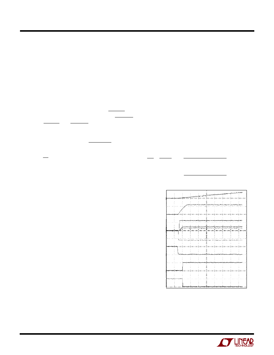
A high to low transition on BD_SEL# causes the voltages
on the TIMER, GATE, 3V
OUT
, 5V
OUT
, 12V
OUT
and V
EEOUT
pins to begin ramping (see Figure 4). The TIMER pin
capacitance is charged by an 11.5
µ
A current source while
the GATE capacitance is charged by a 65
µ
A current source.
Concurrently, an internal charge pump turns on the gates
of the internal power switches that isolate the 12V and
≠12V supplies. All faults are ignored during the time that
the voltage at the TIMER pin remains below 5.5V. In order
to avoid faults due to the charging of the bulk output
capacitors, all output voltages must settle before the
TIMER pin reaches 5.5V. See TIMER section for more
details.
The 5V
OUT
and 3V
OUT
supply outputs will ramp up accord-
ing to the slowest of the following slew rates:
dV
dt
A
C
or
I
I
C
a
or
I
I
C
b
LIMIT V
LOAD V
LOAD VOUT
LIMIT V
LOAD V
LOAD VOUT
= µ
=
=
65
1
1
1
5
5
5
3
3
3
,
≠
,
( )
≠
( )
(
)
(
)
(
)
(
)
(
)
(
)
stage in the hot plug sequence, indicating that the
LTC4240 is in reset mode with all power switches off
(BD_SEL# is still pulled high to long 5V).
The 12V and ≠12V supplies make contact at this stage.
Zener clamps Z1 and Z2 plus shunt RC snubbers R13-
C4 and R14-C5 help protect the 12V
IN
and V
EEIN
pins,
respectively, from large transient voltages during hot
insertion and short-circuit conditions.
The signal pins also connect at this point. This includes
the HEALTHY# signal connecting to the PWRGD pin
and the PCI_RST# signal connecting to the RESETIN
pin. The PWRGD and RESETIN signals are combined
internally with Bit 3 (C3) of the I
2
C command latch (see
Send Byte protocol) to generate the LOCAL_PCI_RST#
signal, which is available at the RESETOUT pin.
4. Short pins make contact. BD_SEL# signal connects to
the OFF/ON pin. This starts the electrical part of the
connection process. If the BD_SEL# signal is grounded
on the backplane, then the electrical connection pro-
cess starts immediately. Note that the electrical con-
nection process can be interrupted with the Send Byte
protocol of the I
2
C serial interface.
System backplanes that do not ground the BD_SEL#
signal will instead have circuitry that detects when
BD_SEL# has made contact with the plug-in board. The
backplane logic can then control the power up process
by pulling BD_SEL# low. Figure 4 illustrates the power
up sequence. The mating of BD_SEL# is represented by
the high to low transition of the BD_SEL# signal.
Power-Up Sequence
Two external N-channel power MOSFETs isolate the 3.3V
and 5V power paths, while two internal MOS switches
isolate the 12V and ≠12V power paths. (See front page
Application Circuit). Sense resistors R1 and R2 provide
current limit and fault detection for the 3V
IN
and 5V
IN
supplies, while R5 and C1 provide current control loop
compensation. Current fault detection for the 12V and
≠12V supplies is done internally.
TIMER
10V/DIV
GATE
10V/DIV
12V
OUT
10V/DIV
V
EEOUT
10V/DIV
5V
OUT
10V/DIV
3V
OUT
10V/DIV
LCL_PCI_RST#
5V/DIV
BD_SEL#
5V/DIV
HEALTHY#
5V/DIV
10ms/DIV
4240 F04
Figure 4. Normal Power-Up Sequence
APPLICATIO S I FOR ATIO
W
U
U
U

LTC4240
17
4240f
Note that capacitor C1 performs dual functions. In addi-
tion to controlling the ramp up rates of the 5V and 3.3V
outputs, it also compensates the current limit loop.
Current limit faults are ignored while the TIMER voltage is
less than 5.5V.
Once all four supplies are within tolerance, the PWRGD pin
(HEALTHY#) will be pulled low and LOCAL_PCI_RESET#
(RESETOUT) is free to follow PCI_RST#. Bit 3 of the I
2
C
command latch powers up low, thus not asserting
LOCAL_PCI_RST#.
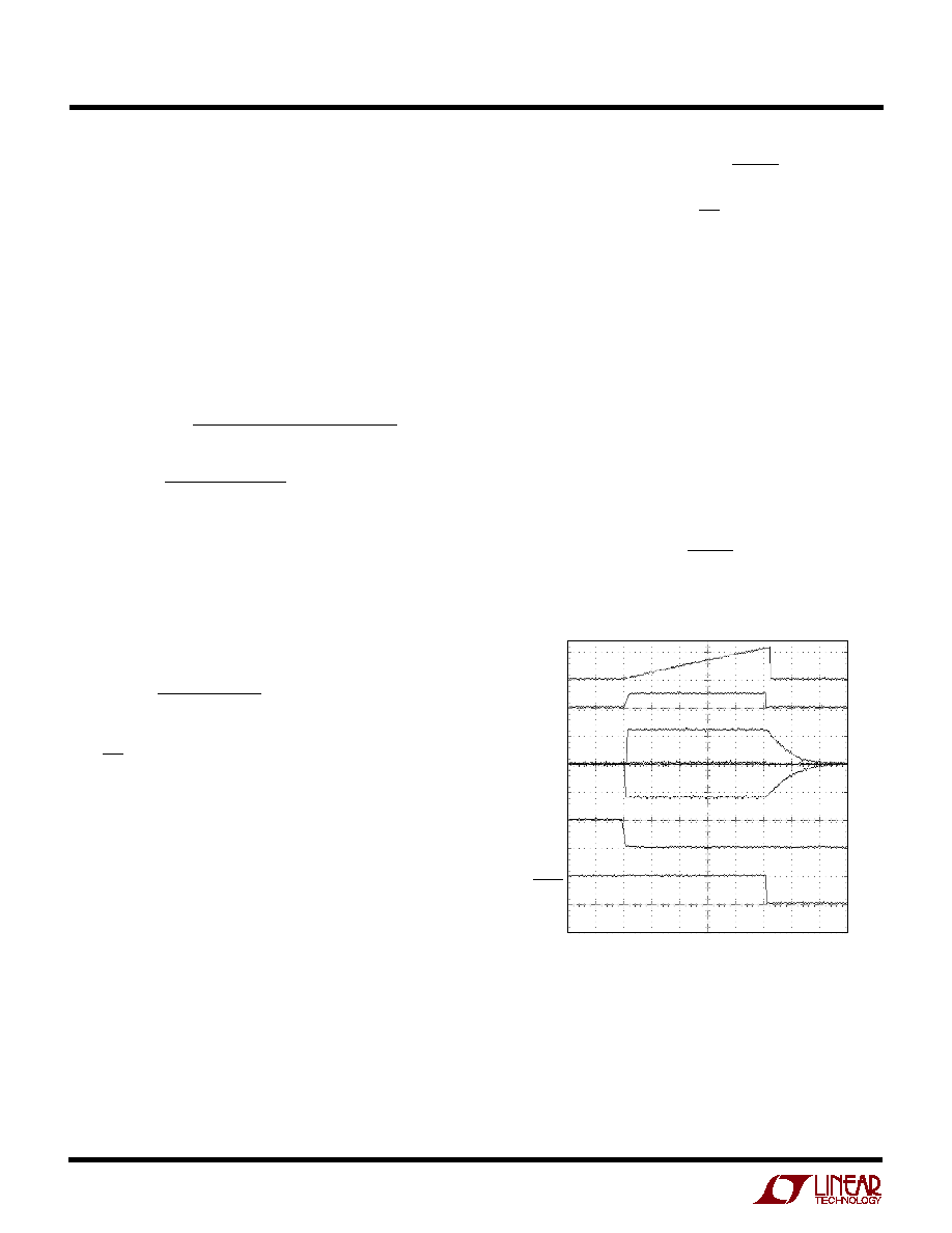
Power-Down Sequence
When either BD_SEL# (OFF/ON) or Bit 2 of the command
latch (C2) is set high, a power-down sequence begins
(Figure 5).
The TIMER pin is immediately pulled low. The GATE pin
(Pin 19) is pulled down by a 200
µ
A current source to
prevent the load currents on the 3.3V and 5V supplies from
going to zero instantaneously and glitching the power
supply voltages. Internal switches are connected to each
of the output supply voltage pins to discharge the output
bulk capacitors to ground. When any one of the output
voltages drops below its PWRGD threshold, the HEALTHY#
signal pulls high, LOCAL_PCI_RST# (RESETOUT) is as-
serted low, and the external status LED turns on.
Once the power-down sequence is complete the status
LED will light up and the CPCI card may be removed from
the slot. During extraction, the precharge circuit will
continue to bias the bus I/O pins at 1V until the long
connector pin connections are broken.
Early Power
Early Power usage is restricted by the CompactPCI (CPCI)
specification. It is intended to power up the precharge
circuit and I/O cells. The CPCI specification allows any of
the long power pins (5V, 3.3V, V(I/O)) to be used for Early
Power. Since Early Power is not isolated, a resistor should
be placed in series with each CPCI connector pin. Note that
if any Early Power pin is shorted on the inserted card, the
current limiting resistor will dissipate the power.
In order to maximize the DC current available from the 5V
supply, all eight 5V connector pins should be tied together
on the inserted card. The same applies to the ten 3.3V CPCI
connector pins. Early Power should then be drawn from
either or both of the two V(I/O) long pins. If either or both
of 5V and 3.3V is used for Early Power, then the 5V and
3.3V sense resistor values must be chosen such that the
1A/pin CPCI rule is not violated.
Connecting V
EEIN
To lessen the likelihood of faulting on power up, the V
EEOUT
output pin should be bypassed with a capacitor that is only
as large as necessary. A value of 10
µ
F to 47
µ
F is recom-
mended. If a large value bypass capacitor is used (e.g.
100
µ
F) on V
EEOUT
, current limit faults may occur during
power-up or during recovery from power failures.
TIMER
10V/DIV
GATE
10V/DIV
12V
OUT
10V/DIV
V
EEOUT
10V/DIV
5V
OUT
10V/DIV
3V
OUT
10V/DIV
LCL_PCI_RST#
5V/DIV
BD_SEL#
5V/DIV
HEALTHY#
5V/DIV
10ms/DIV
4240 F05
Figure 5. Normal Power-Down Sequence
APPLICATIO S I FOR ATIO
W
U
U
U
LTC4240
18
4240f
TIMER
5V/DIV
GATE
5V/DIV
12V
OUT
10V/DIV
V
EEOUT
10V/DIV
5V
OUT
10V/DIV
3V
OUT
10V/DIV
BD_SEL#
5V/DIV
FAULT
5V/DIV
10ms/DIV
4240 F06
Figure 6. Power-Up into a Short on 3.3V Output
Timer
During a power-up sequence, an 11.5
µ
A current source is
connected to the TIMER pin (Pin 5) and charges up the
external TIMER pin capacitor. Current limit faults are
ignored until the TIMER voltage ramps to 5.5V. This feature
allows the LTC4240 to power-up CPCI boards with widely
varying capacitive loads on the back end supplies. The
power-up time for either of the two outputs under current
limit conditions is given by the slower of:
t
XV
C
XV
I
I
or
a
t
GATE
C XV
V
A
b
ON
OUT
LOAD XVOUT
OUT
LIMIT XVOUT
LOAD XVOUT
ON
OUT
TH
(
)
∑
∑
≠
( )
(
)
(
)
( )
(
)
(
)
(
)
=
=
+
µ
2
2
1
65
2
Where XV
OUT
= 5V
OUT
or 3V
OUT
. The timer period should
be set longer than the maximum supply turn-on time but
short enough to not exceed the maximum safe operating
area of the pass transistor during a short-circuit. V
TH
is the
threshold voltage of the external power FET (2V ≠ 3V). The
timer period will be:
t
C
V
A
TIMER
TIMER
=
∑
µ
5 5
11 5
.
.
(3)
The TIMER pin is immediately pulled low when either
OFF/ON (Pin 28) or Bit 2 of command latch (C2) goes high.
The TIMER pin also functions as a temporary auxiliary
supply for 12V
IN
. In the event of a large (greater than 1V)
glitch on 12V
IN
, the energy stored on the timer capacitor
is used as substitute 12V
IN
power. This improves the
glitch immunity of the LTC4240.
Thermal Shutdown
The internal switches for the 12V and ≠12V supplies are
protected by current limit and thermal shutdown circuits.
When the temperature of the die reaches 150
∞
C, all four
switches will be latched off and the FAULT pin (Pin 7) will
be pulled low. Since there is no automatic retry, power will
have to be cycled with the OFF/ON pin or the I
2
C command
latch.
Short-Circuit Protection
In order to lower power dissipation in the pass transistors
and to mitigate voltage spikes on the supplies during
short-circuit conditions, the current limit on each supply
is designed to be a function of the output voltage. As the
output voltage drops, the current limit decreases. Unlike a
traditional circuit breaker function where huge currents
can flow before the breaker trips, the current foldback
feature lowers short-circuit current by at least 50% when
powering up into a short.
If any supply is in current limit after the TIMER pin voltage
has ramped to 5.5V, then all four pass transistors will be
immediately turned off and FAULT will be asserted low
(Figure 6).
APPLICATIO S I FOR ATIO
W
U
U
U
LTC4240
19
4240f
Once the TIMER voltage has reached 5.5V, all of the
supplies will be latched off if any supply enters current
limit for at least 35
µ
s. The 35
µ
s delay prevents quick
current spikes--for example, from a fan turning on--
from causing false trips of the circuit breaker.
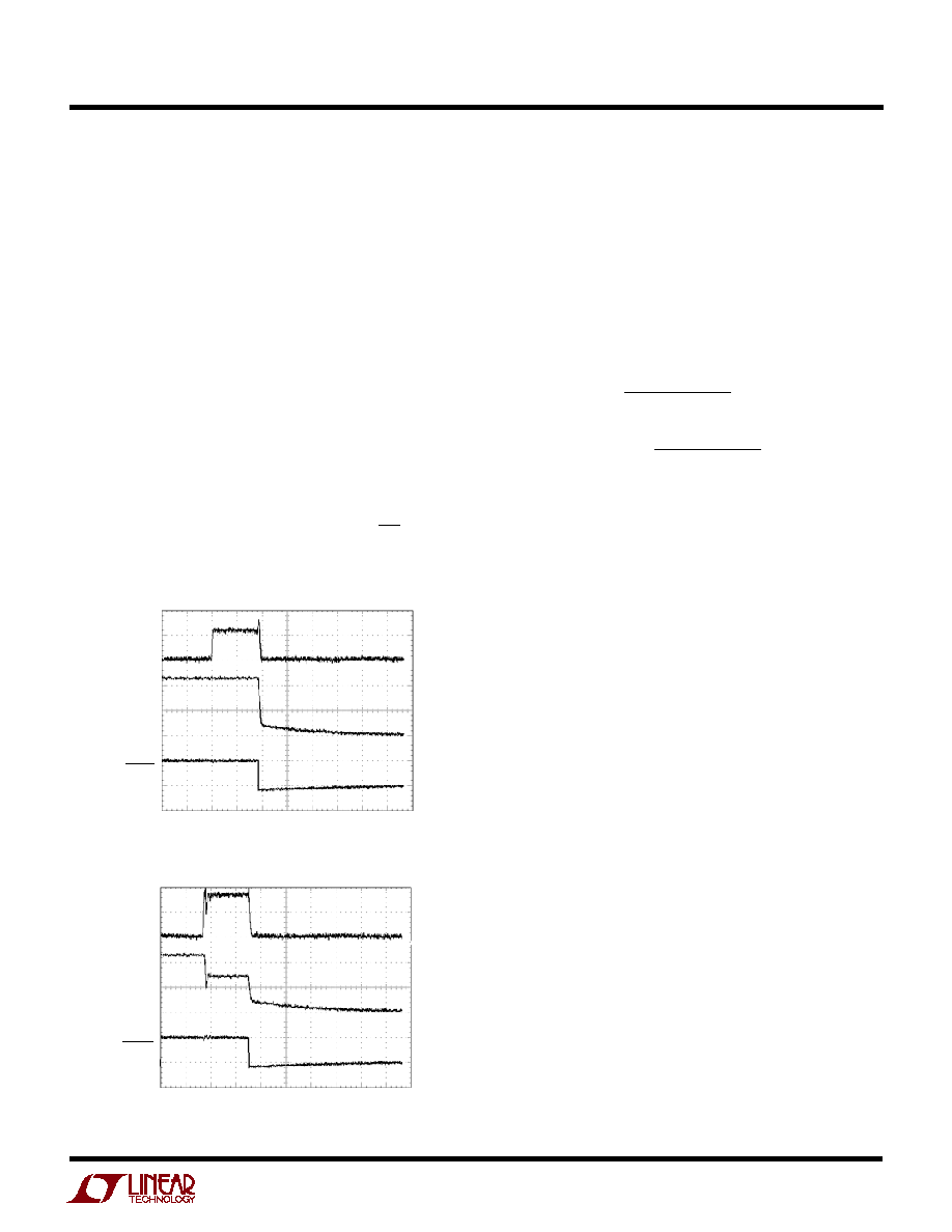
During normal operation, the 5V and 3.3V supplies are
protected from overcurrent and short-circuit conditions
by dual-level circuit breakers. In the event that either
supply current exceeds the nominal limit, an internal timer
is started. If the supply is still overcurrent after 35
µ
s, the
circuit breaker trips and all the supplies are turned off
(Figure 7). If a short-circuit occurs on 5V
OUT
or 3V
OUT
and
the supply current exceeds three times the set limit, an
analog loop will limit the current to 3 times the value set
by R
SENSE
and 55mV. If the short persists for more than
35
µ
s, the LTC4240 latches off (Figure 8). It will stay in the
latched off state until it is reset using the OFF/ON pin or by
using the I
2
C interface. The LTC4240 can also be reset by
cycling any of the power supplies.
The current limit and the foldback current level for the 5V
and 3.3V outputs are both a function of the external sense
resistor (R1 for 3V
OUT
and R2 for 5V
OUT
, see front page).
A sense resistor is connected between 5V
IN
(Pin 21) and
5V
SENSE
(Pin 20) for the 5V supply. For the 3.3V supply, a
sense resistor is connected between 3V
IN
(Pin 22) and
3V
SENSE
(Pin 23). The current limit and the current foldback
current level are given by Equations 4 and 5:
I
mV
R
I
mV
R
LIMIT XVOUT
SENSE XVOUT
FOLDBACK XVOUT
SENSE XVOUT
(
)
(
)
(
)
(
)
( )
( )
=
=
55
4
11
5
where XV
OUT
= 5V
OUT
or 3V
OUT
.
Equation 4 is the current limit for XV
OUT
XV
IN
. Equation
5 shows the I
LIMIT
for shorted outputs. Both equations
assume voltage on TIMER pin is greater than 5.5V.
XV
OUT
= 3V
OUT
or 5V
OUT
. Note that since there are only 8
pins connecting 5V
IN
, R
SENSE
0.007
for 5V
IN
.
The current limit for the internal 12V switch is set at
≠1200mA folding back to ≠350mA and the ≠12V switch at
500mA folding back to 250mA.
Selecting R
SENSE
An equivalent circuit for the 5V and 3.3V circuit breakers
is shown in Figure 9. The sense resistor and the circuit
breaker threshold voltage determine the fault current that
turns off the external FETs. Sense resistors with a 1%
tolerance are recommended. Due to part to part and
temperature variations for both the sense resistor value
and the circuit breaker threshold voltage, the actual cur-
rent limit threshold will exhibit some variation. To calcu-
late the smallest value of current that will trip the fault
comparator, use the largest value of the sense resistor and
the smallest value of the threshold voltage. A 0.005
1%
sense resistor (on the 3.3V supply, for example) with
typical temperature coefficients would increase to ap-
proximately 0.0051
(nominal value multiplied by the 1%
tolerance and the TC at 70
∞
C). Since the minimum value of
the threshold voltage is 50mV, this implies a current limit
of 9.8A. To arrive at the largest value of the current limit
that will turn off the external FETs, the nominal value of the
APPLICATIO S I FOR ATIO
W
U
U
U
Figure 7. Overcurrent Fault on 5V
Figure 8. Short-Circuit Fault on 5V
GATE
5V/DIV
5V
IN
≠5V
SENSE
100mV/DIV
FAULT
5V/DIV
20
µ
s/DIV
4240 F07
GATE
5V/DIV
5V
IN
≠5V
SENSE
100mV/DIV
FAULT
5V/DIV
20
µ
s/DIV
4240 F08
LTC4240
20
4240f
On Resistance
The CompactPCI specification limits the total IR drop of
the FET plus the IR drop of the sense resistor to 100mV.
For a nominal sense resistor of 0.005
, if the user limits
the 3.3V supply load current to 8.7A, then the maximum
FET resistance should be less than 0.0063
. Similarly, for
a 6.2A load current on the 5V supply and a 0.007
sense
resistor, the maximum 5V FET resistance should be
0.0088
. Note that above values of FET resistance are
worst case over temperature (on the FET's datasheet, find
the resistance vs temperature curve and de-rate the room
temperature maximum value).
Breakdown Voltage
The maximum DC voltage that can appear across the
drain/source of the external power FET is 5V +10%. During
transient events and hot swap conditions, parasitic induc-
tances could cause ringing up to 3 times the supply
voltage. The use of voltage transient suppressors at the 5V
and 3.3V inputs can limit these voltage swings to less than
10V (see front page schematic). Similarly, the largest DC
voltage that is likely to appear across the gate is 12V
+10%. Voltage suppressors on the 12V
IN
node will also
limit the transient spikes on that node. Additionally, the
total capacitance on the GATE node will serve to filter fast
voltage noise spikes. FETs with a minimum rating of
±
20V
on both the drain/source and the gate/source are recom-
mended.
Steady State Power Dissipation
For a user selected maximum load current of 8.7A on the
3.3V power supply and a 0.0063
maximum FET resis-
tance, the DC power dissipation is:
(I
MAX
)
2
(R
DSON,MAX
) = (8.7)(8.7)(0.0063) = 0.477W
This is within the SOA limits of most power FETs.
sense resistor drops to 0.0049
and the largest value of
threshold voltage increases to 60mV. This results in a trip
current of 12.2A.
≠
+
+
≠
5V
IN
5V
IN
R
SENSE
5V
SENSE
V
CB
V
CB(MAX)
= 60mV
V
CB(NOM)
= 55mV
V
CB(MIN)
= 50mV
21
20
I
LOAD(MAX)
LTC4240*
*ADDITIONAL DETAILS
OMITTED FOR CLARITY
4240 F09
Figure 9. Circuit Breaker Equivalent
Circuit for Calculating R
SENSE
APPLICATIO S I FOR ATIO
W
U
U
U
Plug-in board designers are thus limited to using less than
9.8A when a nominal 0.005
resistor is used. Using more
than 9.8A runs the risk of turning off the external FET.
Since the CompactPCI specification allows a maximum
1A/pin, at least 10 pins must be used to supply 9.8A. This
implies that only the 3.3V supply can use a 0.005
resistor, since the 5V supply has a maximum of 8 pins
available. To adhere to the 1A/pin specification, the 5V
sense resistor should be larger than the 3.3V sense
resistor. Typical applications show a nominal 0.007
resistor, which results in a 7.04A maximum deliverable
current to the plug-in board loads. The 7.04A current
implies at least 7 pins on the 5V connector. Note that the
thermal considerations of the external FET will also place
limitations on the maximum allowable current.
5V and 3.3V External FET Selection
The LTC4240 uses external power FETs to limit and
modulate the current delivered by the 3.3V and 5V sup-
plies. There are several parameters to consider when
selecting the FET:
1. On resistance.
2. Gate and drain breakdown voltage.
3. Steady state and transient power dissipation.
LTC4240
21
4240f
Transient Power Dissipation
There are certain transient events that can significantly
increase the power dissipated by the external FET. If the
LTC4240 5V supply (at 5V + 10%) powers up into a 1.5V
short (potentially manifested as a short to two diodes in
series), then the FET can potentially have 4V across it with
8.8A flowing. This implies a power dissipation of 35.1W.
The amount of time the FET will dissipate 35.1W will
depend on the relative values of the TIMER and GATE
capacitances. For the values specified on the front page
application circuit, the GATE pin will ramp high signifi-
cantly faster than the TIMER pin, hence transient power
dissipation will be set by the TIMER pin capacitance.
The dissipated 35.1W, the ramp time of the TIMER pin
(50ms will be used for this example), and the FET thermal
resistance will determine the internal junction tempera-
ture of the FET. Most FETs will specify a maximum internal
junction temperature of 150
∞
C. The FET datasheets should
have a transient thermal impedance graph. This graph has
a family of curves listing the FET transient thermal imped-
ance as a function of duty cycle. The duty cycle refers to
what percentage of the time the FET is in the short circuit
condition. If we choose the Si7880DP FET and assume
that the board on which the FET is placed has minimal heat
sinking capability, and further assume that the user will
turn on the board every 2.5 seconds (0.02 duty cycle:
50ms on, 2450ms off), then by looking at the junction-to-
ambient curve we note that with a 70
∞
C ambient tempera-
ture, the Si7880DP internal junction temperature will be
172
∞
C. This is above the absolute maximum rating of the
FET, and although operating at this temperature will not
damage the FET immediately, it does affect its long term
reliability. Conversely, if we assume that there is a perfect
heat sink for the Si7880DP package, then we would use the
junction-to-case curve and calculate a value of 117
∞
C with
a 70
∞
C ambient temperature. The Si7880DP comes in a
thermally enhanced package whose drain lead is a large
piece of metal that can conduct heat away from the internal
junction of the FET. To achieve best performance, the drain
of the Si7880DP should be connected to a piece of copper
(as large as possible) on the board. Note that if the output
is shorted to ground, the current foldback feature will cut
the power dissipation by at least a factor of two.
APPLICATIO S I FOR ATIO
W
U
U
U
When the LTC4240 is turned on and the large 5V
OUT
output capacitor (2000
µ
F or more) is charged, it is pos-
sible that the 5V FET will dissipate as much as the 35.1W
described above. If there is no DC load at 5V
OUT
, then 8.8A
will charge the 2000
µ
F in less than 2ms, which should not
pose any thermal problems for the Si7880DP. If the DC
load at 5V
OUT
approaches the current limit, then the above
analysis should be used to calculate the internal junction
temperature of the FET.
Output Voltage Monitor
The DC level of all four supply outputs is monitored by the
power good circuitry. When any of the four supply outputs
falls below its specified level (see DC electrical specifica-
tions) for longer than 10
µ
s, the PWRGD (HEALTHY#)
open drain pin will be deasserted and the LOCAL_PCI_RST#
signal will be asserted low. This does not generate a fault
condition.
The LOCAL_PCI_RST# signal (RESETOUT pin) is derived
from the HEALTHY# (PWRGD pin), PCI_RST# (RESETIN
pin), and Bit 3 of the command latch (see Table 5).
Table 5. LOCAL_PCI_RST# Truth Table
Bit 3 (C3 )
PCI_RST#
HEALTHY#
Command Latch
LOCAL_PCI_RST#
LO
X
X
LO
X
HI
X
LO
X
X
HI
LO
HI
LO
LO
HI
Precharge
The PRECHARGE input and DRIVE output pins are used to
generate the 1V precharge voltage that biases the bus I/O
connector pins during board insertion and extraction
(Figure 10). The LTC4240 is capable of generating
precharge voltages other than 1V. Figure 11 shows a
circuit that can be used in applications requiring a precharge
voltage less than 1V. The circuit in Figure 12 can be used
for applications that need precharge voltages greater than
1V. Table 6 lists suggested resistor values for R11A and
R11B vs precharge voltage for the application circuits
shown in Figures 11 and 12.
LTC4240
22
4240f
Table 6. R1 and R2 Resistor Values vs Precharge Voltages
V
PRECHARGE
R11A
R11B
V
PRECHARGE
R11A
R11B
1.5V
18
9.09
0.9V
16.2
1.78
1.4V
18
7.15
0.8V
14.7
3.65
1.3V
18
5.36
0.7V
12.1
5.11
1.2V
18
3.65
0.6V
11
7.15
1.1V
18
1.78
0.5V
9.09
9.09
1V
18
0
Figure 12. Precharge Voltage Greater Than 1V
Figure 11. Precharge Voltage Less Than 1V
3V
IN
5V
IN
3V
IN
5V
IN
22
21
LTC4240*
4240 F10
R
I01
10
, 5%
I/O
I/O
R
I0128
10
, 5%
PCI
BRIDGE
(21154)
UP TO 128
I/O LINES
DATA BUS
3V
IN
GND
PRECHARGE
18
DRIVE
17
10
R
PRE1
10k
5%
PRECHARGE OUT
1V
±
20%
I
OUT
=
±
55mA
R11
18
, 5%
R
PRE128
10k
5%
R8
1k, 5%
R7
12
, 5%
C3
4.7nF
R9
24
, 5%
CompactPCI
BACKPLANE
CONNECTOR
(FEMALE)
CompactPCI
BACKPLANE
CONNECTOR
(MALE)
MEDIUM 5V
LONG 5V
3.3V
LONG 3.3V
GROUND
I/O PIN 1
I/O PIN 128
∑ ∑ ∑
∑ ∑ ∑
∑ ∑ ∑
∑ ∑ ∑
R22
2.74
R21
1.74
*ADDITIONAL DETAILS OMITTED FOR CLARITY
Q3
MMBT2222A
Q3
MMBT2222A
C3
4.7nF
R7
12
, 5%
R9
24
, 5%
R8
1k, 5%
3V
IN
PRECHARGE OUT
GND
PRECHARGE
DRIVE
LTC4240*
10
18
17
R11A
R11B
V
PRECHARGE
= ∑ 1V
R11A
R11A + R11B
4240 F11
*ADDITIONAL DETAILS
OMITTED FOR CLARITY
Q3
MMBT2222A
C3
4.7nF
R7
12
, 5%
R9
24
, 5%
R8
1k, 5%
3V
IN
PRECHARGE OUT
GND PRECHARGE
DRIVE
LTC4240*
10
18
17
R11A
R11B
V
PRECHARGE
= ∑ 1V
R11A + R11B
R11A
4240 F12
*ADDITIONAL DETAILS
OMITTED FOR CLARITY
Figure 10. Precharge Application Circuit
Precharge resistors are used to connect the 1V bias
voltage to the CompactPCI connector I/O lines. This allows
live insertion of the I/O lines with minimal disturbance.
Figure 13 shows the precharge application circuit for 5V
signaling environments. The precharge resistor require-
ments are more stringent for 3.3V and Universal Hot Swap
signaling. If the total leakage current on the I/O line is less
APPLICATIO S I FOR ATIO
W
U
U
U
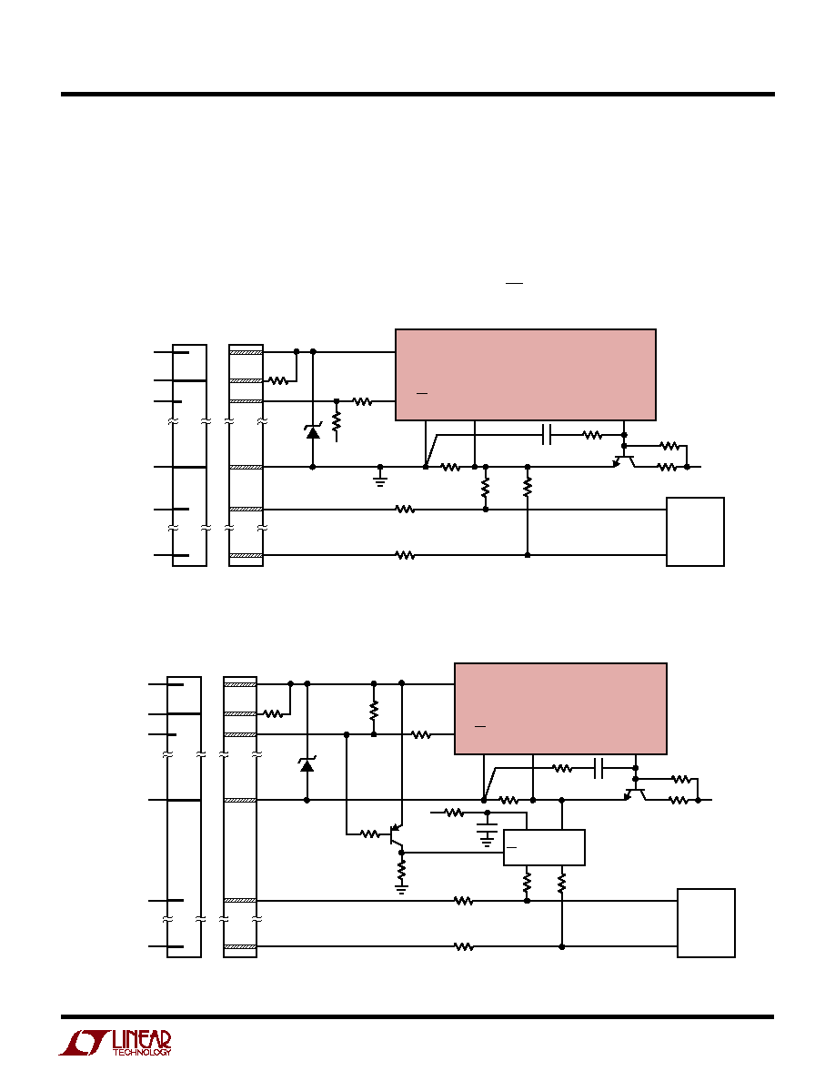
LTC4240
23
4240f
APPLICATIO S I FOR ATIO
W
U
U
U
than 2
µ
A, then a 50K resistor can be connected directly
from the 1V bias voltage to the I/O line. However, many ICs
connected to the I/O lines can have leakage currents up to
10
µ
A. For these applications, a 10k resistor is used but
must be disconnected when the board has been seated as
determined by the state of the BD_SEL# signal. Figure 14
shows a precharge circuit that uses a bus switch to
GND
5V
IN
OFF/ON
5V
IN
LTC4240*
PRECHARGE
DRIVE
21
28
18
17
Z4: 1PMT5.0AT3
*ADDITIONAL DETAILS OMITTED FOR CLARITY
DATA BUS
I/O
4240 F14
Q3
MMBT2222A
10
R11
18
, 5%
R18
1k, 5%
3V
IN
R
I01
10
5%
R
PRE1
10k
5%
R
PRE128
10k
5%
PRECHARGE OUT
1V
±
10%
I
OUT
=
±
55mA
I/O
R
I0128
10
5%
R22
2.74
R8
1k, 5%
R7
12
, 5%
C3, 4.7nF
R9
24
PCI
BRIDGE
CHIP
MEDIUM 5V
LONG 5V
BD_SEL#
GROUND
I/O PIN 1
I/O PIN 128
∑ ∑ ∑
∑ ∑ ∑
∑ ∑ ∑
Z4
UP TO 128 I/O LINES
0.1
µ
F
100
LONG
5V
Q4
MMBT3906
R26
51.1k, 5%
R27
75k
5%
BUS SWITCH
V
DD
OE
OUT
OUT
IN
CompactPCI
BACKPLANE
CONNECTOR
(FEMALE)
CompactPCI
BACKPLANE
CONNECTOR
(MALE)
R17
1.2k
5%
Figure 14. Precharge Bus Switch Application Circuit for 3.3V and Universal Hot Swap Boards
Figure 13.Precharge Application Circuit for 5V Signaling Systems
GND
5V
IN
OFF/ON
5V
IN
LTC4240*
PRECHARGE
DRIVE
21
28
18
17
Z4: 1PMT5.0AT3
*ADDITIONAL DETAILS OMITTED FOR CLARITY
DATA BUS
I/O
4240 F13
PRECHARGE OUT
1V
±
10%
I
OUT
=
±
55mA
R
PRE1
10k
5%
R11
18
, 5%
R18
1k, 5%
3V
IN
R
I01
10
5%
I/O
R
I0128
10
5%
R17
1.2k
5%
R22
2.74
R
PRE128
10k
5%
R8
1k, 5%
R7
12
, 5%
C3, 4.7nF
R9
24
PCI
BRIDGE
CHIP
MEDIUM 5V
LONG 5V
BD_SEL#
GROUND
I/O PIN 1
I/O PIN 128
∑ ∑ ∑
∑ ∑ ∑
∑ ∑ ∑
LONG
5V
Z4
UP TO 128 I/O LINES
Q3
MMBT2222A
CompactPCI
BACKPLANE
CONNECTOR
(FEMALE)
CompactPCI
BACKPLANE
CONNECTOR
(MALE)
connect the individual 10k precharge resistors to the
LTC4240 1V PRECHARGE pin. The electrical connection is
made (bus switches close) when the voltage on the
BD_SEL# pin of the plug-in card is above 4.4V, which
occurs just after the long pins have made contact. The bus
switches are subsequently electrically disconnected when
the board connector makes contact with the BD_SEL# pin
(bus switch OE pin is pulled high by Q4).
LTC4240
24
4240f
PRSNT1#
PRSNT2#
Expansion Configuration
Open
Open
No plug in board present
Ground
10k Pull-Up
Plug-in board present,
maximum power consumption
10k Pull-Up
Ground
Plug-in board present,
nominal power consumption
Ground
Ground
Plug-in board present,
minimum power consumption
Other CompactPCI Applications
If no 3.3V supply input is required, Figure 15 illustrates
how the LTC4240 should be configured.
For applications where the BD_SEL# connector pin is
grounded on the backplane, the circuit in Figure 16 allows
the LTC4240 to be reset simply by pressing a pushbutton
switch on the CPCI plug-in board. This arrangement
allows for manual resetting of the LTC4240's circuit break-
ers.
Input Transient Protection
Hot-plugging a board into a backplane generates inrush
currents from the backplane power supplies. This is due to
the charging of the plug-in board bulk capacitance. To
reduce this transient current to a safe level, the CPCI Hot
Swap specification restricts the amount of unswitched
capacitance used on the input side of the plug-in board.
Each pin connected to the CPCI female connector on the
plug-in board is allowed at most 0.01
µ
F/pin. Bulk capaci-
tors are only allowed on the switched output side of the
LTC4240 (5V
OUT
, 3V
OUT
, 12V
OUT
, V
EEOUT
). Some bulk
capacitance is allowed on the Early Power planes, but only
because a current limiting resistor is assumed to separate
the connector from the bulk capacitor. Circuits normally
placed on the unswitched Early Power (PCI Bridge, for
example) need to have a current limiting resistor.
APPLICATIO S I FOR ATIO
W
U
U
U
The assumption by the CompactPCI specification is that
there is a diode to 3.3V on the circuit that is driving the
BD_SEL# pin. The 1.2k resistor pull up to 5V
IN
on the plug-
in card will thus be clamped by the diode to 3.3V. If the
BD_SEL# pin is being driven high, the actual voltage on the
pin will be approximately 3.9V. This is still above the high
TTL threshold of the LTC4240 OFF/ON pin, but low enough
for Q4 to disable the bus switches and thus remove the 10k
resistors from the I/O lines. Note that BD_SEL# is ordi-
narily connected to V(I/O), which in turn is allowed to be
driven by either 3.3V or 5V. For applications such as
shown in Figure 14, the pull up on BD_SEL# is restricted
to the long 5V pins. A bus switch with no internal diode to
V
DD
is preferred. Since the power to the bus switch is
derived from one of the unswitched power planes, a 100
resistor plus a 0.1
µ
F bypass capacitor should be placed in
series with its power supply.
When the plug-in card is removed from the connector, the
BD_SEL# connection is broken first, and the BD_SEL#
voltage pulls up to 5V. This causes Q4 to turn off, which re-
enables the bus switch, and the precharge resistors are
again connected to the LTC4240 PRECHARGE pin for the
remainder of the board extraction process.
The LTC4240 BE pin can alternatively be used to drive the
enable input of the bus switch. The BE signal would then
keep the I/O lines precharged until all supplies reached
power good status. The resistor in series with the
PRECHARGE pin protects the internal circuitry from large
voltage transients during live insertion.
PRSNT1#, PRSNT2#
PRSNT1# and PRSNT2# are PCI signals that convey the
plug-in board's power consumption information. These
pins should either be shorted to ground or be connected
to Early Power with a 10k resistor. The voltage levels (TTL)
at the PRSNT#1, 2 pins can be read using the I
2
C 2-wire
interface.
LTC4240
25
4240f
Disallowing bulk capacitors on the input power pins
mitigates the inrush current during hot plug. However, it
also tends to create a resonant circuit formed by the
inductance of the backplane power supply trace and the
parasitic capacitance of the plug-in board (mainly due to
the large power FET). Upon board insertion, the ringing of
this circuit will exhibit peak overshoot as high as 2.5 times
the steady state voltage (>30V for 12V).
There are two methods for abating the effects of these high
voltage transients: using zener clamps, and using snubber
APPLICATIO S I FOR ATIO
W
U
U
U
Figure 17. Place Transient Protection Device Close to the LTC4240
C1
0.047
µ
F
C7
0.1
µ
F
0.1
µ
F
3V
IN
MEDIUM 3.3V
MEDIUM 5V
3V
SENSE
22
3V
OUT
24
5V
IN
21
5V
OUT
6
5V
SENSE
20
23
GATE
19
R3
10
R4
10
5V
OUT
AT 5A
3V
OUT
AT 7.6A
R5
1k
R1
0.005
Q1
Si7880DP
Q2
Si7880DP
R2
0.007
Z3
Z4
LTC4240*
1644 F17
GND
10
Z3, Z4: 1PMT5.0AT3
*ADDITIONAL DETAILS OMITTED FOR CLARITY
LONG 5V
LONG 3.3V
2.7
R23
2.7
R22, 2.74
R21, 1.74
Figure 15. 5V Supply Only Application Circuit
MEDIUM 5V
LONG
5V
C1
0.047
µ
F
GND
21
3V
OUT
6
LTC4240*
22
5V
OUT
24
23
20
GATE
19
10
4240 F15
R5
1k
R22
2.74
CompactPCI
BACKPLANE
CONNECTOR
(FEMALE)
CompactPCI
BACKPLANE
CONNECTOR
(MALE)
GND
5V
IN
5V
IN
D1
5V
SENSE
3V
IN
3V
SENSE
R4
10
5V
OUT
R2
0.007
Q2
Si7880DP
D2
D1, D2: BAV99
C
L(5VOUT)
Z4
*ADDITIONAL DETAILS OMITTED FOR CLARITY
Z4: 1PMT5.0AT3
GND
LTC4240*
10
1.2k
PUSHBUTTON
SWITICH
100
V(I/O)
1k
GND
OFF/ON
28
BD_SEL#
4240 F16
*ADDITIONAL DETAILS OMITTED FOR CLARITY
CompactPCI
BACKPLANE
CONNECTOR
(FEMALE)
CompactPCI
BACKPLANE
CONNECTOR
(MALE)
Figure 16. BD_SEL# Pushbutton Toggle Switch
networks. Snubbers are RC networks whose time
constants are large enough to damp the inductance of the
parasitic resonant circuit. The snubber capacitor should
be 10X to 100X the value of the plug-in board parasitic
capacitance. The value of the series snubber resistor
should be large enough to damp the resulting
R-L-C circuit and is typically between 1
and 50
. These
protection networks should be mounted very close to the
LTC4240 in order to minimize parasitic inductance. This is
shown in Figure 17 for the 3.3V and 5V supplies.
LTC4240
26
4240f
CURRENT FLOW
TO SOURCE
*ADDITIONAL DETAILS OMITTED FOR CLARITY. DRAWING IS NOT TO SCALE!
4240 F18
TRACK WIDTH W:
0.03" PER AMPERE
ON 1OZ Cu FOIL
D
D
D
D
G
S
S
S
CURRENT FLOW
TO LOAD
CURRENT FLOW
TO LOAD
SENSE
RESISTOR
VIA TO
GND PLANE
GND
GND
5V
OUT
5V
5V
IN
5V
VIA/PATH
TO GND
GATE
R4
R5
C1
C
TIMER
W
W
W
POWER
MOSFET
LTC4240CGN*
1
2
3
4
5
6
7
8
9
10
11
12
13
14
28
27
26
25
24
23
22
21
20
19
18
17
16
15
SIMILAR LAYOUT
FOR 3.3V RAIL
NOT SHOWN
Note (see front page schematic) that the 12V and ≠12V
show 0.01
µ
F snubber capacitors. This is consistent with
the CPCI specification since we also recommend a 10
snubber resistor. The 12V
IN
pin is the most sensitive to
high energy large voltage transients. A transient voltage
suppressor with a breakdown voltage between 13.2V and
15V is advisable. The TVS should also be able to dissipate
at least 150W. The SMAJ12CA can be used for both 12V
IN
and V
EEIN
. Place the TVS close to the LTC4240. See front
page schematic.
Figure 18. Recommended Layout for Power MOSFET,
Sense Resistor and GATE Components for the 5V Rail.
Similar Layout for 3.3V Rail Not Shown
APPLICATIO S I FOR ATIO
W
U
U
U
PCB Layout Considerations
For proper operation of the LTC4240's circuit breaker
function, a 4-wire Kelvin connection to the sense resistors
is highly recommended. A recommended PCB layout for
the sense resistor, the power MOSFET, and the GATE drive
components around the LTC4240 is illustrated in
Figure 18. The drawing is not to scale and is only intended
to show the low resistance, external high current path. In
hot swap applications where load currents can reach 10A,
narrow PCB tracks exhibit more resistance than wider
tracks and operate at more elevated temperatures. Since
the sheet resistance of 1 ounce copper is approximately
0.5m
/square, track resistances add up quickly in high-
current applications. Thus, to keep PCB track resistance
and temperature rise to a minimum, the suggested trace
width in these applications for 1 ounce copper is 0.03" for
each ampere of DC current.
In order to help dissipate the heat generated by the power
MOSFET, the copper trace connected to the drain should
be made as large as possible.
In the majority of applications, it will be necessary to use
plated-through vias to make circuit connections from
component layers to power and ground layers internal to
the PC board. For 1 ounce copper plating, a general rule is
1A of DC current per via, making sure the via is properly
dimensioned so that solder completely fills any void. For
other plating thicknesses, check with your PCB fabrication
facility.
Power MOSFET and Sense Resistor Selection
Table 7 lists some current MOSFET transistors that are
available. Table 8 lists some current sense resistors that
can be used with the LTC4240's circuit breakers. Table 9
lists supplier web site addresses for discrete components
mentioned throughout the LTC4240 data sheet. High
current applications should select a MOSFET with very
low on-resistance and good transient thermal character-
istics.
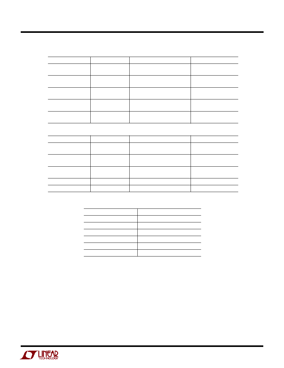
LTC4240
27
4240f
Table 7. N-Channel Power MOSFET Selection Guide
CURRENT LEVEL (A)
PART NUMBER
DESCRIPTION
MANUFACTURER
0 to 2
MMDF3N02HD
Dual N-Channel SO-8
ON Semiconductor
R
DS(ON)
= 0.1
2 to 5
MMSF5N02HD
Single N-Channel SO-8
ON Semiconductor
R
DS(ON)
= 0.025
5 to 10
MTB50N06V
Single N-Channel DD-Pak
ON Semiconductor
R
DS(ON)
= 0.028
5 to 10
IRF7457
Single N-Channel SO-8
International Rectifier
R
DS(ON)
= 0.007
5 to 10
Si7880DP
Single N-Channel PowerPAK
TM
Vishay-Siliconix
R
DS(ON)
= 0.003
Table 8. Sense Resistor Selection Guide
CURRENT LIMIT VALUE
PART NUMBER
DESCRIPTION
MANUFACTURER
1A
LR120601R055F
0.055
, 0.5W, 1% Resistor
IRC-TT
WSL1206R055
Vishay-Dale
2A
LR120601R028F
0.028
, 0.5W, 1% Resistor
IRC-TT
WSL1206R028
Vishay-Dale
5A
LR120601R011F
0.011
, 0.5W, 1% Resistor
IRC-TT
WSL2010R011
Vishay-Dale
7.9A
WSL2512R007
0.007
, 1W, 1% Resistor
Vishay-Dale
11A
WSL2512R005
0.005
, 1W, 1% Resistor
Vishay-Dale
PowerPAK is a trademark of Vishay-Siliconix
APPLICATIO S I FOR ATIO
W
U
U
U
Table 9. Manufacturers' Web Site
MANUFACTURER
WEB SITE
International Rectifier
www.irf.com
ON Semiconductor
www.onsemi.com
IRC-TT
www.irctt.com
Vishay-Dale
www.vishay.com
Vishay-Siliconix
www.vishay.com
Diodes, Inc.
www.diodes.com
Information furnished by Linear Technology Corporation is believed to be accurate and reliable.
However, no responsibility is assumed for its use. Linear Technology Corporation makes no represen-
tation that the interconnection of its circuits as described herein will not infringe on existing patent rights.
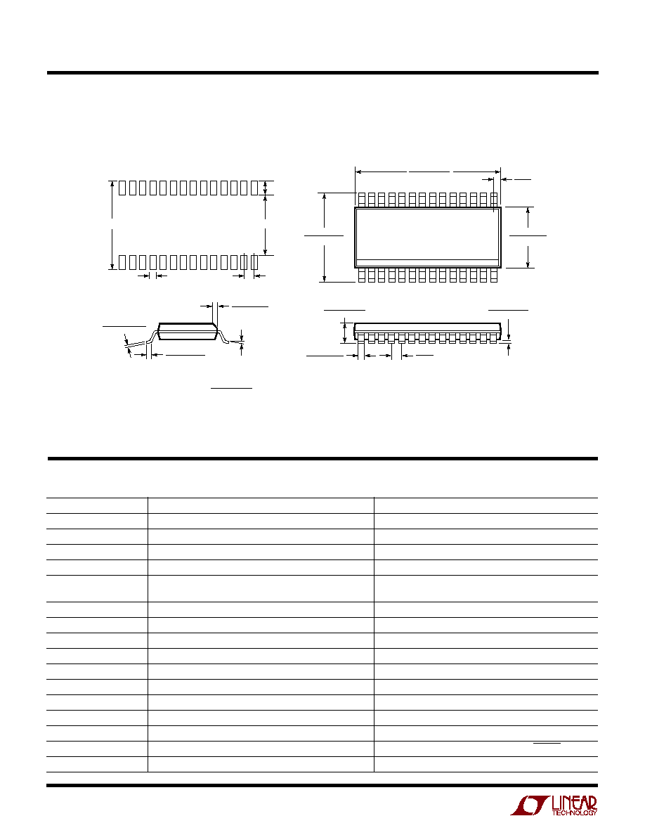
LTC4240
28
4240f
Linear Technology Corporation
1630 McCarthy Blvd., Milpitas, CA 95035-7417
(408) 432-1900
q
FAX: (408) 434-0507
q
www.linear.com
RELATED PARTS
PART NUMBER
DESCRIPTION
COMMENTS
LTC1421
Hot Swap Controller
Dual Supplies for 3V to 12V, Additionally ≠12V
LTC1422
Hot Swap Controller in SO-8
Single Supply from 3V to 12V
LT1641-1/LT1641-2
Positive Voltage Hot Swap Controller in SO-8
Supplies from 9V to 80V, Latched Off/Auto Retry
LTC1642
Fault Protected Hot Swap Controller
3V to 15V, Overvoltage Protection Up to 33V
LTC1643AL/LTC1643AL-1/ PCI Bus Hot Swap Controllers
3.3V, 5V, 12V, ≠12V Supplies for PCI Bus
LTC1643AH
LTC1644
CompactPCI Hot Swap Controller
3.3V, 5V,
±
12V, I/O Precharge and Local Reset Logic
LTC1645
2-Channel Hot Swap Controller
Operates from 1.2V to 12V, Power Sequencing
LTC1646
CompactPCI Hot Swap Controller for 3.3V and 5V
3.3V and 5V only, I/O Precharge and Local Reset Logic
LTC1647
Dual Hot Swap Controller
Dual ON Pins for Supplies from 3V to 15V
LTC4211
Single Hot Swap Controller with Multifunction Current Control 2.5V to 16.5V, Dual Level Circuit Breaker, No Gate Capacitor
LTC4230
Triple Hot Swap Controller with Multifunction Current Control
1.7V to 16.5V, Dual Level Circuit Breaker, No Gate Capacitor
LTC4241
PCI Hot Swap Controller with 3.3V Auxiliary
3.3V, 5V,
±
12V and 3.3VAux Supplies for PCI Bus
LT4250L/LT4250H
≠48 Hot Swap Controllers in SO-8
Active Current Limiting, Supplies from ≠20V to ≠80V
LTC4251
≠48 Hot Swap Controller in SOT-23
Floating Topology, Active Current Limiting
LTC4252
≠48 Hot Swap Controller in MSOP
Floating Topology, Active Current Limiting, PWRGD Output
LTC4350
Hot Swappable Load Share Controller
Eliminates ORing Diodes, Identifies and Localizes Faults
PACKAGE DESCRIPTIO
U
GN Package
28-Lead Plastic SSOP (Narrow .150 Inch)
(Reference LTC DWG # 05-08-1641)
©
LINEAR TECHNOLOGY CORPORATION 2003
LT/TP 0403 2K ∑ PRINTED IN USA
.386 ≠ .393*
(9.804 ≠ 9.982)
GN28 (SSOP) 0502
1
2
3
4
5
6
7
8
9 10 11 12
.229 ≠ .244
(5.817 ≠ 6.198)
.150 ≠ .157**
(3.810 ≠ 3.988)
20
21
22
23
24
25
26
27
28
19 18 17
13 14
1615
.016 ≠ .050
(0.406 ≠ 1.270)
.015
±
.004
(0.38
±
0.10)
◊
45
∞
0
∞
≠ 8
∞
TYP
.0075 ≠ .0098
(0.191 ≠ 0.249)
.053 ≠ .069
(1.351 ≠ 1.748)
.008 ≠ .012
(0.203 ≠ 0.305)
.004 ≠ .009
(0.102 ≠ 0.249)
.0250
(0.635)
BSC
.033
(0.838)
REF
.254 MIN
RECOMMENDED SOLDER PAD LAYOUT
.150 ≠ .165
.0250 TYP
.0165
±
.0015
.045
±
.005
*DIMENSION DOES NOT INCLUDE MOLD FLASH. MOLD FLASH
SHALL NOT EXCEED 0.006" (0.152mm) PER SIDE
**DIMENSION DOES NOT INCLUDE INTERLEAD FLASH. INTERLEAD
FLASH SHALL NOT EXCEED 0.010" (0.254mm) PER SIDE
INCHES
(MILLIMETERS)
NOTE:
1. CONTROLLING DIMENSION: INCHES
2. DIMENSIONS ARE IN
3. DRAWING NOT TO SCALE