 | –≠–ª–µ–∫—Ç—Ä–æ–Ω–Ω—ã–π –∫–æ–º–ø–æ–Ω–µ–Ω—Ç: LTC4252-2 | –°–∫–∞—á–∞—Ç—å:  PDF PDF  ZIP ZIP |
LTC4252-1/LTC4252-2
1
425212f
The LTC
Æ
4252 negative voltage Hot Swap
TM
controller
allows a board to be safely inserted and removed from a
live backplane. Output current is controlled by three stages
of current limiting: a timed circuit breaker, active current
limiting and a fast feedforward path that limits peak
current under worst-case catastrophic fault conditions.
Programmable undervoltage and overvoltage detectors
disconnect the load whenever the input supply exceeds
the desired operating range. The LTC4252's supply input
is shunt regulated, allowing safe operation with very high
supply voltages. A multifunction timer delays initial start-
up and controls the circuit breaker's response time. The
circuit breaker's response time is accelerated by sensing
excessive MOSFET drain voltage, keeping the MOSFET
within its safe operating area (SOA). A programmable
soft-start circuit controls MOSFET inrush current at start-
up. A power good status output can enable a power
module at start-up or disable it if the circuit breaker trips.
The LTC4252-1 latches off after a circuit breaker fault times
out. The LTC4252-2 provides automatic retry after a fault.
The LTC4252 is available in either an 8-pin or 10-pin MSOP.
s
Hot Board Insertion
s
Electronic Circuit Breaker
s
≠ 48V Distributed Power Systems
s
Negative Power Supply Control
s
Central Office Switching
s
Programmable Current Limiting Circuit
s
High Availability Servers
s
Disk Arrays
, LTC and LT are registered trademarks of Linear Technology Corporation.
s
Allows Safe Board Insertion and Removal from a
Live ≠ 48V Backplane
s
Floating Topology Permits Very High Voltage
Operation
s
Programmable Analog Current Limit With Circuit
Breaker Timer
s
Fast Response Time Limits Peak Fault Current
s
Programmable Soft-Start Current Limit
s
Programmable Timer with Drain Voltage
Accelerated Response
s
Programmable Undervoltage/Overvoltage Protection
s
LTC4252-1: Latch Off After Fault
s
LTC4252-2: Automatic Retry After Fault
Negative Voltage
Hot Swap Controllers
Hot Swap is a trademark of Linear Technology Corporation.
≠ 48V/2.5A Hot Swap Controller
4252-1/2 TA01
GND
OV
UV
V
EE
V
IN
SENSE
SS
TIMER
GATE
PWRGD
DRAIN
LTC4252-1
R1
402k
1%
R2
32.4k
1%
C
T
0.33
µ
F
C
SS
68nF
C
C
18nF
≠48V
R
S
0.02
Q1
IRF530S
V
OUT
R
C
10
R3
5.1k
R
IN
3
◊
1.8k IN SERIES
1/4W EACH
1
8
9
10
3
2
7
6
4
5
C1
10nF
C
IN
1
µ
F
C
L
100
µ
F
GND
(SHORT PIN)
+
R
D
1M
LOAD
EN
*
* M0C207
4252-1/2 TA01a
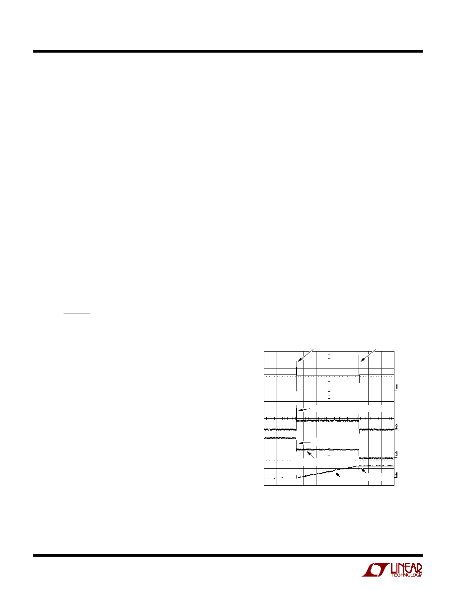
GATE
5V/DIV
SENSE
2.5A/DIV
PWRGD
10V/DIV
1ms/DIV
V
OUT
20V/DIV
Start-Up Behavior
FEATURES
DESCRIPTIO
U
APPLICATIO S
U
TYPICAL APPLICATIO
U
LTC4252-1/LTC4252-2
2
425212f
SYMBOL
PARAMETER
CONDITIONS
MIN
TYP
MAX
UNITS
V
Z
V
IN
≠ V
EE
Zener Voltage
I
IN
= 2mA
q
12
13
14.5
V
r
Z
V
IN
≠ V
EE
Zener Dynamic Impedance
I
IN
= 2mA to 30mA
5
I
IN
V
IN
Supply Current
UV = OV = 4V, V
IN
= (V
Z
≠ 0.3V)
q
0.8
2
mA
V
LKO
V
IN
Undervoltage Lockout
Coming Out of UVLO (Rising V
IN
)
q
9.2
12
V
V
LKH
V
IN
Undervoltage Lockout Hysteresis
1
V
V
CB
Circuit Breaker Current Limit Voltage
V
CB
= (V
SENSE
≠ V
EE
)
q
40
50
60
mV
V
ACL
Analog Current Limit Voltage
V
ACL
= (V
SENSE
≠ V
EE
), SS = Open or 2.2V
q
80
100
120
mV
V
FCL
Fast Current Limit Voltage
V
FCL
= (V
SENSE
≠ V
EE
)
q
150
200
300
mV
V
SS
SS Voltage
After End of SS Timing Cycle
2.2
V
R
SS
SS Output Impedance
100
k
I
SS
SS Pin Current
UV = OV = 4V, V
SENSE
= V
EE
, V
SS
= 0V (Sourcing)
22
µ
A
UV = OV = 0V, V
SENSE
= V
EE
, V
SS
= 2V (Sinking)
28
mA
V
OS
Analog Current Limit Offset Voltage
10
mV
V
ACL
+V
OS
Ratio (V
ACL
+ V
OS
) to SS Voltage
0.05
V/V
V
SS
Current into V
IN
(100
µ
s Pulse) ........................... 100mA
V
IN
, DRAIN Pin Minimum Voltage ....................... ≠ 0.3V
Input/Output Pins
(Except SENSE and DRAIN) Voltage ..........≠ 0.3V to 16V
SENSE Pin Voltage ................................... ≠ 0.6V to 16V
Current Out of SENSE Pin (20
µ
s Pulse) ........... ≠ 200mA
Current into DRAIN Pin (100
µ
s Pulse) ................. 20mA
ORDER PART
NUMBER
MS PART MARKING
T
JMAX
= 125
∞
C,
JA
= 160
∞
C/W
Consult LTC Marketing for parts specified with wider operating temperature ranges.
LTWN
LTWQ
LTRS
LTRT
LTC4252-1CMS
LTC4252-2CMS
LTC4252-1IMS
LTC4252-2IMS
ABSOLUTE AXI U
RATI GS
W
W
W
U
PACKAGE/ORDER I FOR ATIO
U
U
W
All Voltages Referred to V
EE
(Note 1)
ELECTRICAL CHARACTERISTICS
The
q
denotes the specifications which apply over the full operating
temperature range, otherwise specifications are at T
A
= 25
∞
C. (Note 2)
Maximum Junction Temperature .......................... 125
∞
C
Operating Temperature Range
LTC4252-1C/LTC4252-2C ....................... 0
∞
C to 70
∞
C
LTC4252-1I/LTC4252-2I ................... ≠ 40
∞
C to 85
∞
C
Storage Temperature Range ................. ≠ 65
∞
C to 150
∞
C
Lead Temperature (Soldering, 10 sec).................. 300
∞
C
T
JMAX
= 125
∞
C,
JA
= 160
∞
C/W
ORDER PART
NUMBER
MS8 PART MARKING
LTWM
LTWP
LTRQ
LTRR
LTC4252-1CMS8
LTC4252-2CMS8
LTC4252-1IMS8
LTC4252-2IMS8
1
2
3
4
5
V
IN
PWRGD
SS
SENSE
V
EE
10
9
8
7
6
TIMER
UV
OV
DRAIN
GATE
TOP VIEW
MS PACKAGE
10-LEAD PLASTIC MSOP
1
2
3
4
8
7
6
5
TOP VIEW
MS8 PACKAGE
8-LEAD PLASTIC MSOP
V
IN
SS
SENSE
V
EE
TIMER
UV/OV
DRAIN
GATE
LTC4252-1/LTC4252-2
3
425212f
ELECTRICAL CHARACTERISTICS
The
q
denotes the specifications which apply over the full operating
temperature range, otherwise specifications are at T
A
= 25
∞
C. (Note 2)
SYMBOL
PARAMETER
CONDITIONS
MIN
TYP
MAX
UNITS
I
GATE
GATE Pin Output Current
UV = OV = 4V, V
SENSE
= V
EE
,
q
40
58
80
µ
A
V
GATE
= 0V (Sourcing)
UV = OV = 4V, V
SENSE
≠ V
EE
= 0.15V,
17
mA
V
GATE
= 3V (Sinking)
UV = OV = 4V, V
SENSE
≠ V
EE
= 0.3V,
190
mA
V
GATE
= 1V (Sinking)
V
GATE
External MOSFET Gate Drive
V
GATE
≠ V
EE
, I
IN
= 2mA
q
10
12
V
Z
V
V
GATEH
Gate High Threshold
V
GATEH
= V
IN
≠ V
GATE
, I
IN
= 2mA,
2.8
V
for PWRGD Status (MS Only)
V
GATEL
Gate Low Threshold
(Before Gate Ramp-Up)
0.5
V
V
UVHI
UV Pin Threshold HIGH
q
3.075
3.225
3.375
V
V
UVLO
UV Pin Threshold LOW
q
2.775
2.925
3.075
V
V
UVHST
UV Pin Hysteresis
0.3
V
V
OVHI
OV Pin Threshold HIGH
q
5.85
6.15
6.45
V
V
OVLO
OV Pin Threshold LOW
q
5.25
5.55
5.85
V
V
OVHST
OV Pin Hysteresis
0.6
V
I
SENSE
SENSE Pin Input Current
UV = OV = 4V, V
SENSE
= 50mV
q
≠30
≠15
µ
A
I
INP
UV, OV Pin Input Current
UV = OV = 4V
q
±
0.1
±
10
µ
A
V
TMRH
TIMER Pin Voltage High Threshold
4
V
V
TMRL
TIMER Pin Voltage Low Threshold
1
V
I
TMR
TIMER Pin Current
Timer On (Initial Cycle/Latchoff/
5.8
µ
A
Shutdown Cooling, Sourcing), V
TMR
= 2V
Timer Off (Initial Cycle, Sinking), V
TMR
= 2V
28
mA
Timer On (Circuit Breaker, Sourcing,
230
µ
A
I
DRN
= 0
µ
A), V
TMR
= 2V
Timer On (Circuit Breaker, Sourcing,
630
µ
A
I
DRN
= 50
µ
A), V
TMR
= 2V
Timer Off (Circuit Breaker/
5.8
µ
A
Shutdown Cooling, Sinking), V
TMR
= 2V
I
TMRACC
[(I
TMR
at I
DRN
= 50
µ
A) ≠ (I
TMR
at I
DRN
= 0
µ
A)]
Timer On (Circuit Breaker with I
DRN
= 50
µ
A)
8
µ
A/
µ
A
I
DRN
50
µ
A
V
DRNL
DRAIN Pin Voltage Low Threshold
For PWRGD Status (MS Only)
2.385
V
I
DRNL
DRAIN Leakage Current
V
DRAIN
= 5V
±
0.1
±
1
µ
A
V
DRNCL
DRAIN Pin Clamp Voltage
I
DRN
= 50
µ
A
7
V
V
PGL
PWRGD Output Low Voltage
I
PG
= 1.6mA (MS Only)
q
0.2
0.4
V
I
PG
= 5mA (MS Only)
q
1.1
V
I
PGH
PWRGD Pull-Up Current
V
PWRGD
= 0V (Sourcing) (MS Only)
q
40
58
80
µ
A
t
SS
SS Default Ramp Period
SS pin floating, V
SS
ramps from 0.2V to 2V
180
µ
s
t
PLLUG
UV Low to Gate Low
0.4
µ
s
t
PHLOG
OV High to Gate Low
0.4
µ
s
Note 1: Absolute Maximum Ratings are those values beyond which the life
of a device may be impaired.
Note 2: All currents into device pins are positive; all currents out of device
pins are negative. All voltages are referenced to V
EE
unless otherwise
specified.
LTC4252-1/LTC4252-2
4
425212f
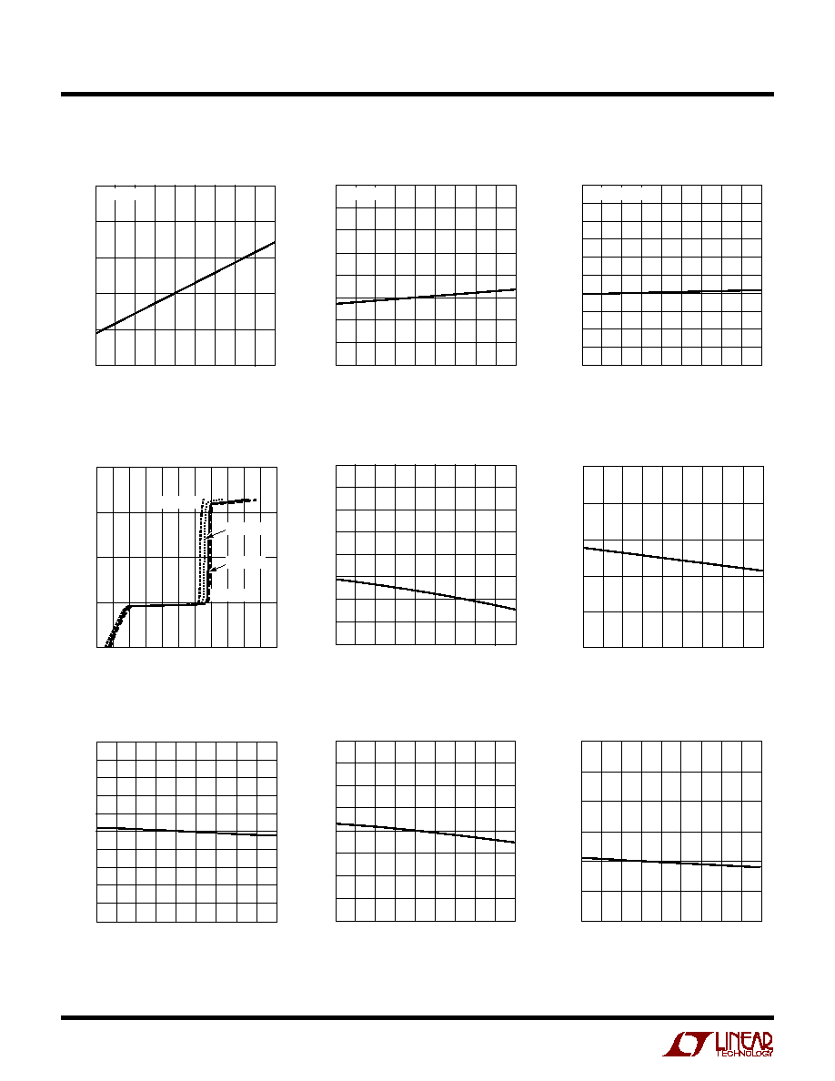
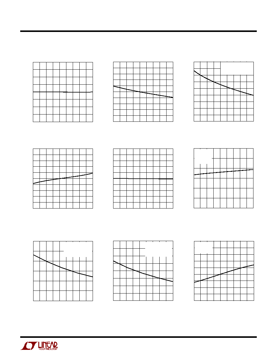
TYPICAL PERFOR A CE CHARACTERISTICS
U
W
I
IN
vs Temperature
r
Z
vs Temperature
V
Z
vs Temperature
Undervoltage Lockout V
LKO
vs Temperature
Undervoltage Lockout Hysteresis
V
LKH
vs Temperature
Circuit Breaker Current Limit
Voltage V
CB
vs Temperature
Analog Current Limit Voltage
V
ACL
vs Temperature
Fast Current Limit Voltage V
FCL
vs Temperature
TEMPERATURE (
∞
C)
≠55
I
IN
(
µ
A)
2000
1800
1600
1400
1200
1000
800
600
400
200
0
≠15
25
45
125
4252-1/2 G01
≠35
5
65
85 105
V
IN
= (V
Z
≠ 0.3V)
V
IN
(V)
0
2
4
6
8
10 12 14 16 18 20 22
I
IN
(mA)
1000
100
10
1
0.1
4252-1/2
G02
T
A
= ≠40
∞
C
T
A
= 125
∞
C
T
A
= 85
∞
C
T
A
= 25
∞
C
TEMPERATURE (
∞
C)
≠55
r
Z
(
)
10
9
8
7
6
5
4
3
2
≠15
25
45
125
4252-1/2 G03
≠35
5
65
85 105
I
IN
= 2mA
TEMPERATURE (
∞
C)
≠55
V
Z
(V)
14.5
14.0
13.5
13.0
12.5
12.0
≠15
25
45
125
4252-1/2 G04
≠35
5
65
85 105
I
IN
= 2mA
TEMPERATURE (
∞
C)
≠55
V
LKO
(V)
12.0
11.5
11.0
10.5
10.0
9.5
9.0
8.5
8.0
≠15
25
45
125
4252-1/2 G05
≠35
5
65
85 105
TEMPERATURE (
∞
C)
≠55
0.5
V
LKH
(V)
0.7
1.1
1.3
1.5
≠15
25
45
125
4252-1/2 G06
0.9
≠35
5
65
95 105
TEMPERATURE (
∞
C)
≠55
V
CB
(mV)
60
58
56
54
52
50
48
46
44
42
40
≠15
25
45
125
4252-1/2 G07
≠35
5
65
85 105
TEMPERATURE (
∞
C)
≠55
V
ACL
(mV)
120
115
110
105
100
95
90
85
80
≠15
25
45
125
4252-1/2 G08
≠35
5
65
85 105
TEMPERATURE (
∞
C)
≠55
V
FCL
(mV)
300
275
250
225
200
175
150
≠15
25
45
125
4252-1/2 G09
≠35
5
65
85 105
I
IN
vs V
IN
LTC4252-1/LTC4252-2
5
425212f
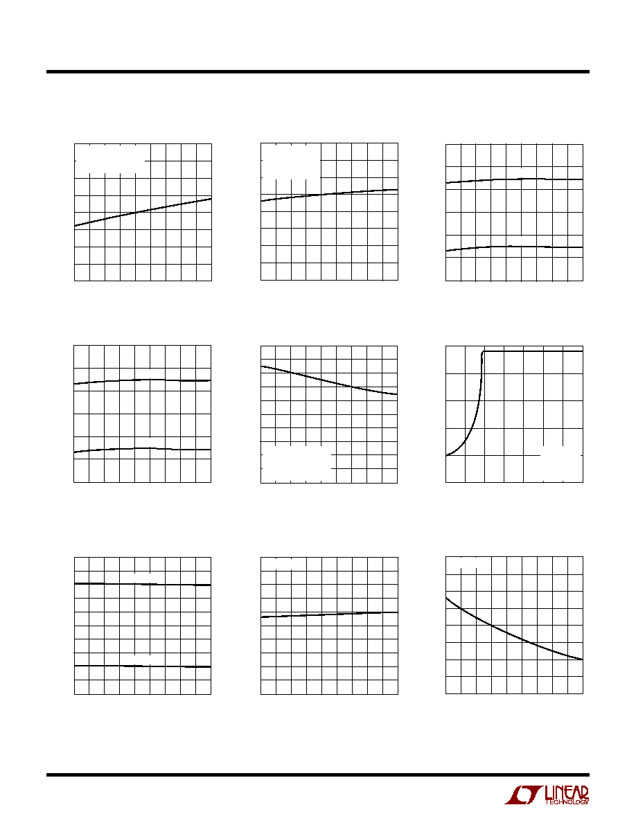
TYPICAL PERFOR A CE CHARACTERISTICS
U
W
I
GATE
(ACL, Sinking)
vs Temperature
I
GATE
(FCL, Sinking)
vs Temperature
V
GATE
vs Temperature
V
SS
vs Temperature
R
SS
vs Temperature
I
SS
(Sinking) vs Temperature
V
OS
vs Temperature
(V
ACL
+ V
OS
)/V
SS
vs Temperature
I
GATE
(Sourcing) vs Temperature
TEMPERATURE (
∞
C)
≠55 ≠35 ≠15
5
25
45
65
85 105 125
V
SS
(V)
4252-1/2 G26
2.40
2.35
2.30
2.25
2.20
2.15
2.10
2.05
2.00
TEMPERATURE (
∞
C)
≠55 ≠35 ≠15
5
25
45
65
85 105 125
R
SS
(k
)
4252-1/2 G28
110
108
106
104
102
100
98
96
94
92
90
TEMPERATURE (
∞
C)
≠55 ≠35 ≠15
0
I
SS
(mA)
5
15
20
25
65
85 105
45
4252-1/2 G39
10
5
25
45
125
30
35
40
UV = OV = V
SENSE
= V
EE
I
IN
= 2mA
V
SS
= 2V
TEMPERATURE (
∞
C)
≠55 ≠35 ≠15
5
25
45
65
85 105 125
V
OS
(mV)
4252-1/2 G29
11.0
10.8
10.6
10.4
10.2
10.0
9.8
9.6
9.4
9.2
9.0
TEMPERATURE (
∞
C)
≠55 ≠35 ≠15
5
25
45
65
85 105 125
(V
ACL
+ V
OS
)/V
SS
(V/V)
4252-1/2 G30
0.060
0.058
0.056
0.054
0.052
0.050
0.048
0.046
0.044
0.042
0.040
TEMPERATURE (
∞
C)
≠55
I
GATE
(
µ
A)
70
65
60
55
50
45
40
≠15
25
45
125
4252-1/2 G10
≠35
5
65
85 105
UV/0V = 4V
TIMER = 0V
V
SENSE
= V
EE
V
GATE
= 0V
TEMPERATURE (
∞
C)
≠55
I
GATE
(mA)
30
25
20
15
10
5
0
≠15
25
45
125
4252-1/2 G11
≠35
5
65
85 105
UV/0V = 4V
TIMER = 0V
V
SENSE
≠ V
EE
= 0.15V
V
GATE
= 3V
TEMPERATURE (
∞
C)
≠55
I
GATE
(mA)
400
350
300
250
200
150
100
50
0
≠15
25
45
125
4252-1/2 G12
≠35
5
65
85 105
UV/0V = 4V
TIMER = 0V
V
SENSE
≠ V
EE
= 0.3V
V
GATE
= 1V
TEMPERATURE (
∞
C)
≠55
V
GATE
(V)
14.5
14.0
13.5
13.0
12.5
12.0
11.5
11.0
10.5
10.0
≠15
25
45
125
4252-1/2 G13
≠35
5
65
85 105
UV/0V = 4V
TIMER = 0V
V
SENSE
= V
EE
LTC4252-1/LTC4252-2
6
425212f
TYPICAL PERFOR A CE CHARACTERISTICS
U
W
V
GATEH
vs Temperature
V
GATEL
vs Temperature
OV Threshold vs Temperature
I
SENSE
vs Temperature
UV Threshold vs Temperature
TIMER Threshold
vs Temperature
I
TMR
(Initial Cycle, Sourcing)
vs Temperature
TEMPERATURE (
∞
C)
≠55 ≠35 ≠15
5
25
45
65
85 105 125
V
GATEH
(V)
4252-1/2 G31
3.6
3.4
3.2
3.0
2.8
2.6
2.4
2.2
2.0
V
GATEH
= V
IN
≠ V
GATE
,
I
IN
= 2mA
(MS ONLY)
TEMPERATURE (
∞
C)
≠55
V
GATEL
(V)
0.8
0.7
0.6
0.5
0.4
0.3
0.2
0.1
0
≠15
25
45
125
4252-1/2 G14
≠35
5
65
85 105
UV/0V = 4V
TIMER = 0V
GATE THRESHOLD
BEFORE RAMP-UP
TEMPERATURE (
∞
C)
≠55
UV THRESHOLD (V)
3.375
3.275
3.175
3.075
2.975
2.875
2.775
≠15
25
45
125
4252-1/2 G15
≠35
5
65
85 105
V
UVH
V
UVL
I
SENSE
vs (V
SENSE
≠ V
EE
)
TEMPERATURE (
∞
C)
≠55
OV THRESHOLD (V)
6.45
6.25
6.05
5.85
5.65
5.45
5.25
≠15
25
45
125
4252-1/2 G16
≠35
5
65
85 105
V
OVH
V
OVL
TEMPERATURE (
∞
C)
≠55
I
SENSE
(
µ
A)
≠10
≠12
≠14
≠16
≠18
≠20
≠22
≠24
≠26
≠28
≠30
≠15
25
45
125
4252-1/2 G17
≠35
5
65
85 105
UV/0V = 4V
TIMER = 0V
GATE = HIGH
V
SENSE
≠ V
EE
= 50mV
(V
SENSE
≠ V
EE
) (V)
≠1.5
≠1.0 ≠0.5
0
0.5
1.0
1.5
2.0
≠I
SENSE
(mA)
0.01
0.1
1.0
10
100
1000
4252-1/2 G18
UV/0V = 4V
TIMER = 0V
GATE = HIGH
T
A
= 25
∞
C
TEMPERATURE (
∞
C)
≠55
TIMER THRESHOLD (V)
5.0
4.5
4.0
3.5
3.0
2.5
2.0
1.5
1.0
0.5
0
≠15
25
45
125
4252-1/2 G19
≠35
5
65
85 105
V
TMRH
V
TMRL
TEMPERATURE (
∞
C)
≠55
I
TMR
(
µ
A)
10
9
8
7
6
5
4
3
2
1
0
≠15
25
45
125
4252-1/2 G20
≠35
5
65
85 105
TIMER = 2V
I
TMR
(Initial Cycle, Sinking)
vs Temperature
TEMPERATURE (
∞
C)
≠55
I
TMR
(mA)
50
45
40
35
30
25
20
15
10
≠15
25
45
125
4252-1/2 G21
≠35
5
65
85 105
TIMER = 2V

LTC4252-1/LTC4252-2
7
425212f
TYPICAL PERFOR A CE CHARACTERISTICS
U
W
I
TMR
vs I
DRN
I
TMR
(Circuit Breaker, I
DRN
= 50
µ
A,
Sourcing) vs Temperature
I
DRN
vs V
DRAIN
V
DRNL
vs Temperature
V
DRNCL
vs Temperature
V
PGL
vs Temperature
I
TMR
(Circuit Breaker, Sourcing)
vs Temperature
I
TMR
(Cooling Cycle, Sinking)
vs Temperature
TEMPERATURE (
∞
C)
≠55
I
TMR
(
µ
A)
280
260
240
220
200
180
≠15
25
45
125
4252-1/2 G22
≠35
5
65
85 105
TIMER = 2V
I
DRN
= 0
µ
A
TEMPERATURE (
∞
C)
≠55 ≠35 ≠15
5
25
45
65
85 105 125
550
I
TMR
(
µ
A)
570
590
610
690
4252-1/2 G32
630
650
670
TIMER = 2V
I
DRN
= 50
µ
A
TEMPERATURE (
∞
C)
≠55
I
TMR
(
µ
A)
10
9
8
7
6
5
4
3
2
1
0
≠15
25
45
125
4252-1/2 G23
≠35
5
65
85 105
TIMER = 2V
I
DRN
(mA)
0.001
0.01
0.1
I
TMR
(mA)
1
10
0.1
1
10
4252-1/2 G33
I
TMRACC
/
I
DRN
vs Temperature
TEMPERATURE (
∞
C)
≠55 ≠35 ≠15
5
25
45
65
85 105 125
I
TMRACC
/
I
DRN
(
µ
A/
µ
A)
4252-1/2 G34
9.0
8.8
8.6
8.4
8.2
8.0
7.8
7.6
7.4
7.2
7.0
TIMER ON
(CIRCUIT BREAKING,
I
DRN
= 50
µ
A)
V
DRAIN
(V)
0
2
4
6
8
10
12
14
16
I
DRN
(mA)
100
10
1
0.1
0.01
0.001
0.0001
0.00001
4252-1/2
G25
I
IN
= 2mA
T
A
= ≠40
∞
C
T
A
= 25
∞
C
T
A
= 125
∞
C
T
A
= 85
∞
C
TEMPERATURE (
∞
C)
≠55 ≠35 ≠15
5
25
45
65
85 105 125
V
DRNL
(V)
4252-1/2 G35
2.60
2.55
2.50
2.45
2.40
2.35
2.30
2.25
2.20
FOR PWRGD STATUS (MS ONLY)
TEMPERATURE (
∞
C)
≠55 ≠35 ≠15
5
25
45
65
85 105 125
V
DRNCL
(V)
4252-1/2 G36
8.0
7.8
7.6
7.4
7.2
7.0
6.8
6.6
6.4
6.2
6.0
I
DRN
= 50
µ
A
TEMPERATURE (
∞
C)
≠55 ≠35 ≠15
5
25
45
65
85 105 125
V
PGL
(V)
4252-1/2 G37
3.0
2.5
2.0
1.5
1.0
0.5
0
(MS ONLY)
I
PG
= 10mA
I
PG
= 5mA
I
PG
= 1.6mA
LTC4252-1/LTC4252-2
8
425212f
TYPICAL PERFOR A CE CHARACTERISTICS
U
W
t
SS
vs Temperature
V
IN
(Pin 1/Pin 1): Positive Supply Input. Connect this pin
to the positive side of the supply through a dropping
resistor. A shunt regulator clamps V
IN
at 13V. An internal
undervoltage lockout (UVLO) circuit holds GATE low until
the V
IN
pin is greater than V
LKO
(9.2V), overriding UV and
OV. If UV is high, OV is low and V
IN
comes out of UVLO,
TIMER starts an initial timing cycle before initiating a GATE
ramp-up. If V
IN
drops below approximately 8.2V, GATE
pulls low immediately.
PWRGD (Pin 2/Not Available): Power Good Status Out-
put (MS only). At start-up, PWRGD latches low if DRAIN
is below 2.385V and GATE is within 2.8V of V
IN
. PWRGD
status is reset by UV, V
IN
(UVLO) or a circuit breaker fault
timeout. This pin is internally pulled high by a 58
µ
A current
source.
SS (Pin 3/Pin 2): Soft-Start Pin. This pin is used to ramp
inrush current during start up, thereby effecting control
over di/dt. A 20x attenuated version of the SS pin voltage
is presented to the current limit amplifier. This attenuated
voltage limits the MOSFET's drain current through the
sense resistor during the soft-start current limiting. At the
beginning of a start-up cycle, the SS capacitor (C
SS
) is
ramped by a 22
µ
A current source. The GATE pin is held
low until SS exceeds 20 ∑ V
OS
= 0.2V. SS is internally
shunted by a 100k resistor (R
SS
) which limits the SS pin
voltage to 2.2V. This corresponds to an analog current
limit SENSE voltage of 100mV. If the SS capacitor is
omitted, the SS pin ramps from 0V to 2.2V in about 220
µ
s.
The SS pin is pulled low under any of the following
conditions: in UVLO, in an undervoltage condition, in an
overvoltage condition, during the initial timing cycle or
when the circuit breaker fault times out.
SENSE (Pin 4/Pin 3): Circuit Breaker/Current Limit Sense
Pin. Load current is monitored by a sense resistor R
S
connected between
SENSE and V
EE
, and controlled in
three steps.
If SENSE exceeds V
CB
(50mV), the circuit
breaker comparator activates a (230
µ
A+8∑I
DRN
) TIMER
pull-up current. If SENSE exceeds V
ACL
(100mV), the
analog current limit amplifier pulls GATE down to regulate
the MOSFET current at V
ACL
/R
S
. In the event of a cata-
strophic short-circuit, SENSE may overshoot 100mV. If
SENSE reaches V
FCL
(200mV), the fast current limit com-
parator pulls GATE low with a strong pull-down. To disable
the circuit breaker and current limit functions, connect
SENSE
to V
EE
.
PI FU CTIO S
U
U
U
I
PGH
vs Temperature
t
PLLUG
and t
PHLOG
vs Temperature
TEMPERATURE
∞
(C)
≠55 ≠35 ≠15
5
25
45
65
85 105 125
I
PGH
(
µ
A)
4252-1/2 G38
62
61
60
59
58
57
56
55
V
PWRGD
= 0V
(MS ONLY)
TEMPERATURE (
∞
C)
≠55 ≠35 ≠15
5
25
45
65
85 105 125
t
SS
(
µ
s)
4252-1/2 G27
220
210
200
190
180
170
160
150
SS PIN FLOATING,
V
SS
RAMPS FROM 0.2V TO 2V
TEMPERATURE (
∞
C)
≠55
DELAY (
µ
s)
0.8
0.7
0.6
0.5
0.4
0.3
0.2
0.1
0
≠15
25
45
125
4252-1/2 G24
≠35
5
65
85 105
t
PLLUG
t
PHLOG
(MS/MS8)

LTC4252-1/LTC4252-2
9
425212f
V
EE
(Pin 5/Pin 4): Negative Supply Voltage Input. Connect
this pin to the negative side of the power supply.
GATE (Pin 6/Pin 5): N-Channel MOSFET Gate Drive Out-
put. This pin is pulled high by a 58
µ
A current source. GATE
is pulled low by invalid conditions at V
IN
(UVLO), UV, OV,
or a circuit breaker fault timeout. GATE is actively servoed
to control the fault current as measured at SENSE. A
compensation capacitor at GATE stabilizes this loop. A
comparator monitors GATE to ensure that it is low before
allowing an initial timing cycle, GATE ramp-up after an
overvoltage event or restart after a current limit fault.
During GATE start-up, a second comparator detects if
GATE is within 2.8V of V
IN
before PWRGD is set (MS
package only).
DRAIN (Pin7/Pin 6): Drain Sense Input. Connecting an
external resistor, R
D
,
between this pin and the MOSFET's
drain (V
OUT
) allows voltage sensing below 6.15V and
current feedback to TIMER. A comparator detects if DRAIN
is below 2.385V and together with the GATE high com-
parator sets the PWRGD flag. If V
OUT
is above V
DRNCL
,
DRAIN clamps at approximately V
DRNCL
. The current
through R
D
is internally multiplied by 8 and added to
TIMER's 230
µ
A pullup current during a circuit breaker
fault cycle. This reduces the fault time and MOSFET
heating.
OV (Pin 8/Pin7): Overvoltage Input. The active high thresh-
old at the OV pin is set at 6.15V with 0.6V hysteresis. If OV
> 6.15V, GATE pulls low. When OV returns below 5.55V,
GATE start-up begins without an initial timing cycle. If an
overvoltage condition occurs in the middle of an initial
timing cycle, the initial timing cycle is restarted after the
overvoltage condition goes away. An overvoltage condi-
tion does not reset the PWRGD flag. The internal UVLO at
V
IN
always overrides OV. A 1nF to 10nF capacitor at OV
prevents transients and switching noise from affecting the
OV thresholds and prevents glitches at the GATE pin.
UV (Pin 9/Pin 7): Undervoltage Input. The active low
threshold at the UV pin is set at 2.925V with 0.3V hyster-
esis. If UV < 2.925V, PWRGD pulls high, both GATE and
TIMER pull low. If UV rises above 3.225V, this initiates an
initial timing cycle followed by GATE start-up. The internal
UVLO at V
IN
always overrides UV. A low at UV resets an
internal fault latch. A 1nF to 10nF capacitor at UV prevents
transients and switching noise from affecting the UV
thresholds and prevents glitches at the GATE pin.
TIMER (Pin 10/Pin 8): Timer Input. TIMER is used to
generate an initial timing delay at start-up and to delay
shutdown in the event of an output overload (circuit
breaker fault). TIMER starts an initial timing cycle when
the following conditions are met: UV is high, OV is low, V
IN
clears UVLO, TIMER pin is low, GATE is lower than V
GATEL
,
SS < 0.2V, and V
SENSE
≠ V
EE
< V
CB
. A pull-up current of
5.8
µ
A then charges C
T
, generating a time delay. If C
T
charges to V
TMRH
(4V), the timing cycle terminates, TIMER
quickly pulls low and GATE is activated.
If SENSE exceeds 50mV while GATE is high, a circuit
breaker cycle begins with a 230
µ
A pull-up current charg-
ing C
T
. If DRAIN is approximately 7V during this cycle, the
timer pull-up has an additional current of 8 ∑ I
DRN
. If SENSE
drops below 50mV before TIMER reaches 4V, a 5.8
µ
A
pull-down current slowly discharges the C
T
. In the event
that C
T
eventually integrates up to the V
TMRH
threshold,
the circuit breaker trips, GATE quickly pulls low and
PWRGD pulls high. The LTC4252-1 TIMER pin latches
high with a 5.8
µ
A pull-up source. This latched fault is
cleared by either pulling TIMER low with an external device
or by pulling UV below 2.925V. The LTC4252-2 the starts
a shutdown cooling cycle following an overcurrent fault.
This cycle consists of 4 discharging ramps and 3 charging
ramps. The charging and discharging currents are 5.8
µ
A
and TIMER ramps between its 1V and 4V thresholds. At the
completion of a shutdown cooling cycle, the LTC4252-2
attempts a start-up cycle.
PI FU CTIO S
U
U
U
(MS/MS8)
LTC4252-1/LTC4252-2
10
425212f
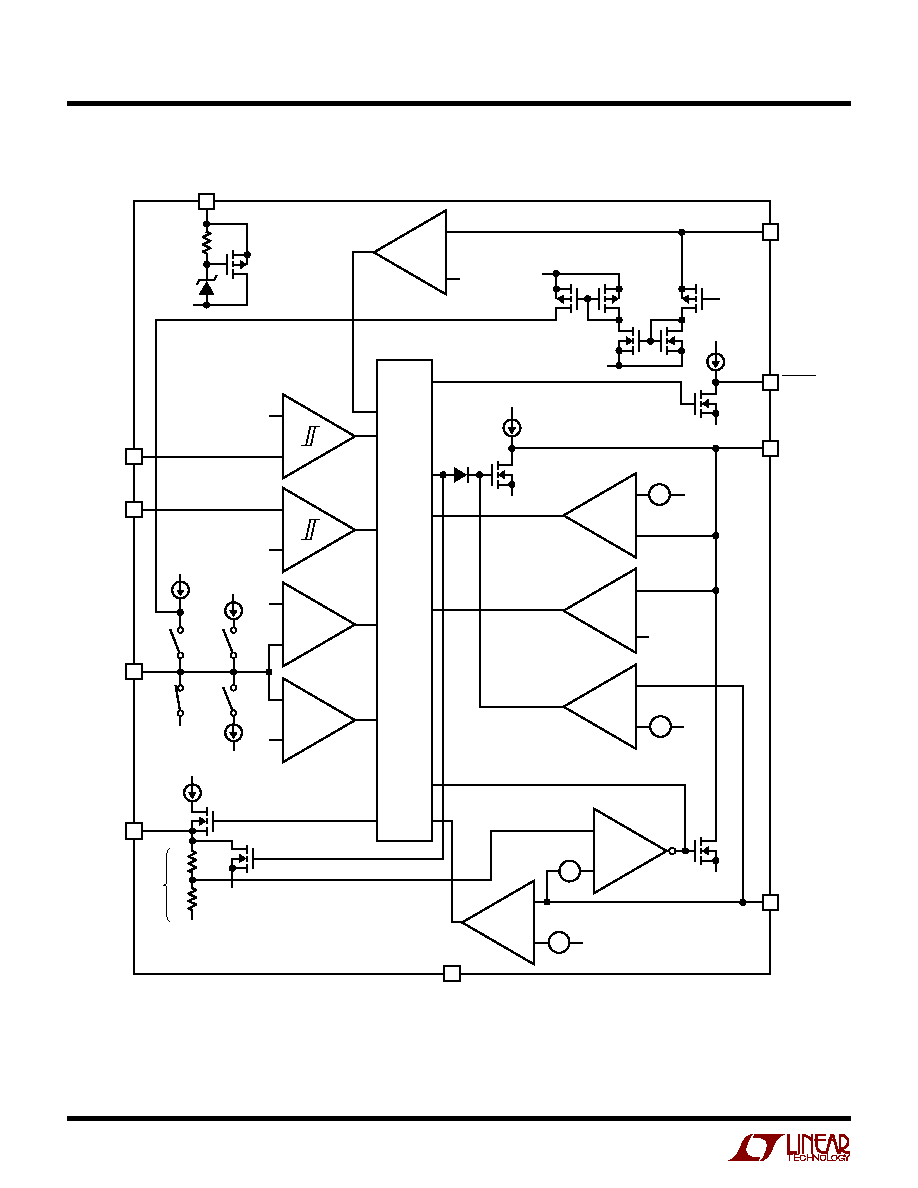
BLOCK DIAGRA
W
≠
+
4252-1/2 BD
≠
+
≠
+
≠
+
≠
+
+
≠
+
≠
V
IN
V
IN
V
EE
V
EE
R
SS
V
EE
V
EE
V
EE
0.5V
V
EE
V
EE
V
EE
5.8
µ
A
5.8
µ
A
V
IN
V
EE
V
IN
6.15V
58
µ
A
230
µ
A
V
IN
22
µ
A
95k
TIMER
6.15V
2.925V
4V
1V
+
≠
+
≠
2.385V
V
EE
V
EE
V
OS
= 10mV
V
IN
2.8V
≠
+
UV *
GATE
SENSE
V
IN
V
EE
58
µ
A
PWRGD **
DRAIN
OV *
SS
V
IN
CB
50mV
+
≠
≠
+
FCL
200mV
+
≠
ACL
5k
+
≠
1
◊
1
◊
8
◊
1
◊
LOGIC
*OV AND UV ARE TIED TOGETHER ON THE MS8 PACKAGE. OV AND UV ARE SEPARATE PINS ON THE MS PACKAGE
** ONLY AVAILABLE IN THE MS PACKAGE
LTC4252-1/LTC4252-2
11
425212f
4252-1/2 F01
LTC4252
C
LOAD
ISOLATED
DC/DC
CONVERTER
MODULE
LOW
VOLTAGE
CIRCUITRY
+
+
≠
≠
PLUG-IN BOARD
BACKPLANE
≠48RTN
≠48V
LONG
LONG
+
4252-1/2 F02
≠48RTN
≠48V
UV/OV
TIMER
V
EE
V
IN
SENSE
GATE
SS
DRAIN
LTC4252-1
R1
402k
1%
R2
32.4k
1%
R
D
1M
C
T
0.33
µ
F
C
SS
68nF
C
C
18nF
R
S
0.02
Q1
IRF530S
R
C
10
R
IN
10k
1/2W
1
7
8
2
6
5
3
4
C1
10nF
C
IN
1
µ
F
C
LOAD
100
µ
F
TYP
LONG
LONG
SHORT
+
Hot Circuit Insertion
When circuit boards are inserted into a live backplane, the
supply bypass capacitors can draw huge transient cur-
rents from the power bus as they charge. The flow of
current damages the connector pins and glitches the
power bus, causing other boards in the system to reset.
The LTC4252 is designed to turn on a circuit board supply
in a controlled manner, allowing insertion or removal
without glitches or connector damage.
Initial Start-Up
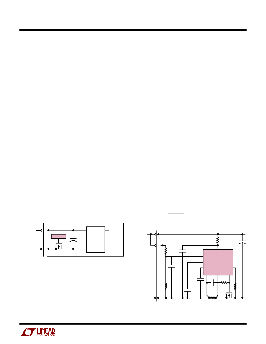
The LTC4252 resides on a removable circuit board and
controls the path between the connector and load or
power conversion circuitry with an external MOSFET switch
(see Figure 1). Both inrush control and short-circuit pro-
tection are provided by the MOSFET.
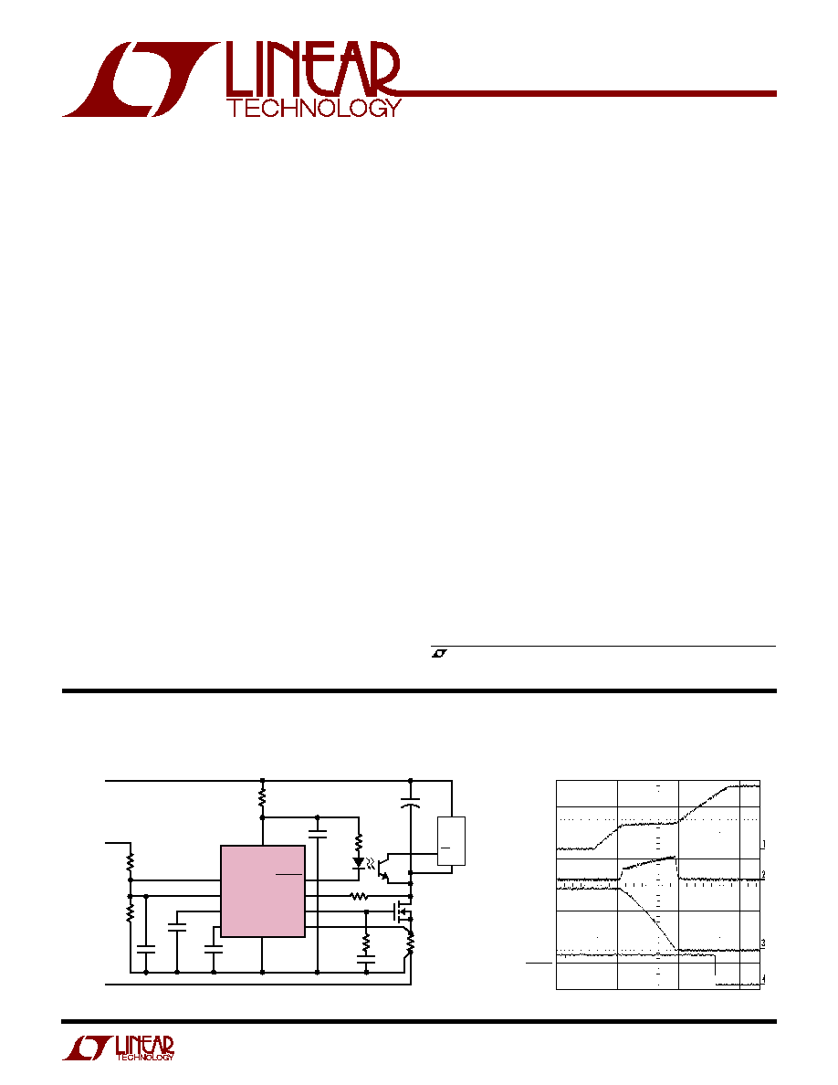
A detailed schematic is shown in Figure 2. ≠ 48V and
≠ 48RTN receive power through the longest connector
pins and are the first to connect when the board is inserted.
The GATE pin holds the MOSFET off during this time. UV/
OV determines whether or not the MOSFET should be
turned on based upon internal high accuracy thresholds
and an external divider. UV/OV does double duty by also
monitoring whether or not the connector is seated. The top
of the divider detects ≠ 48RTN by way of a short connector
pin that is the last to mate during the insertion sequence.
OPERATIO
U
Figure 1. Basic LTC4252 Hot Swap Topology
Figure 2. ≠48V, 2.5A Hot Swap Controller
Interlock Conditions
A start-up sequence commences once these "interlock"
conditions are met.
1. The input voltage V
IN
exceeds 9.2V (UVLO).
2. The voltage at UV > 3.225V.
3. The voltage at OV < 5.55V.
4. The (SENSE ≠ V
EE
) voltage is < 50mV (V
CB
).
5. The voltage at SS is < 0.2V (20 ∑ V
OS
).
6. The voltage on the TIMER capacitor (C
T
) is < 1V (V
TMRL
).
7. The voltage at GATE is < 0.5V (V
GATEL
).
The first three conditions are continuously monitored and
the latter four are checked prior to initial timing or GATE
ramp-up. Upon exiting an OV condition, the TIMER pin
voltage requirement is inhibited. Details are described in
the Applications Information, Timing Waveforms section.
TIMER begins the start-up sequence by sourcing 5.8
µ
A
into C
T
. If V
IN
, UV or OV falls out of range, the start-up cycle
stops and TIMER discharges C
T
to less than 1V, then waits
until the aforementioned conditions are once again met. If
C
T
successfully charges to 4V, TIMER pulls low and both
SS and GATE pins are released. GATE sources 58
µ
A
(I
GATE
), charging the MOSFET gate and associated capaci-
tance. The SS voltage ramp limits V
SENSE
to control the
inrush current. PWRGD pulls active low when GATE is
within 2.8V of V
IN
and DRAIN is lower than V
DRNL
.

LTC4252-1/LTC4252-2
12
425212f
OPERATIO
U
Two modes of operation are possible during the time the
MOSFET is first turning on, depending on the values of
external components, MOSFET characteristics and nomi-
nal design current. One possibility is that the MOSFET will
turn on gradually so that the inrush into the load capaci-
tance remains a low value. The output will simply ramp to
≠48V and the LTC4252 will fully enhance the MOSFET. A
second possibility is that the load current exceeds the soft-
start current limit threshold of [V
SS
(t)/20 ≠ V
OS
]/R
S
. In this
case the LTC4252 will ramp the output by sourcing soft-
start limited current into the load capacitance. If the soft-
start voltage is below 1.2V, the circuit breaker TIMER is
held low. Above 1.2V, TIMER ramps up. It is important to
set the timer delay so that, regardless of which start-up
mode is used, the TIMER ramp is less than one circuit
breaker delay time. If this condition is not met, the
LTC4252-1 may shut down after one circuit breaker delay
time whereas the LTC4252-2 may continue to autoretry.
Board Removal
If the board is withdrawn from the card cage, the UV/OV
divider is the first to lose connection. This shuts off the
MOSFET and commutates the flow of current in the
connector. When the power pins subsequently separate,
there is no arcing.
Current Control
Three levels of protection handle short-circuit and over-
load conditions. Load current is monitored by SENSE and
resistor R
S
. There are three distinct thresholds at SENSE:
50mV for a timed circuit breaker function; 100mV for an
analog current limit loop; and 200mV for a fast, feedforward
comparator which limits peak current in the event of a
catastrophic short-circuit.
If, owing to an output overload, the voltage drop across R
S
exceeds 50mV, TIMER sources 230
µ
A into C
T
. C
T
eventu-
ally charges to a 4V threshold and the LTC4252 shuts off.
If the overload goes away before C
T
reaches 4V and SENSE
measures less than 50mV, C
T
slowly discharges (5.8
µ
A).
In this way the LTC4252's circuit breaker function re-
sponds to low duty cycle overloads and accounts for fast
heating and slow cooling characteristics of the MOSFET.
Higher overloads are handled by an analog current limit
loop. If the drop across R
S
reaches 100mV, the current
limiting loop servos the MOSFET gate and maintains a
constant output current of 100mV/R
S
. In current limit
mode, V
OUT
typically rises and this increases MOSFET
heating. If V
OUT
> V
DRNCL
(7V), connecting an external
resistor, R
D
, between V
OUT
and DRAIN allows the fault
timing cycle to be shortened by accelerating the charging
of the TIMER capacitor. The TIMER pull-up current is
increased by 8 ∑ I
DRN
. Note that because SENSE > 50mV,
TIMER charges C
T
during this time and the LTC4252 will
eventually shut down.
Low impedance failures on the load side of the LTC4252
coupled with 48V or more driving potential can produce
current slew rates well in excess of 50A/
µ
s. Under these
conditions, overshoot is inevitable. A fast SENSE com-
parator with a threshold of 200mV detects overshoot and
pulls GATE low much harder and hence much faster than
the weaker current limit loop. The 100mV/R
S
current limit
loop then takes over and servos the current as previously
described. As before, TIMER runs and shuts down the
LTC4252 when C
T
reaches 4V.
If C
T
reaches 4V, the LTC4252-1 latches off with a 5.8
µ
A
pull-up current source whereas the LTC4252-2 starts a
shutdown cooling cycle. The LTC4252-1 circuit breaker
latch is reset by either pulling UV momentarily low or drop-
ping the input voltage V
IN
below the internal UVLO thresh-
old of 8.2V or pulling TIMER momentarily low with a switch.
The LTC4252-2 retries after its shutdown cooling cycle.
Although short-circuits are the most obvious fault type,
several operating conditions may invoke overcurrent pro-
tection. Noise spikes from the backplane or load, input
steps caused by the connection of a second, higher
voltage supply, transient currents caused by faults on
adjacent circuit boards sharing the same power bus or the
insertion of non-hot-swappable products could cause
higher than anticipated input current and temporary de-
tection of an overcurrent condition. The action of TIMER
and C
T
rejects these events allowing the LTC4252 to "ride
out" temporary overloads and disturbances that could trip
a simple current comparator and, in some cases, blow a
fuse.
LTC4252-1/LTC4252-2
13
425212f
APPLICATIO S I FOR ATIO
W
U
U
U
SHUNT REGULATOR
A fast responding regulator shunts the LTC4252 V
IN
pin.
Power is derived from ≠ 48RTN by an external current
limiting resistor. The shunt regulator clamps V
IN
to 13V
(V
Z
). A 1
µ
F decoupling capacitor at V
IN
filters supply
transients and contributes a short delay at start-up. R
IN
should be chosen to accommodate both V
IN
supply cur-
rent and the drive required for an optocoupler if the
PWRGD function on the 10-pin MS package is used.
Higher current through R
IN
results in higher dissipation
for R
IN
and the LTC4252. An alternative is a separate NPN
buffer driving the optocoupler as shown in Figure 3.
Multiple 1/4W resistors can replace a single higher power
R
IN
resistor.
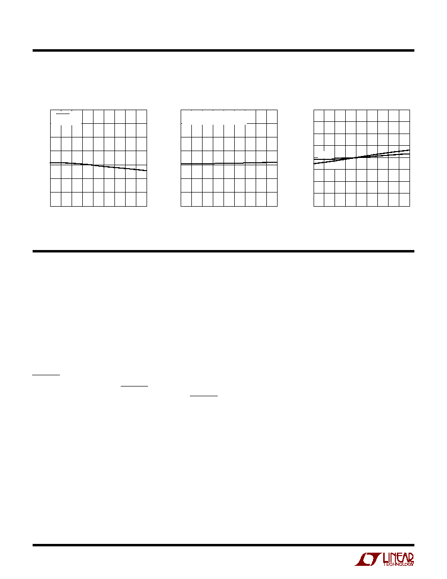
INTERNAL UNDERVOLTAGE LOCKOUT (UVLO)
A hysteretic comparator, UVLO, monitors V
IN
for
undervoltage. The thresholds are defined by V
LKO
and its
hysteresis, V
LKH
. When V
IN
rises above 9.2V (V
LKO
) the
chip is enabled; below 8.2V (V
LKO
≠ V
LKH
) it is disabled and
GATE is pulled low. The UVLO function at V
IN
should not
be confused with the UV/OV pin(s). These are completely
separate functions.
UV/OV COMPARATORS
An UV hysteretic comparator detects undervoltage condi-
tions at the UV pin, with the following thresholds:
UV low-to-high (V
UVHI
) = 3.225V
UV high-to-low (V
UVLO
) = 2.925V
An OV hysteretic comparator detects overvoltage condi-
tions at the OV pin, with the following thresholds:
OV low-to-high (V
OVHI
) = 6.150V
OV high-to-low (V
OVLO
) = 5.550V
The UV and OV trip point ratio is designed to match the
standard telecom operating range of 43V to 75V when
connected together as in Figure 2. A divider (R1, R2) is
used to scale the supply voltage. Using R1 = 402k and R2
= 32.4k gives a typical operating range of 43.2V to 74.4V.
The under- and overvoltage shutdown thresholds are then
39.2V and 82.5V. 1% divider resistors are recommended
to preserve threshold accuracy.
The R1-R2 divider values shown in the Typical Application
set a standing current of slightly more than 100
µ
A and
define an impedance at UV/OV of 30k
. In most applica-
tions, 30k
impedance coupled with 300mV UV hyster-
esis makes the LTC4252 insensitive to noise. If more noise
immunity is desired, add a 1nF to 10nF filter capacitor from
UV/OV to V
EE
.
Separate UV and OV pins are available in the 10-pin MS
package and can be used for a wider operating range such
as 35.5V to 76V as shown in Figure 3. Other combinations
are possible with different resistor arrangements.
4252-1/2 F03
GND
UV
OV
V
EE
V
IN
SENSE
SS
TIMER
GATE
PWRGD
DRAIN
LTC4252-1
R1
432k
1%
R3
32.4k
1%
R2
14k
1%
C
T
330nF
C
SS
68nF
C
C
18nF
≠48V
R
S
0.02
Q1
IRF530S
R
C
10
R5
2.2k
Q2
R
IN
10k
1/2W
1
9
8
10
3
2
7
6
4
5
C2
10nF
C
IN
1
µ
F
C
L
100
µ
F
GND
(SHORT PIN)
+
R
D
1M
LOAD
EN
R4
22k
*
* M0C207
Q2: MMBT5551LT1
Figure 3. ≠ 48V/2.5A Application with Wider Input Operating Range
LTC4252-1/LTC4252-2
14
425212f
UV/OV OPERATION
A low input to the UV comparator will reset the chip and
pull the GATE and TIMER pins low. A low-to-high UV
transition will initiate an initial timing sequence if the other
interlock conditions are met. A high-to-low transition in
the UV comparator immediately shuts down the LTC4252,
pulls the MOSFET gate low and resets the latched PWRGD
high.
Overvoltage conditions detected by the OV comparator
will also pull GATE low, thereby shutting down the load.
However, it will not reset the circuit breaker TIMER,
PWRGD flag or shutdown cooling timer. Returning the
supply voltage to an acceptable range restarts the GATE
pin if all the interlock conditions except TIMER are met.
Only during the initial timing cycle does an OV condition
reset the TIMER.
DRAIN
Connecting an external resistor, R
D
, to the dual function
DRAIN pin allows V
OUT
sensing without it being damaged
by large voltage transients. Below 6.15V, negligible pin
leakage allows a DRAIN low comparator to detect V
OUT
less than 2.385V (V
DRNL
). This condition, together with
the GATE low comparator, sets the PWRGD flag.
If V
OUT
> V
DRNCL
(7V), the DRAIN pin is clamped at about
7V and the current flowing in R
D
is given by:
I
V
V
R
DRN
OUT
DRNCL
D
-
(1)
This current is scaled up 8 times during a circuit breaker
fault and is added to the nominal 230
µ
A TIMER current.
This accelerates the fault TIMER pull-up when the MOSFET's
drain-source voltage exceeds 7V and effectively shortens
the MOSFET heating duration.
TIMER
The operation of the TIMER pin is somewhat complex as
it handles several key functions. A capacitor C
T
is used at
TIMER to provide timing for the LTC4252. Four different
charging and discharging modes are available at TIMER:
1) A 5.8
µ
A slow charge; initial timing and shutdown
cooling delay.
2) A (230
µ
A + 8 ∑ I
DRN
) fast charge; circuit breaker delay.
3) A 5.8
µ
A slow discharge; circuit breaker "cool off" and
shutdown cooling.
4) Low impedance switch; resets the TIMER capacitor
after an initial timing delay, in UVLO, in UV and in OV
during initial timing.
For initial start-up, the 5.8
µ
A pull-up is used. The low
impedance switch is turned off and the 5.8
µ
A current
source is enabled when the interlock conditions are met.
C
T
charges to 4V in a time period given by:
t
V C
A
T
=
µ
4
5 8
∑
.
(2)
When C
T
reaches 4V (V
TMRH
), the low impedance switch
turns on and discharges C
T
. A GATE start-up cycle begins
and both SS and GATE are released.
CIRCUIT BREAKER TIMER OPERATION
If the SENSE pin detects more than a 50mV drop across
R
S
, the TIMER pin charges C
T
with (230
µ
A + 8 ∑ I
DRN
). If
C
T
charges to 4V, the GATE pin pulls low and the LTC4252-1
latches off while the LTC4252-2 starts a shutdown cooling
cycle. The LTC4252-1 remains latched off until the UV pin
is momentarily pulsed low or TIMER is momentarily
discharged low by an external switch or V
IN
dips below
UVLO and is then restored. The circuit breaker timeout
period is given by:
t
V C
A
I
T
DRN
=
µ +
4
230
8
∑
∑
(3)
If V
OUT
< 6.15V, an internal PMOS device isolates any
DRAIN pin leakage current, making I
DRN
= 0
µ
A in Equation
(3). If V
OUT
> 7V (V
DRNCL
) during the circuit breaker fault
APPLICATIO S I FOR ATIO
W
U
U
U
LTC4252-1/LTC4252-2
15
425212f
period, the charging of C
T
accelerates by 8 ∑ I
DRN
of
Equation (1).
Intermittent overloads may exceed the 50mV threshold at
SENSE, but, if their duration is sufficiently short, TIMER
will not reach 4V and the LTC4252 will not shut the external
MOSFET off. To handle this situation, the TIMER dis-
charges C
T
slowly with a 5.8
µ
A pull-down whenever the
SENSE voltage is less than 50mV. Therefore, any intermit-
tent overload with V
OUT
< 6.15V and an aggregate duty
cycle of 2.5% or more will eventually trip the circuit
breaker and shut down the LTC4252. Figure 4 shows the
circuit breaker response time in seconds normalized to
1
µ
F for I
DRN
= 0
µ
A. The asymmetric charging and dis-
charging of C
T
is a fair gauge of MOSFET heating.
The normalized circuit response time is estimated by
t
C
F
I
D
T
DRN
(
)
.
∑
∑
.
µ
=
+
(
)
-
[
]
4
235 8 8
5 8
(4)
a shutdown cooling cycle begins if TIMER reaches the 4V
threshold. TIMER starts with a 5.8
µ
A pull-down until it
reaches the 1V threshold. Then, the 5.8
µ
A pull-up turns
back on until TIMER reaches the 4V threshold. Four 5.8
µ
A
pull-down cycles and three 5.8
µ
A pull-up cycles occur
between the 1V and 4V thresholds, creating a time interval
given by:
t
V C
A
SHUTDOWN
T
=
µ
7 3
5 8
∑
∑
.
(5)
At the 1V threshold of the last pull-down cycle, a GATE
ramp-up is attempted.
SOFT-START
Soft-start limits the inrush current profile during GATE
start-up. Unduly long soft-start intervals can exceed the
MOSFET's SOA rating if powering up into an active load. If
SS floats, an internal current source ramps SS from 0V to
2.2V in about 220
µ
s. Connecting an external capacitor C
SS
from SS to ground modifies the ramp to approximate an
RC response of:
V
t
V
e
SS
SS
t
R
C
SS
SS
( )
∑
∑
-
-
1
(6)
An internal resistor divider (95k/5k) scales V
SS
(t) down by
20 times to give the analog current limit threshold:
V
t
V
t
V
ACL
SS
OS
( )
( )
=
-
20
(7)
This allows the inrush current to be limited to V
ACL
(t)/R
S
.
The offset voltage, V
OS
(10mV), ensures C
SS
is sufficiently
discharged and the ACL amplifier is in current limit before
GATE start-up. SS is pulled low under any of the following
conditions: in UVLO, in an undervoltage condition, in an
overvoltage condition, during the initial timing cycle or
when the circuit breaker fault times out.
APPLICATIO S I FOR ATIO
W
U
U
U
FAULT DUTY CYCLE (%)
0
20
40
60
80
100
NORMALIZED RESPONSE TIME (s/
µ
F)
10
1
0.1
0.01
4252-1/2 F04
=
4
[(235.8 + 8 ∑ I
DRN
) ∑ D ≠ 5.8]
t
C
T
(
µ
F)
I
DRN
= 0
µ
A
Figure 4. Circuit-Breaker Response Time
SHUTDOWN COOLING CYCLE
For the LTC4252-1 (latchoff version), TIMER latches high
with a 5.8
µ
A pull-up after the circuit breaker fault TIMER
reaches 4V. For the LTC4252-2 (automatic retry version),
LTC4252-1/LTC4252-2
16
425212f
GATE
GATE is pulled low to V
EE
under any of the following
conditions: in UVLO, in an undervoltage condition, in an
overvoltage condition, during the initial timing cycle or
when the circuit breaker fault times out. When GATE turns
on, a 58
µ
A current source charges the MOSFET gate and
any associated external capacitance. V
IN
limits the gate
drive to no more than 14.5V.
Gate-drain capacitance (C
GD
) feedthrough at the first
abrupt application of power can cause a gate-source
voltage sufficient to turn on the MOSFET. A unique circuit
pulls GATE low with practically no usable voltage at V
IN
and eliminates current spikes at insertion. A large external
gate-source capacitor is thus unnecessary for the purpose
of compensating C
GD
. Instead, a smaller value (
10nF)
capacitor C
C
is adequate. C
C
also provides compensation
for the analog current limit loop.
GATE has two comparators: the GATE low comparator
looks for < 0.5V threshold prior to initial timing or a GATE
start-up cycle; the GATE high comparator looks for < 2.8V
relative to V
IN
and, together with the DRAIN low compara-
tor, sets PWRGD status during GATE startup.
SENSE
The SENSE pin is monitored by the circuit breaker (CB)
comparator, the analog current limit (ACL) amplifier and
the fast current limit (FCL) comparator. Each of these three
measures the potential of SENSE relative to V
EE
. When
SENSE exceeds 50mV, the CB comparator activates the
230
µ
A TIMER pull-up. At 100mV, the ACL amplifier servos
the MOSFET current and, at 200mV, the FCL comparator
abruptly pulls GATE low in an attempt to bring the MOSFET
current under control. If any of these conditions persists
long enough for TIMER to charge C
T
to 4V (see Equa-
tion 3), the LTC4252 shuts down and pulls GATE low.
If the SENSE pin encounters a voltage greater than 100mV,
the ACL amplifier will servo GATE downwards in an
attempt to control the MOSFET current. Since GATE over-
drives the MOSFET in normal operation, the ACL amplifier
needs time to discharge GATE to the threshold of the
MOSFET. For a mild overload the ACL amplifier can control
the MOSFET current, but in the event of a severe overload
the current may overshoot. At SENSE = 200mV the FCL
comparator takes over, quickly discharging the GATE pin
to near V
EE
potential. FCL then releases and the ACL
amplifier takes over. All the while TIMER is running. The
effect of FCL is to add a nonlinear response to the control
loop in favor of reducing MOSFET current.
Owing to inductive effects in the system, FCL typically
overcorrects the current limit loop and GATE under-
shoots. A zero in the loop (resistor R
C
in series with the
gate capacitor) helps the ACL amplifier to recover.
SHORT-CIRCUIT OPERATION
Circuit behavior arising from a load side low impedance
short is shown in Figure 5 for the LTC4252. Initially, the
current overshoots the fast current limit level of V
SENSE
=
200mV (Trace 2) as the GATE pin works to bring V
GS
under
control (Trace 3). The overshoot glitches the backplane in
the negative direction and when the current is reduced to
100mV/R
S
, the backplane responds by glitching in the
positive direction.
APPLICATIO S I FOR ATIO
W
U
U
U
4252-1/2 F05
≠48RTN
50V/DIV
GATE
10V/DIV
SENSE
200mV/DIV
TIMER
5V/DIV
0.5ms/DIV
FAST CURRENT LIMIT
SUPPLY RING OWING TO
CURRENT OVERSHOOT
SUPPLY RING OWING TO
MOSFET TURN OFF
ANALOG CURRENT LIMIT
ONSET OF OUTPUT SHORT-CIRCUIT
C
TIMER
RAMP
LATCH OFF
Figure 5. Output Short-Circuit Behavior of LTC4252

LTC4252-1/LTC4252-2
17
425212f
TIMER commences charging C
T
(Trace 4) while the analog
current limit loop maintains the fault current at 100mV/R
S
,
which in this case is 5A (Trace 2). Note that the backplane
voltage (Trace 1) sags under load. Timer pull-up is accel-
erated by V
OUT
. When C
T
reaches 4V, GATE turns off,
PWRGD pulls high, the load current drops to zero and the
backplane rings up to over 100V. The positive peak is
usually limited by avalanche breakdown in the MOSFET
and can be further limited by adding a zener diode across
the input from ≠ 48V to ≠ 48RTN, such as Diodes Inc.
SMAT70A.
A low impedance short on one card may influence the
behavior of others sharing the same backplane. The initial
glitch and backplane sag as seen in Figure 5 Trace 1, can
rob charge from output capacitors on adjacent cards.
When the faulty card shuts down, current flows in to
refresh the capacitors. If LTC4252s are used by the other
cards, they respond by limiting the inrush current to a
value of 100mV/R
S
. If C
T
is sized correctly, the capacitors
will recharge long before C
T
times out.
POWER GOOD, PWRGD
PWRGD latches low if GATE charges up to within 2.8V of
V
IN
and DRAIN pulls below V
DRNL
during start-up. PWRGD
is reset in UVLO, in a UV condition or if C
T
charges up to
4V. An overvoltage condition has no effect on PWRGD
status. A 58
µ
A current pulls this pin high during reset. Due
to voltage transients between the power module and
PWRGD, optoisolation is recommended. This pin pro-
vides sufficent drive for an optocoupler.
MOSFET SELECTION
The external MOSFET switch must have adequate safe
operating area (SOA) to handle short-circuit conditions
until TIMER times out. These considerations take prece-
dence over DC current ratings. A MOSFET with adequate
SOA for a given application can always handle the required
current, but the opposite may not be true. Consult the
manufacturer's MOSFET data sheet for safe operating area
and effective transient thermal impedance curves.
MOSFET selection is a 3-step process by assuming the
absense of a soft-start capacitor. First, R
S
is calculated and
then the time required to charge the load capacitance is
determined. This timing, along with the maximum short-
circuit current and maximum input voltage defines an
operating point that is checked against the MOSFET's SOA
curve.
To begin a design, first specify the required load current
and Ioad capacitance, I
L
and C
L
. The circuit breaker
current trip point (V
CB
/R
S
) should be set to accommodate
the maximum load current. Note that maximum input
current to a DC/DC converter is expected at V
SUPPLY(MIN)
.
R
S
is given by:
R
V
I
S
CB MIN
L MAX
=
(
)
(
)
(8)
where V
CB(MIN)
= 40mV represents the guaranteed mini-
mum circuit breaker threshold.
During the initial charging process, the LTC4252 may
operate the MOSFET in current limit, forcing (V
ACL
) be-
tween 80mV to 120mV across R
S
. The minimum inrush
current is given by:
I
mV
R
INRUSH MIN
S
(
)
=
80
(9)
Maximum short-circuit current limit is calculated using
the maximum V
SENSE
. This gives
I
mV
R
SHORTCIRCUIT MAX
S
(
)
=
120
(10)
The TIMER capacitor C
T
must be selected based on the
slowest expected charging rate; otherwise TIMER might
time out before the load capacitor is fully charged. A value
for C
T
is calculated based on the maximum time it takes the
load capacitor to charge. That time is given by:
t
C V
I
C
V
I
CL CHARGE
L
SUPPLY MAX
INRUSH MIN
(
)
(
)
(
)
∑
∑
=
=
(11)
APPLICATIO S I FOR ATIO
W
U
U
U
LTC4252-1/LTC4252-2
18
425212f
The maximum current flowing in the DRAIN pin is given
by:
I
V
V
R
DRN MAX
SUPPLY MAX
DRNCL
D
(
)
(
)
=
-
(12)
Approximating a linear charging rate as I
DRN
drops from
I
DRN(MAX)
to zero, the I
DRN
component in Equation (3) can
be approximated with 0.5 ∑ I
DRN(MAX)
. Rearranging equa-
tion, TIMER capacitor C
T
is given by:
C
t
A
I
V
T
CL CHARGE
DRN MAX
=
µ +
(
)
(
)
(
)
∑
∑
230
4
4
(13)
Returning to Equation (3), the TIMER period is calculated
and used in conjunction with V
SUPPLY(MAX)
and
I
SHORTCIRCUIT(MAX)
to check the SOA curves of a prospec-
tive MOSFET.
As a numerical design example, consider a 30W load,
which requires 1A input current at 36V. If V
SUPPLY(MAX)
=
72V and C
L
= 100
µ
F, R
D
= 1M
, Equation (8) gives R
S
=
40m
; Equation (13) gives C
T
= 441nF. To account for
errors in R
S
, C
T
, TIMER current (230
µ
A), TIMER threshold
(4V), R
D
, DRAIN current multiplier and DRAIN voltage
clamp (V
DRNCL
), the calculated value should be multiplied
by 1.5, giving the nearest standard value of C
T
= 680nF.
If a short-circuit occurs, a current of up to 120mV/
40m
= 3A will flow in the MOSFET for 3.6ms as dictated
by C
T
= 680nF in Equation (3). The MOSFET must be
selected based on this criterion. The IRF530S can handle
100V and 3A for 10ms and is safe to use in this application.
Computing the maximum soft-start capacitor value during
soft-start to a load short is complicated by the nonlinear
MOSFET's SOA characteristics and the R
SS
C
SS
response.
An overly conservative but simple approach begins with
the maximum circuit breaker current, given by:
I
mV
R
CB MAX
S
(
)
=
60
(14)
From the SOA curves of a prospective MOSFET, determine
the time allowed, t
SOA(MAX)
. C
SS
is given by:
C
t
R
SS
SOA MAX
SS
=
(
)
.
∑
0 916
(15)
In the above example, 60mV/40m
gives 1.5A. t
SOA(MAX)
for the IRF530S is 40ms. From Equation (15),
C
SS
= 437nF. Actual board evaluation showed that
C
SS
= 100nF was appropriate. The ratio (R
SS
∑ C
SS
) to
t
CL(CHARGE)
is a good gauge as a large ratio may result in
the time-out period expiring. This gauge is determined
empirically with board level evaluation.
SUMMARY OF DESIGN FLOW
To summarize the design flow, consider the application
shown in Figure 2. It was designed for 50W.
Calculate the maximum load current: 50W/36V = 1.4A;
allowing for 83% converter efficiency, I
IN(MAX)
= 1.7A.
Calculate R
S
: from Equation (8) R
S
= 20m
.
Calculate I
SHORTCIRCUIT(MAX)
: from Equation (9)
I
SHORTCIRCUIT(MAX)
= 6A.
Select a MOSFET that can handle 6A at 72V: IRF530S.
Calculate C
T
: from Equation (13) C
T
= 220nF. Select
C
T
= 330nF, which gives the circuit breaker time-out pe-
riod t
MAX
= 1.76ms.
Consult MOSFET SOA curves: the IRF530S can handle 6A
at 72V for 5ms, so it is safe to use in this application.
Calculate C
SS
: using Equations (14) and (15) select
C
SS
= 68nF.
FREQUENCY COMPENSATION
The LTC4252 typical frequency compensation network for
the analog current limit loop is a series R
C
(10
) and C
C
connected to V
EE
. Figure 6 depicts the relationship be-
tween the compensation capacitor C
C
and the MOSFET's
C
ISS
. The line in Figure 6 is used to select a starting value
APPLICATIO S I FOR ATIO
W
U
U
U

LTC4252-1/LTC4252-2
19
425212f
for C
C
based upon the MOSFET's C
ISS
specification. Opti-
mized values for C
C
are shown for several popular
MOSFETs. Differences in the optimized value of C
C
versus
the starting value are small. Nevertheless, compensation
values should be verified by board level short-circuit
testing.
As seen in Figure 5 previously, at the onset of a short-
circuit event, the input supply voltage can ring dramati-
cally owing to series inductance. If this voltage avalanches
the MOSFET, current continues to flow through the MOSFET
to the output. The analog current limit loop cannot control
this current flow and therefore the loop undershoots. This
effect cannot be eliminated by frequency compensation. A
zener diode is required to clamp the input supply voltage
and prevent MOSFET avalanche.
SENSE RESISTOR CONSIDERATIONS
For proper circuit breaker operation, Kelvin-sense PCB
connections between the sense resistor and the LTC4252's
V
EE
and SENSE pins are strongly recommended. The
drawing in Figure 7 illustrates the correct way of making
connections between the LTC4252 and the sense resistor.
PCB layout should be balanced and symmetrical to mini-
mize wiring errors. In addition, the PCB layout for the
sense resistor should include good thermal management
techniques for optimal sense resistor power dissipation.
TIMING WAVEFORMS
System Power-Up
Figure 8 details the timing waveforms for a typical power-
up sequence in the case where a board is already installed
in the backplane and system power is applied abruptly. At
time point 1, the supply ramps up, together with UV/OV,
V
OUT
and DRAIN. V
IN
and PWRGD follow at a slower rate
as set by the V
IN
bypass capacitor. At time point 2, V
IN
exceeds V
LKO
and the internal logic checks for UV > V
UVHI
,
OV < V
OVLO
, GATE < V
GATEL
, SENSE < V
CB
, SS < 20 ∑ V
OS
and TIMER < V
TMRL
. If all conditions are met, an initial
timing cycle starts and the TIMER capacitor is charged by
a 5.8
µ
A current source pull-up. At time point 3, TIMER
reaches the V
TMRH
threshold and the initial timing cycle
terminates. The TIMER capacitor is quickly discharged. At
time point 4, the V
TMRL
threshold is reached and the
conditions of GATE < V
GATEL
, SENSE < V
CB
and
SS < 20 ∑ V
OS
must be satisfied before a GATE ramp-up
cycle begins. SS ramps up as dictated by R
SS
∑ C
SS
(as in
Equation 6); GATE is held low by the analog current limit
(ACL) amplifier until SS crosses 20 ∑ V
OS
. Upon releasing
GATE, 58
µ
A sources into the external MOSFET gate and
compensation network. When the GATE voltage reaches
the MOSFET's threshold, current begins flowing into the
load capacitor at time point 5. At time point 6, load current
reaches the SS control level and the analog current limit
loop activates. Between time points 6 and 8, the GATE
voltage is servoed, the SENSE voltage is regulated at
APPLICATIO S I FOR ATIO
W
U
U
U
W
CURRENT FLOW
FROM LOAD
CURRENT FLOW
TO ≠48V BACKPLANE
SENSE RESISTOR
TRACK WIDTH W:
0.03" PER AMP
ON 1 OZ COPPER
TO
SENSE
TO
V
EE
4252-1/2 F07
Figure 7. Making PCB Connections to the Sense Resistor
MOSFET C
ISS
(pF)
0
COMPENSATION CAPACITANCE C
C
(nF)
60
50
40
30
20
10
0
2000
4000
4252-1/2 F06
6000
8000
NTY100N10
IRF3710
IRF540
IRF530
IRF740
Figure 6. Recommended Compensation
Capacitor C
C
vs MOSFET C
ISS
LTC4252-1/LTC4252-2
20
425212f
APPLICATIO S I FOR ATIO
W
U
U
U
GND ≠ V
EE
OR
(≠48RTN) ≠ (≠48V)
UV/OV
V
IN
TIMER
GATE
V
LKO
SENSE
V
IN
CLEARS V
LKO
, CHECK UV > V
UVHI
, OV < V
OVLO
, GATE < V
GATEL
, SENSE < V
CB
, SS < 20 ∑ V
OS
AND TIMER < V
TMRL
V
OUT
1
2
3 4 56
7
8
V
ACL
V
CB
9
TIMER CLEARS V
TMRL
, CHECK GATE < V
GATEL
, SENSE < V
CB
AND SS < 20 ∑ V
OS
SS
DRAIN
PWRGD
230
µ
A + 8 ∑ I
DRN
5.8
µ
A
20 ∑ V
OS
58
µ
A
10 11
V
IN
≠ V
GATEH
V
DRNL
V
DRNCL
20 ∑ (V
CB
+ V
OS
)
20 ∑ (V
ACL
+ V
OS
)
V
GATEL
V
TMRL
V
TMRH
5.8
µ
A
5.8
µ
A
58
µ
A
4252-1/2 F08
GATE
START-UP
INITIAL TIMING
Figure 8. System Power-Up Timing (All Waveforms are Referenced to V
EE
)
V
ACL
(t) (Equation 7) and soft-start limits the slew rate of
the load current. If the SENSE voltage (V
SENSE
≠ V
EE
)
reaches the V
CB
threshold at time point 7, the circuit
breaker TIMER activates. The TIMER capacitor, C
T
, is
charged by a (230
µ
A + 8 ∑ I
DRN
) current pull-up. As the load
capacitor nears full charge, load current begins to decline.
At time point 8, the load current falls and the SENSE
voltage drops below V
ACL
(t). The analog current limit loop
shuts off and the GATE pin ramps further. At time point 9,
the SENSE voltage drops below V
CB
, the fault TIMER cycle
ends, followed by a 5.8
µ
A discharge cycle (cool off). The
duration between time points 7 and 9 must be shorter than
one circuit breaker delay to avoid a fault time out during
GATE ramp-up. When GATE ramps past the V
GATEH
thresh-
old at time point 10, PWRGD pulls low. At time point 11,
GATE reaches its maximum voltage as determined by V
IN
.
Live Insertion with Short Pin Control of UV/OV
In the example shown in Figure 9, power is delivered
through long connector pins whereas the UV/OV divider
makes contact through a short pin. This ensures the power
connections are firmly established before the LTC4252 is
activated. At time point 1, the power pins make contact and
LTC4252-1/LTC4252-2
21
425212f
APPLICATIO S I FOR ATIO
W
U
U
U
Figure 9. Power-Up Timing with a Short Pin (All Waveforms are Referenced to V
EE
)
5.8
µ
A
58
µ
A
5.8
µ
A
5.8
µ
A
58
µ
A
GATE
START-UP
INITIAL TIMING
UV CLEARS V
UVHI
, CHECK OV < V
OVHI
, GATE < V
GATEL
, SENSE < V
CB
, SS < 20 ∑ V
OS
AND TIMER < V
TMRL
1
2
3 4 56
7
8 9
TIMER CLEARS V
TMRL
, CHECK GATE < V
GATEL
, SENSE < V
CB
AND SS < 20 ∑ V
OS
1011
4252-1/2 F09
GND ≠ V
EE
OR
(≠48RTN) ≠ (≠48V)
UV/OV
V
IN
TIMER
GATE
SENSE
V
OUT
SS
DRAIN
PWRGD
V
LKO
V
UVHI
V
ACL
V
CB
230
µ
A + 8 ∑ I
DRN
20 ∑ V
OS
V
IN
≠ V
GATEH
V
DRNL
V
DRNCL
20 ∑ (V
CB
+ V
OS
)
20 ∑ (V
ACL
+ V
OS
)
V
GATEL
V
TMRL
V
TMRH
V
IN
ramps through V
LKO
. At time point 2, the UV/OV divider
makes contact and its voltage exceeds V
UVHI
. In addition,
the internal logic checks for OV < V
OVHI
, GATE < V
GATEL
,
SENSE < V
CB
, SS < 20 ∑ V
OS
and TIMER < V
TMRL
. If all
conditions are met, an initial timing cycle starts and the
TIMER capacitor is charged by a 5.8
µ
A current source
pull-up. At time point 3, TIMER reaches the V
TMRH
thresh-
old and the initial timing cycle terminates. The TIMER
capacitor is quickly discharged. At time point 4, the V
TMRL
threshold is reached and the conditions of GATE < V
GATEL
,
SENSE < V
CB
and SS < 20 ∑ V
OS
must be satisfied before
a GATE start-up cycle begins. SS ramps up as dictated by
R
SS
∑ C
SS
; GATE is held low by the analog current limit
amplifier until SS crosses 20 ∑ V
OS
. Upon releasing GATE,
58
µ
A sources into the external MOSFET gate and compen-
sation network. When the GATE voltage reaches the
MOSFET's threshold, current begins flowing into the load
capacitor at time point 5. At time point 6, load current
reaches the SS control level and the analog current limit
loop activates. Between time points 6 and 8, the GATE
voltage is servoed, the SENSE voltage is regulated at
V
ACL
(t) and soft-start limits the slew rate of the load
current. If the SENSE voltage (V
SENSE
≠ V
EE
) reaches the
V
CB
threshold at time point 7, the circuit breaker TIMER
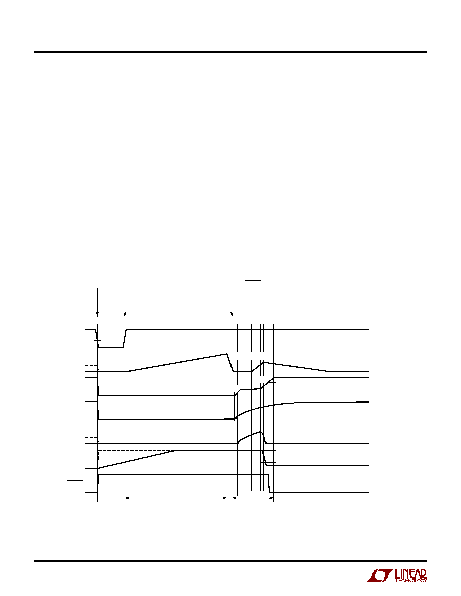
LTC4252-1/LTC4252-2
22
425212f
Figure 10. Undervoltage Timing (All Waveforms are Referenced to V
EE
)
UV
TIMER
GATE
SENSE
SS
DRAIN
PWRGD
5.8
µ
A
58
µ
A
5.8
µ
A
5.8
µ
A
58
µ
A
UV DROPS BELOW V
UVLO
. GATE, SS AND TIMER ARE PULLED DOWN, PWRGD RELEASES
1
2
3 4 56
7
8 9
TIMER CLEARS V
TMRL
, CHECK GATE < V
GATEL
, SENSE < V
CB
AND SS < 20 ∑ V
OS
10 11
4252-1/2 F10
UV CLEARS V
UVHI
, CHECK OV CONDITION, GATE < V
GATEL
, SENSE < V
CB
, SS < 20 ∑ V
OS
AND TIMER < V
TMRL
V
ACL
V
CB
230
µ
A + 8 ∑ I
DRN
20 ∑ V
OS
V
IN
≠ V
GATEH
V
DRNL
V
DRNCL
20 ∑ (V
CB
+ V
OS
)
20 ∑ (V
ACL
+ V
OS
)
V
GATEL
V
TMRL
V
TMRH
V
UVHI
V
UVLO
GATE
START-UP
INITIAL TIMING
APPLICATIO S I FOR ATIO
W
U
U
U
activates. The TIMER capacitor, C
T
, is charged by a (230
µ
A
+ 8 ∑ I
DRN
) current pull-up. As the load capacitor nears full
charge, load current begins to decline. At point 8, the load
current falls and the SENSE voltage drops below V
ACL
(t).
The analog current limit loop shuts off and the GATE pin
ramps further. At time point 9, the SENSE voltage drops
below V
CB
and the fault TIMER cycle ends, followed by a
5.8
µ
A discharge cycle (cool off). When GATE ramps past
V
GATEH
threshold at time point 10, PWRGD pulls low. At
time point 11, GATE reaches its maximum voltage as
determined by V
IN
.
Undervoltage Timing
In Figure 10 when UV pin drops below V
UVLO
(time
point 1), the LTC4252 shuts down with TIMER, SS and
GATE all pulling low. If current has been flowing, the
SENSE pin voltage decreases to zero as GATE collapses.
When UV recovers and clears V
UVHI
(time point 2), an
initial timer cycle begins followed by a start-up cycle.
V
IN
Undervoltage Lockout Timing
The V
IN
undervoltage lockout comparator, UVLO, has a
similar timing behavior as the UV pin timing except it looks
for V
IN
< (V
LKO
≠ V
LKH
) to shut down and V
IN
> V
LKO
to
start. In an undervoltage lockout condition, both UV and
OV comparators are held off. When V
IN
exits undervoltage
lockout, the UV and OV comparators are enabled.
Undervoltage Timing with Overvoltage Glitch
In Figure 11, both UV and OV pins are connected together.
When UV clears V
UVHI
(time point 1), an initial timing cycle
starts. If the system bus voltage overshoots V
OVHI
as
shown at time point 2, TIMER discharges. At time point 3,
the supply voltage recovers and drops below the V
OVLO
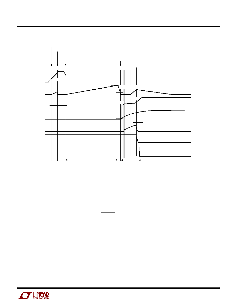
LTC4252-1/LTC4252-2
23
425212f
APPLICATIO S I FOR ATIO
W
U
U
U
Figure 11. Undervoltage Timing with an Overvoltage Glitch (All Waveforms are Referenced to V
EE
)
UV/OV
TIMER
GATE
SENSE
SS
DRAIN
PWRGD
5.8
µ
A
58
µ
A
58
µ
A
5.8
µ
A
5.8
µ
A
UV/OV CLEARS V
UVHI
, CHECK OV CONDITION, GATE < V
GATEL
, SENSE < V
CB
, SS < 20 ∑ V
OS
AND TIMER < V
TMRL
1
2
3
4 5 67
8
9
TIMER CLEARS V
TMRL
, CHECK GATE < V
GATEL
, SENSE < V
CB
AND SS < 20 ∑ V
OS
10
11
12
4252-1/2 F11
UV/OV DROPS BELOW V
OVLO
AND TIMER RESTARTS INITIAL TIMING CYCLE
UV/OV OVERSHOOTS V
OVHI
AND TIMER ABORTS INITIAL TIMING CYCLE
V
ACL
V
CB
230
µ
A + 8 ∑ I
DRN
20 ∑ V
OS
V
IN
≠ V
GATEH
V
DRNL
V
DRNCL
20 ∑ (V
CB
+ V
OS
)
20 ∑ (V
ACL
+ V
OS
)
V
GATEL
V
TMRL
V
TMRH
V
OVHI
V
UVHI
V
OVLO
GATE
START-UP
INITIAL TIMING
threshold. The initial timing cycle restarts, followed by a
GATE start-up cycle.
Overvoltage Timing
During normal operation, if the OV pin exceeds V
OVHI
as
shown at time point 1 of Figure 12, the TIMER and PWRGD
status are unaffected. Nevertheless, SS and GATE pull
down and the load is disconnected. At time point 2, OV
recovers and drops below the V
OVLO
threshold. A GATE
start-up cycle begins. If the overvoltage glitch is long
enough to deplete the load capacitor, a full start-up cycle
as shown between time points 4 through 7 may occur.
Circuit Breaker Timing
In Figure 13a, the TIMER capacitor charges at 230
µ
A if the
SENSE pin exceeds V
CB
but V
DRN
is less than 6.15V. If the
SENSE pin drops below V
CB
before TIMER reaches the
V
TMRH
threshold, TIMER is discharged by 5.8
µ
A. In Figure
13b, when TIMER exceeds V
TMRH
, GATE pulls down
immediately and the LTC4252 shuts down. In Figure 13c,
multiple momentary faults cause the TIMER capacitor to
integrate and reach V
TMRH
. GATE pull down follows and
the LTC4252 shuts down. During shutdown, the LTC4252-1
latches TIMER high with a 5.8
µ
A pull-up current source;
the LTC4252-2 activates a shutdown cooling cycle.
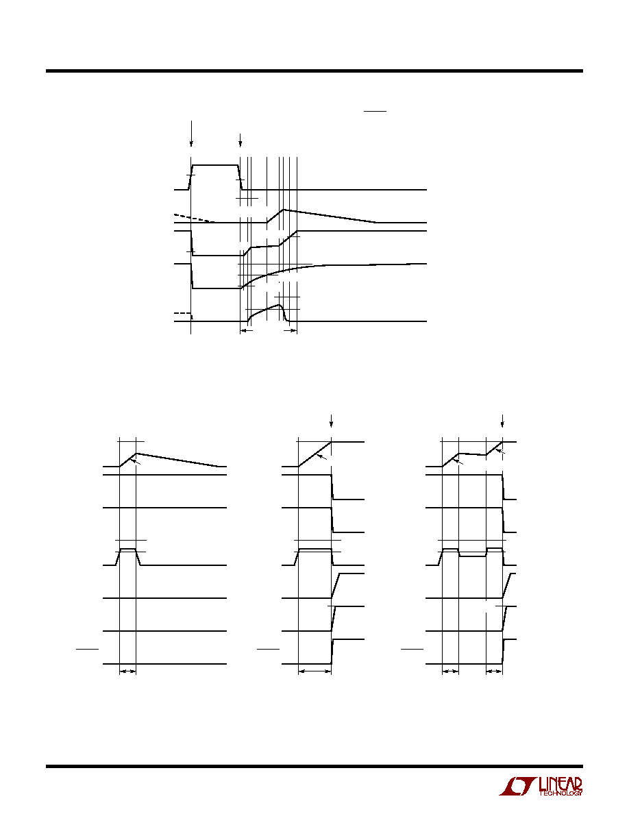
LTC4252-1/LTC4252-2
24
425212f
APPLICATIO S I FOR ATIO
W
U
U
U
(13a) Momentary Circuit-Breaker Fault
Figure 13. Circuit-Breaker Timing Behavior (All Waveforms are Referenced to V
EE
)
(13b) Circuit-Breaker Time Out
(13c) Multiple Circuit-Breaker Fault
CB FAULT
TIMER
GATE
SENSE
V
OUT
SS
DRAIN
PWRGD
TIMER
GATE
SENSE
V
OUT
SS
DRAIN
PWRGD
TIMER
GATE
SENSE
V
OUT
SS
DRAIN
PWRGD
CB FAULT
CB FAULT
CB FAULT
5.8
µ
A
5.8
µ
A
1
2
4252-1/2 F13
1
2
CB TIMES OUT
1
4
3
2
CB TIMES OUT
V
ACL
V
CB
V
ACL
V
DRNCL
V
CB
V
ACL
V
TMRH
V
TMRH
V
TMRH
V
CB
230
µ
A + 8 ∑ I
DRN
V
DRNCL
230
µ
A + 8 ∑ I
DRN
230
µ
A + 8 ∑ I
DRN
230
µ
A + 8 ∑ I
DRN
Figure 12. Overvoltage Timing (All Waveforms are Referenced to V
EE
)
OV
TIMER
GATE
SENSE
SS
5.8
µ
A
58
µ
A
58
µ
A
5.8
µ
A
1
2 34
5
67 8 9
4252-1/2 F12
OV DROPS BELOW V
OVLO
, CHECK GATE < V
GATEL
, SENSE < V
CB
AND SS < 20 ∑ V
OS
OV OVERSHOOTS V
OVHI
. GATE AND SS ARE PULLED DOWN, PWRGD AND TIMER ARE UNAFFECTED
V
ACL
V
CB
230
µ
A + 8 ∑ I
DRN
20 ∑ V
OS
V
IN
≠ V
GATEH
20 ∑ (V
CB
+ V
OS
)
20 ∑ (V
ACL
+ V
OS
)
V
GATEL
V
OVHI
V
TMRH
V
OVLO
GATE
START-UP
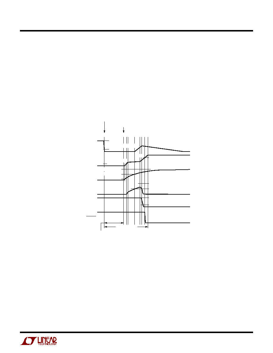
LTC4252-1/LTC4252-2
25
425212f
APPLICATIO S I FOR ATIO
W
U
U
U
Resetting a Fault Latch (LTC4252-1)
The latched circuit breaker fault of LTC4252-1 benefits
from long cooling time. It is reset by pulling the UV pin
below V
UVLO
with a switch. Reset is also accomplished by
pulling the V
IN
pin momentarily below (V
LKO
≠ V
LKH
). A
third reset method involves pulling the TIMER pin below
V
TMRL
as shown in Figure 14. An initial timing cycle is
skipped if TIMER is used for reset. An initial timing cycle
is generated if reset by the UV pin or the V
IN
pin.
Figure 14. Pushbutton Reset of LTC4252-1's Latched Fault (All Waveforms are Referenced to V
EE
)
TIMER
GATE
SENSE
V
ACL
V
CB
SS
DRAIN
230
µ
A + 8 ∑ I
DRN
V
IN
≠ V
GATEH
V
DRNL
4252-1/2 F14
V
DRNCL
V
GATEL
V
TMRL
V
TMRH
PWRGD
5.8
µ
A
5.8
µ
A
5.8
µ
A
58
µ
A
58
µ
A
1
2 34
5
67 8 9
SWITCH RELEASES SS
SWITCH RESETS LATCHED TIMER
GATE START-UP
20 ∑ V
OS
20 ∑ (V
CB
+ V
OS
)
20 ∑ (V
ACL
+ V
OS
)
MOMENTARY DPST SWITCH RESET
The duration of the TIMER reset pulse should be smaller
than the time taken to reach 0.2V at SS pin. With a single
pole mechanical pushbutton switch, this may not be
feasible. A double pole, single throw pushbutton switch
removes this restriction by connecting the second switch
to the SS pin. With this method, both the SS and TIMER
pins are released at the same time (see Figure 19).
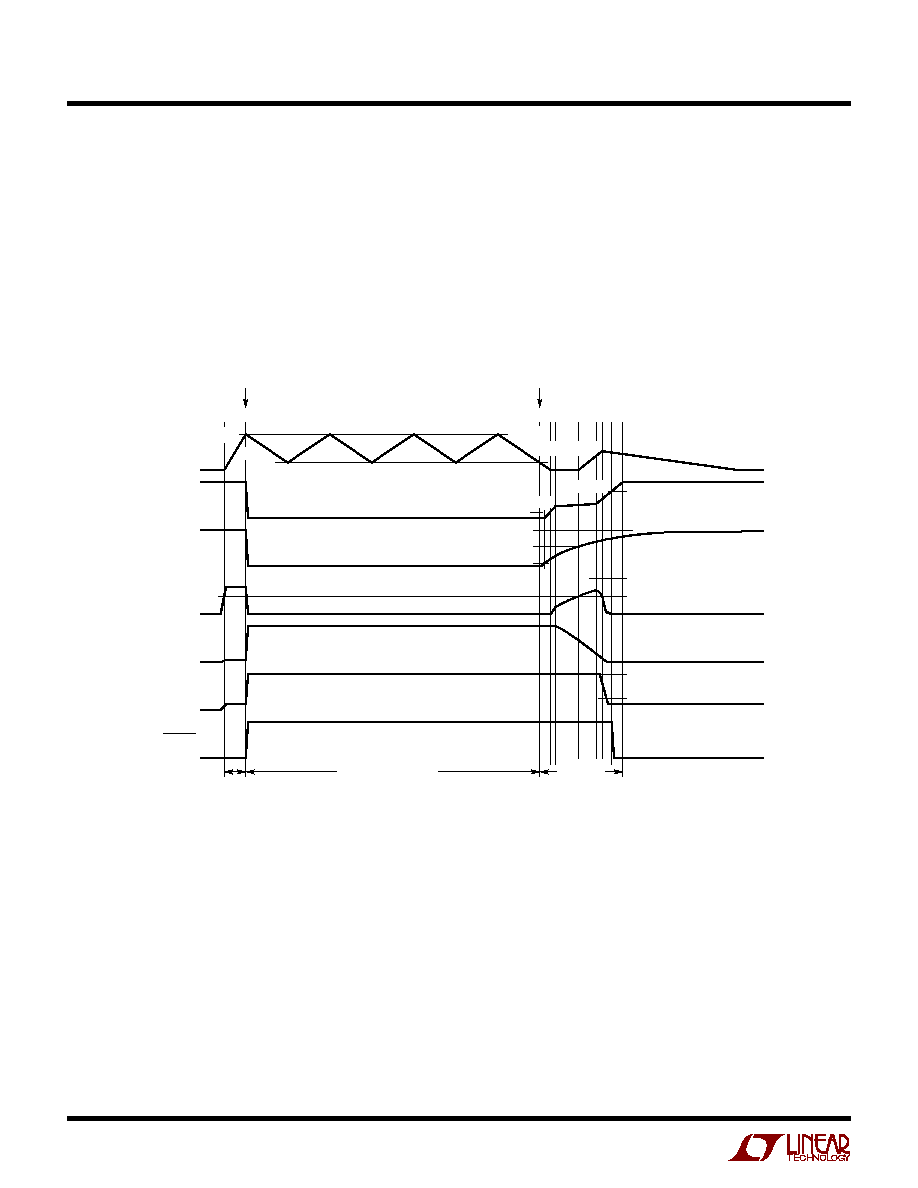
LTC4252-1/LTC4252-2
26
425212f
APPLICATIO S I FOR ATIO
W
U
U
U
Shutdown Cooling Cycle (LTC4252-2)
Figure 15 shows the timer behavior of the LTC4252-2. At
time point 2, TIMER exceeds V
TMRH
, GATE pulls down
immediately and the LTC4252 shuts down. TIMER starts
a shutdown cooling cycle by discharging TIMER with
5.8
µ
A to the V
TMRL
threshold. TIMER then charges with
5.8
µ
A to the V
TMRH
threshold. There are four 5.8
µ
A
Figure 15. Shutdown Cooling Timing Behavior of LTC4252-2 (All Waveforms are Referenced to V
EE
)
TIMER
GATE
SENSE
V
OUT
V
ACL
V
CB
SS
DRAIN
230
µ
A + 8 ∑ I
DRN
V
TMRH
V
TMRL
V
GATEL
230
µ
A + 8 ∑ I
DRN
V
IN
≠ V
GATEH
V
DRNL
4252-1/2 F15
V
DRNCL
PWRGD
58
µ
A
58
µ
A
5.8
µ
A
5.8
µ
A
5.8
µ
A
5.8
µ
A
5.8
µ
A
5.8
µ
A
5.8
µ
A
5.8
µ
A
5.8
µ
A
GATE
START-UP
SHUTDOWN COOLING
CB
20 ∑ V
OS
20 ∑ (V
CB
+ V
OS
)
20 ∑ (V
ACL
+ V
OS
)
1
2
3 4 5
6
78 9 10
RETRY
CIRCUIT BREAKER TIMES OUT
discharge phases and three 5.8
µ
A charge phases in this
shutdown cooling cycle spanning time points 2 and 3. At
time point 3, the LTC4252 automatic retry occurs with a
start-up cycle. Good thermal management techniques are
highly recommended; power and thermal dissipation must
be carefully evaluated when implementing the automatic
retry scheme.
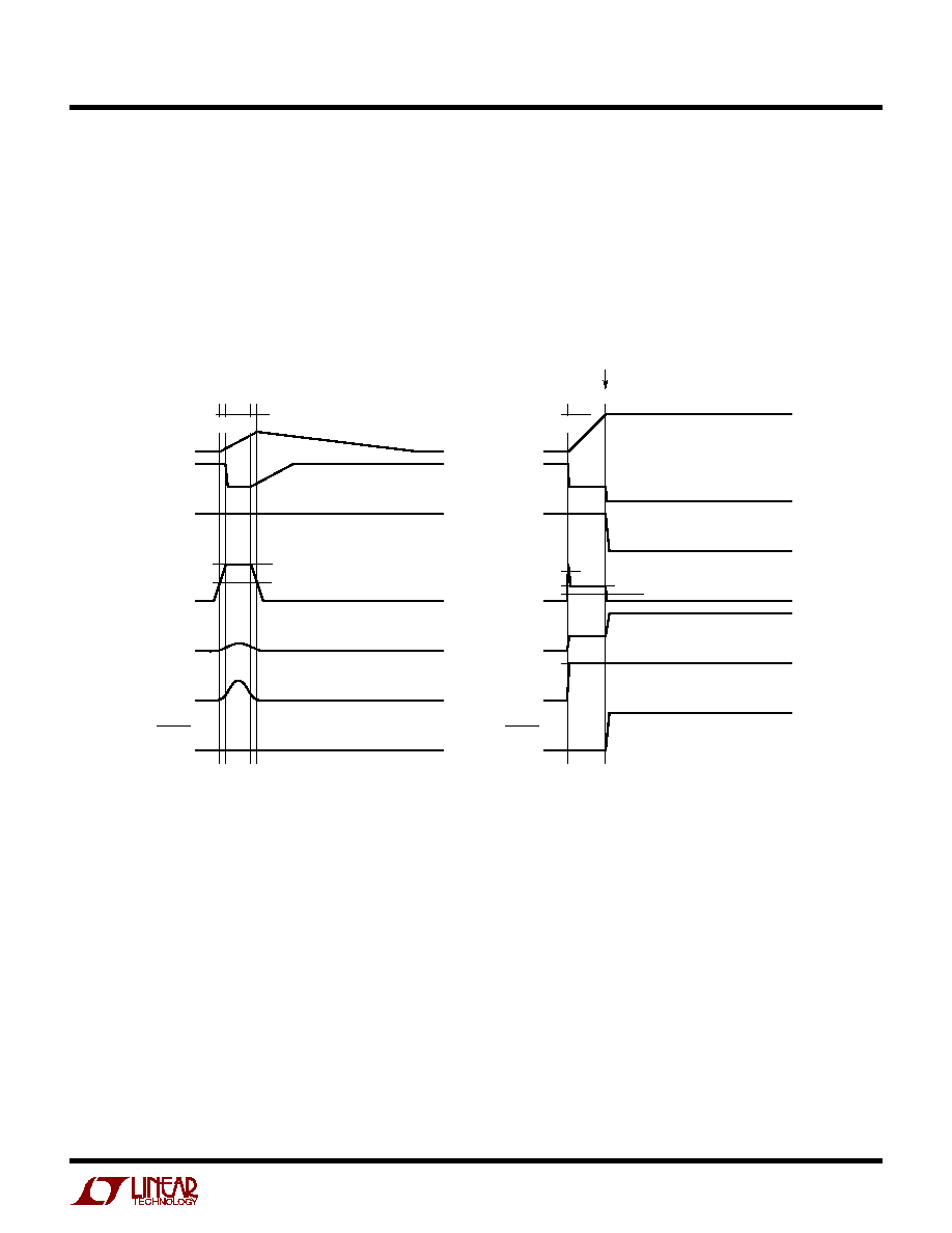
LTC4252-1/LTC4252-2
27
425212f
APPLICATIO S I FOR ATIO
W
U
U
U
Figure 16. Current Limit Behavior (All Waveforms are Referenced to V
EE
)
(16a) Analog Current Limit Fault
(16b) Fast Current Limit Fault
TIMER
GATE
SENSE
V
OUT
V
ACL
V
CB
SS
DRAIN
V
TMRH
230
µ
A + 8 ∑ I
DRN
4252-1/2 F16
PWRGD
5.8
µ
A
5.8
µ
A
TIMER
GATE
SENSE
V
OUT
V
ACL
V
CB
V
FCL
SS
DRAIN
V
TMRH
V
DRNCL
230
µ
A + 8 ∑ I
DRN
PWRGD
1
2
1
4
3
2
CB TIMES OUT
Analog Current Limit and Fast Current Limit
In Figure 16a, when SENSE exceeds V
ACL
, GATE is regu-
lated by the analog current limit amplifier loop. When
SENSE drops below V
ACL
, GATE is allowed to pull up. In
Figure 16b, when a severe fault occurs, SENSE exceeds
V
FCL
and GATE immediately pulls down until the analog
current amplifier can establish control. If the severe fault
causes V
OUT
to exceed V
DRNCL
, the DRAIN pin is clamped
at V
DRNCL
. I
DRN
flows into the DRAIN pin and is multiplied
by 8. This extra current is added to the TIMER pull-up
current of 230
µ
A. This accelerated TIMER current of
[230
µ
A+8 ∑ I
DRN
] produces a shorter circuit breaker fault
delay. Careful selection of C
T
, R
D
and MOSFET can help
prevent SOA damage in a low impedance fault condition.
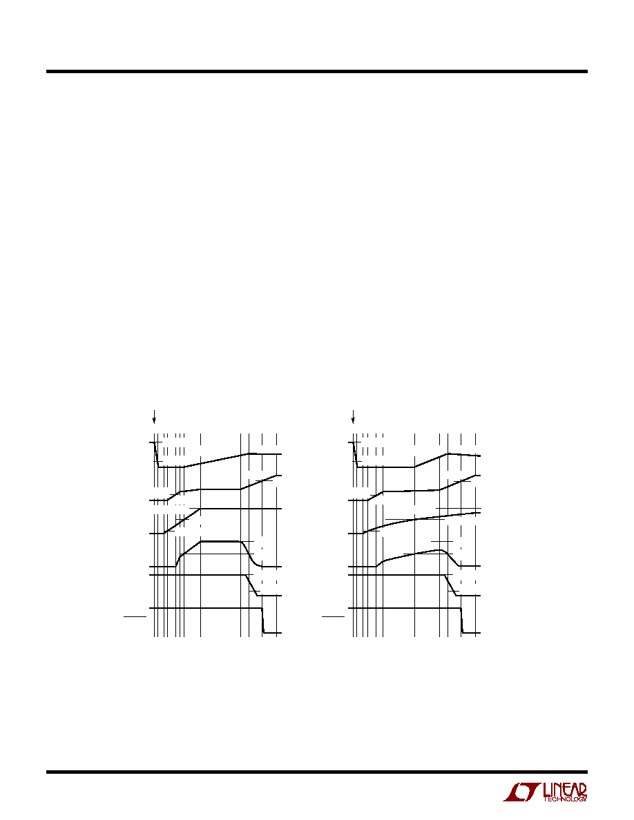
LTC4252-1/LTC4252-2
28
425212f
Soft-Start
If the SS pin is not connected, this pin defaults to a linear
voltage ramp, from 0V to 2.2V in about 220
µ
s at GATE
start-up, as shown in Figure 17a. If a soft-start capacitor,
C
SS
, is connected to this SS pin, the soft-start response is
modified from a linear ramp to an RC response (Equa-
tion 6), as shown in Figure 17b. This feature allows load
current to slowly ramp-up at GATE start-up. Soft-start is
initiated at time point 3 by a TIMER transition from V
TMRH
to V
TMRL
(time points 1 to 2) or by the OV pin falling below
the V
OVLO
threshold after an OV condition. When the SS
pin is below 0.2V, the analog current limit amplifier holds
GATE low. Above 0.2V, GATE is released and 58
µ
A ramps
up the compensation network and GATE capacitance at
time point 4. Meanwhile, the SS pin voltage continues to
ramp up. When GATE reaches the MOSFET's threshold,
the MOSFET begins to conduct. Due to the MOSFET's high
g
m
, the MOSFET current quickly reaches the soft-start
control value of V
ACL
(t) (Equation 7). At time point 6, the
GATE voltage is controlled by the current limit amplifier.
The soft-start control voltage reaches the circuit breaker
voltage, V
CB
, at time point 7 and the circuit breaker TIMER
activates. As the load capacitor nears full charge, load
current begins to decline below V
ACL
(t). The current limit
loop shuts off and GATE releases at time point 8. At time
point 9, the SENSE voltage falls below V
CB
and TIMER
deactivates.
Large values of C
SS
can cause premature circuit breaker
time out as V
ACL
(t) may exceed the V
CB
potential during
the circuit breaker delay. The load capacitor is unable to
achieve full charge in one GATE start-up cycle. A more
serious side effect of large C
SS
values is SOA duration may
be exceeded during soft-start into a low impedance load.
A soft-start voltage below V
CB
will not activate the circuit
breaker TIMER.
Figure 17. Soft-Start Timing (All Waveforms are Referenced to V
EE
)
(17a) Without External C
SS
(17b) With External C
SS
TIMER
GATE
SENSE
SS
DRAIN
V
TMRH
V
DRNCL
V
ACL
V
CB
V
DRNL
V
GS(th)
V
IN
≠ V
GATEH
V
TMRL
230
µ
A + 8 ∑ I
DRN
4252-1/2 F17
PWRGD
5.8
µ
A
58
µ
A
58
µ
A
TIMER
GATE
SENSE
SS
DRAIN
V
TMRH
V
DRNCL
V
CB
V
ACL
V
DRNL
V
GS(th)
V
IN
≠ V
GATEH
V
TMRL
230
µ
A + 8 ∑ I
DRN
PWRGD
5.8
µ
A
58
µ
A
58
µ
A
12 34 567
7a
8 9
10
11
END OF INTIAL TIMING CYCLE
12 3 4 5 6
7
8 9
10
11
END OF INTIAL TIMING CYCLE
20 ∑ V
OS
20 ∑ (V
CB
+ V
OS
)
20 ∑ (V
ACL
+ V
OS
)
20 ∑ V
OS
20 ∑ (V
CB
+ V
OS
)
20 ∑ (V
ACL
+ V
OS
)
APPLICATIO S I FOR ATIO
W
U
U
U
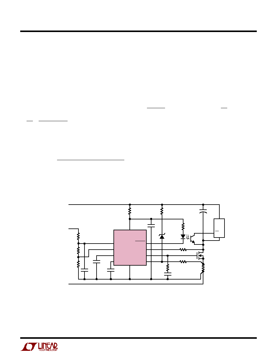
LTC4252-1/LTC4252-2
29
425212f
Figure 18. Power Limit Circuit Breaking Application
4252-1/2 F18
GND
UV
OV
V
EE
V
IN
SENSE
SS
TIMER
GATE
PWRGD
DRAIN
LTC4252-1
R1
432k
1%
R2
14k
1%
R3
32.4k
1%
C
SS
0.33
µ
F
C
T
68nF
C
C
18nF
≠48V
R
S
0.02
Q1
IRF530S
V
OUT
R
C
10
R5
5.6k
R4
31.6k
D1
BZX84C36
R
IN
3
◊
1.8k
1/4W EACH
1
9
8
10
3
2
7
6
4
5
C1
10nF
C
IN
1
µ
F
C
L
100
µ
F
GND
(SHORT PIN)
+
R
D
1M
R6 22
LOAD
EN
*
* M0C207
Power Limit Circuit Breaker
Figure 18 shows the LTC4252-2 in a power limit circuit
breaking application. The SENSE pin is modulated by the
board supply voltage, V
SUPPLY
. The zener voltage, V
Z
is set
to be the same as the low supply operating voltage,
V
SUPPLY(MIN)
= 36V. If the goal is to have the high supply
operating voltage, V
SUPPLY(MAX)
= 72V give the same
power at V
SUPPLY(MIN)
, then resistors R4 and R6 are
selected using the ratio:
R
R
V
V
CB
SUPPLY MAX
6
4
=
(
)
(16)
If R6 is 22
, R4 is 31.6k. The peak circuit breaker power
limit is:
POWER
V
V
V
V
POWER
POWER
MAX
SUPPLY MIN
SUPPLY MAX
SUPPLY MIN
SUPPLY MAX
SUPPLY MIN
SUPPLY MIN
=
+
(
)
=
(
)
(
)
(
)
(
)
(
)
(
)
∑
∑
∑
.
∑
2
4
1 125
(17)
when
V
SUPPLY
= 0.5 ∑ (V
SUPPLY(MIN)
+ V
SUPPLY(MAX)
) = 54V.
The peak power at the fault current limit occurs at the
supply overvoltage threshold. The fault current limited
power is:
POWER
V
R
V
V
V
R
R
FAULT
SUPPLY
S
ACL
SUPPLY
Z
=
(
)
∑
≠
≠
∑
6
4
(18)
APPLICATIO S I FOR ATIO
W
U
U
U

LTC4252-1/LTC4252-2
30
425212f
PACKAGE DESCRIPTIO
U
MS8 Package
8-Lead Plastic MSOP
(Reference LTC DWG # 05-08-1660)
MSOP (MS8) 1001
0.53
±
0.015
(.021
±
.006)
SEATING
PLANE
NOTE:
1. DIMENSIONS IN MILLIMETER/(INCH)
2. DRAWING NOT TO SCALE
3. DIMENSION DOES NOT INCLUDE MOLD FLASH, PROTRUSIONS OR GATE BURRS.
MOLD FLASH, PROTRUSIONS OR GATE BURRS SHALL NOT EXCEED 0.152mm (.006") PER SIDE
4. DIMENSION DOES NOT INCLUDE INTERLEAD FLASH OR PROTRUSIONS.
INTERLEAD FLASH OR PROTRUSIONS SHALL NOT EXCEED 0.152mm (.006") PER SIDE
5. LEAD COPLANARITY (BOTTOM OF LEADS AFTER FORMING) SHALL BE 0.102mm (.004") MAX
0.18
(.077)
0.254
(.010)
1.10
(.043)
MAX
0.22 ≠ 0.38
(.009 ≠ .015)
0.13
±
0.05
(.005
±
.002)
0.86
(.034)
REF
0.65
(.0256)
BCS
0
∞
≠ 6
∞
TYP
DETAIL "A"
DETAIL "A"
GAUGE PLANE
1
2
3
4
4.88
±
0.1
(.192
±
.004)
8
7 6 5
3.00
±
0.102
(.118
±
.004)
(NOTE 3)
3.00
±
0.102
(.118
±
.004)
NOTE 4
0.52
(.206)
REF
5.23
(.206)
MIN
3.2 ≠ 3.45
(.126 ≠ .136)
0.889
±
0.127
(.035
±
.005)
RECOMMENDED SOLDER PAD LAYOUT
0.42
±
0.04
(.0165
±
.0015)
TYP
0.65
(.0256)
BSC
LTC4252-1/LTC4252-2
31
425212f
MS Package
10-Lead Plastic MSOP
(Reference LTC DWG # 05-08-1661)
PACKAGE DESCRIPTIO
U
Information furnished by Linear Technology Corporation is believed to be accurate and reliable.
However, no responsibility is assumed for its use. Linear Technology Corporation makes no represen-
tation that the interconnection of its circuits as described herein will not infringe on existing patent rights.
MSOP (MS) 0402
0.53
±
0.01
(.021
±
.006)
SEATING
PLANE
0.18
(.007)
1.10
(.043)
MAX
0.17 ≠ 0.27
(.007 ≠ .011)
0.13
±
0.05
(.005
±
.002)
0.86
(.034)
REF
0.50
(.0197)
TYP
1 2 3 4 5
4.88
±
0.10
(.192
±
.004)
0.497
±
0.076
(.0196
±
.003)
REF
8
9
10
7 6
3.00
±
0.102
(.118
±
.004)
(NOTE 3)
3.00
±
0.102
(.118
±
.004)
NOTE 4
NOTE:
1. DIMENSIONS IN MILLIMETER/(INCH)
2. DRAWING NOT TO SCALE
3. DIMENSION DOES NOT INCLUDE MOLD FLASH, PROTRUSIONS OR GATE BURRS.
MOLD FLASH, PROTRUSIONS OR GATE BURRS SHALL NOT EXCEED 0.152mm (.006") PER SIDE
4. DIMENSION DOES NOT INCLUDE INTERLEAD FLASH OR PROTRUSIONS.
INTERLEAD FLASH OR PROTRUSIONS SHALL NOT EXCEED 0.152mm (.006") PER SIDE
5. LEAD COPLANARITY (BOTTOM OF LEADS AFTER FORMING) SHALL BE 0.102mm (.004") MAX
0.254
(.010)
0
∞
≠ 6
∞
TYP
DETAIL "A"
DETAIL "A"
GAUGE PLANE
5.23
(.206)
MIN
3.2 ≠ 3.45
(.126 ≠ .136)
0.889
±
0.127
(.035
±
.005)
RECOMMENDED SOLDER PAD LAYOUT
0.305
±
0.038
(.0120
±
.0015)
TYP
0.50
(.0197)
BSC
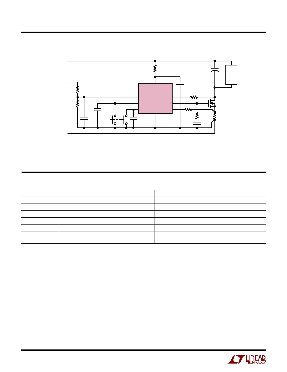
LTC4252-1/LTC4252-2
32
425212f
Linear Technology Corporation
1630 McCarthy Blvd., Milpitas, CA 95035-7417
(408) 432-1900
q
FAX: (408) 434-0507
q
www.linear.com
©
LINEAR TECHNOLOGY CORPORATION 2001
LT/TP 0702 2K PRINTED IN USA
RELATED PARTS
TYPICAL APPLICATIO
U
PART NUMBER
DESCRIPTION
COMMENTS
LT1640AH/LT1640AL
Negative High Voltage Hot Swap Controllers in SO-8
Negative High Voltage Supplies from ≠10V to ≠ 80V
LT1641-1/LT1641-2
Positive High Voltage Hot Swap Controllers in SO-8
Supplies from 9V to 80V, Latched Off/Autoretry
LTC1642
Fault Protected Hot Swap Controller
3V to 16.5V, Overvoltage Protection up to 33V
LT4250
≠ 48V Hot Swap Controller in SO-8
Active Current Limiting, Supplies from ≠ 20V to ≠ 80V
LTC4251/LTC4251-1
≠ 48V Hot Swap Controllers in SOT-23
Fast Active Current Limiting, Supplies from ≠15V
LTC4253
≠48V Hot Swap Controller with Sequencer
Fast Current Limiting with Three Sequenced Power Good Outputs,
Supplies from ≠15V
4252-1/2 F19
GND
UV/OV
V
EE
V
IN
SENSE
SS
TIMER
GATE
DRAIN
LTC4252-1
R1
402k
1%
R2
32.4k
1%
C
T
150nF
PUSH
RESET
C
SS
27nF
C
C
22nF
≠48V
R
S
0.01
Q1
IRF540S
V
OUT
R
C
10
R
IN
2
◊
5.1k IN SERIES
1/4W EACH
1
7
8
2
6
5
3
4
C1
10nF
C
IN
1
µ
F
C
L
100
µ
F
GND
(SHORT PIN)
+
R
D
1M
R3
22
LOAD
Figure 19. ≠ 48V/5A Application