4257f.pm6

LTC4257
1
4257f
The LTC
®
4257 provides complete signature and power
interface functions for a device operating in an IEEE
802.3af Power Over Ethernet system. The LTC4257 sim-
plifies Powered Device (PD) design by incorporating the
25k signature resistor, the classification current source,
inrush current limit, undervoltage lockout, thermal cur-
rent limit and power good signalling, all in a single 8-pin
package. By incorporating a high voltage power MOSFET
onboard, the LTC4257 provides the system designer with
reduced cost while also saving board space.
The LTC4257 can interface directly with a variety of Linear
Technology DC/DC converter products to provide a cost
effective power solution for IP phones, wireless access
points and other PDs. Linear Technology also provides
solutions for Power Sourcing Equipment (PSE) applica-
tions with quad network power controllers.
The LTC4257 is available in the 8-pin SO package.
s
IP Phone Power Management
s
Wireless Access Points
s
Telecom Power Control
, LTC and LT are registered trademarks of Linear Technology Corporation.
s
Complete Power Interface Port for IEEE 802.3af
®
Powered Devices (PDs)
s
Onboard 100V, 400mA Power MOSFET
s
Precision Inrush Current Limit
s
Onboard 25k Signature Resistor
s
Programmable Classification Current (Class 1-4)
s
Undervoltage Lockout
s
Smart Thermal Protection
s
Power Good Signal
s
Available in 8-Pin SO Package
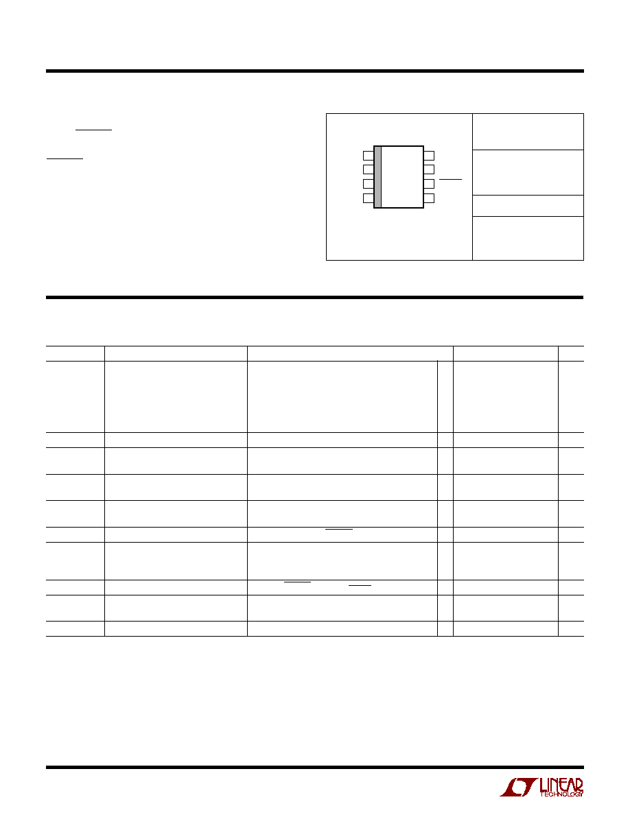
IEEE 802.3af PD
Power Over Ethernet
Interface Controller
GND
R
CLASS
R
CLASS
SMAJ58A
PWRGD
LTC4257
V
IN
SHDN
C1
100k
3.3V
TO LOGIC
RTN
SWITCHING
POWER SUPPLY
V
IN
V
OUT
48V FROM
POWER SOURCING
EQUIPMENT
(PSE)
4257 TA01
+
+
BR1
DF01SA
~
~
+
Powered Device (PD)
5ms/DIV
V
IN
50V/DIV
V
OUT
20V/DIV
I
IN
200mA/DIV
PWRGD
50V/DIV
4225 TA02
LTC4257 Charging 300
µ
F
Load Capacitor
FEATURES
DESCRIPTIO
U
APPLICATIO S
U
TYPICAL APPLICATIO
U
802 is a registered trademark of Institute of Electrical and Electronics Engineers, Inc.
LTC4257
2
4257f
SYMBOL
PARAMETER
CONDITIONS
MIN
TYP
MAX
UNITS
V
IN
Supply Voltage
Voltage with Respect to GND Pin (Notes 4, 5, 6)
Maximum Operating Voltage
q
57
V
Signature Range
q
1.5
9.5
V
Classification Range
q
12.5
21
V
UVLO Turn-On Voltage
q
37.7
39.2
40.2
V
UVLO Turn-Off Voltage
q
29.3
30.5
31.5
V
I
IN_ON
IC Supply Current when ON
V
IN
= 48V, Pins 5, 6 Floating
q
3
mA
I
IN_CLASS
IC Supply Current During Classification V
IN
= 17.5V, Pin 2 Floating, V
OUT
Tied to GND
q
0.35
0.50
0.65
mA
(Note 7)
I
CLASS
Current Accuracy During Classification 10mA < I
CLASS
< 40mA, 12.5V
V
IN
21V,
q
±
3.5
%
(Note 8)
R
SIGNATURE
Signature Resistance
1.5V
V
IN
9.5V, V
OUT
Tied to GND,
q
23.25
26.00
k
IEEE 802.3af 2-Point Measurement (Notes 4, 5)
V
PG_OUT
Power Good Output Low Voltage
I = 1mA, V
IN
= 48V, PWRGD Referenced to V
IN
q
0.5
V
Power Good Trip Point
V
IN
= 48V, Voltage Between V
IN
and V
OUT
V
PG_THRES_FALL
V
OUT
Falling
q
1.3
1.5
1.7
V
V
PG_THRES_RISE
V
OUT
Rising
q
2.7
3.0
3.3
V
I
PG_LEAK
Power Good Leakage
V
IN
= 0V, PWRGD FET Off, V
PWRGD
= 57V
q
1
µ
A
R
ON
On-Resistance
I = 300mA, V
IN
= 48V, Measured from V
IN
to V
OUT
1.0
1.6
q
2.0
I
OUT_LEAK
V
OUT
Leakage
V
IN
= 0V, Power MOSFET Off, V
OUT
= 57V (Note 9)
q
150
µ
A
(Notes 1, 2)
V
IN
Voltage ............................................. 0.3V to 100V
V
OUT
, PWRGD Voltage ............. V
IN
+ 100V to V
IN
0.3V
R
CLASS
Voltage ............................ V
IN
+ 7V to V
IN
0.3V
PWRGD Current .................................................. 40mA
R
CLASS
Current .................................................. 100mA
Operating Ambient Temperature Range ....... 0
°
C to 70
°
C
Junction Temperature ........................................... 150
°
C
Storage Temperature Range ................. 65
°
C to 150
°
C
Lead Temperature (Soldering, 10 sec).................. 300
°
C
Consult LTC Marketing for parts specified with wider operating temperature ranges.
The
q
denotes the specifications which apply over the full operating
temperature range, otherwise specifications are at T
A
= 25
°
C. (Note 3)
ORDER PART
NUMBER
S8 PART MARKING
T
JMAX
= 150
°
C,
JA
= 150
°
C/W
4257
LTC4257CS8
1
2
3
4
8
7
6
5
TOP VIEW
GND
NC
PWRGD
V
OUT
NC
R
CLASS
NC
V
IN
S8 PACKAGE
8-LEAD PLASTIC SO
PACKAGE/ORDER I FOR ATIO
U
U
W
ABSOLUTE AXI U RATI GS
W
W
W
U
ELECTRICAL CHARACTERISTICS
LTC4257
3
4257f
SYMBOL
PARAMETER
CONDITIONS
MIN
TYP
MAX
UNITS
The
q
denotes the specifications which apply over the full operating
temperature range, otherwise specifications are at T
A
= 25
°
C. (Note 3)
Note 1: Absolute Maximum Ratings are those values beyond which the life
of a device may be impaired.
Note 2: All voltages are with respect to GND pin.
Note 3: The LTC4257 operates with a negative supply voltage in the range
of 1.5V to 57V. To avoid confusion, voltages in this data sheet are
always referred to in terms of absolute magnitude. Terms such as
"maximum negative voltage" refer to the largest negative voltage and a
"rising negative voltage" refers to a voltage that is becoming more
negative.
Note 4: The LTC4257 is designed to work with two polarity protection
diodes between the PSE and PD. Parameter ranges specified in the
Electrical Characteristics are with respect to LTC4257 pins and are
designed to meet IEEE 802.3af specifications when these diode drops are
included. See Applications Information.
Note 5: Signature resistance is measured via the 2-point
V/
I method as
defined by IEEE 802.3af. The LTC4257 signature resistance is offset from
25k to account for diode resistance. With two series diodes, the total PD
resistance will be between 23.75k and 26.25k and meet IEEE 802.3af
specifications. The minimum probe voltages measured at the LTC4257
pins are 1.5V and 2.5V. The maximum probe voltages are 8.5V and
9.5V.
Note 6: The LTC4257 includes hysteresis in the UVLO voltages to preclude
any start-up oscillation. Per IEEE 802.3af requirements, the LTC4257 will
power up from a voltage source with 20
series resistance on the first
trial.
Note 7: I
IN_CLASS
does not include classification current programmed at
Pin 2. Total supply current in classification mode will be I
IN_CLASS
+ I
CLASS
(see Note 8).
Note 8: I
CLASS
is the measured current flowing through R
CLASS
.
I
CLASS
accuracy is with respect to the ideal current defined as
I
CLASS
= 1.237/R
CLASS
. The current accuracy specification does not
include variations in R
CLASS
resistance. The total classification current for
a PD also includes the IC quiescent current (I
IN_CLASS
). See Applications
Information.
Note 9: I
OUT_LEAK
includes current drawn at the V
OUT
pin by the power
good status circuit. This current is compensated for in the 25k
signature
resistance and does not affect PD operation.
Note 10: The LTC4257 includes smart thermal protection. In the event of
an overtemperature condition, the LTC4257 will reduce the inrush current
limit by 50% to reduce the power dissipation in the package. If the part
continues heating and reaches the shutdown temperature, the current is
reduced to zero until the part cools below the overtemperature limit. The
LTC4257 is also protected against thermal damage from incorrect
classification probing by the PSE. If the LTC4257 exceeds the
overtemperature trip point, the classification load current is disabled.
ELECTRICAL CHARACTERISTICS
I
LIMIT
Inrush Current Limit
V
IN
= 48V, V
OUT
= 43V (Note 10)
q
300
350
400
mA
I
LIMIT_WARM
Overtemperature Inrush Current Limit
(Note 10)
188
mA
T
OVERTEMP
Overtemperature Trip Temperature
(Note 10)
120
°
C
T
SHUTDOWN
Thermal Shutdown Trip Temperature
(Note 10)
140
°
C
LTC4257
4
4257f
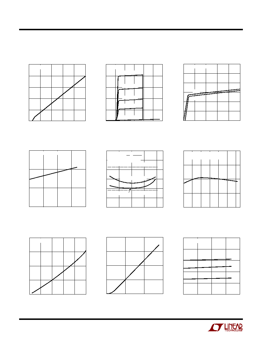
Input Current vs Input Voltage
INPUT VOLTAGE (V)
0
INPUT CURRENT (mA)
1
2
3
45
55
4257 G04
60
40
50
EXCLUDES ANY LOAD CURRENT
T
A
= 25
°
C
Normalized UVLO Threshold
vs Temperature
TYPICAL PERFOR A CE CHARACTERISTICS
U
W
V
OUT
Leakage Current
Input Current vs Input Voltage
INPUT VOLTAGE (V)
0
0
INPUT CURRENT (mA)
10
20
30
40
50
10
20
30
40
4257 G01
50
60
CLASS 4
CLASS 3
CLASS 2
CLASS 1
CLASS 0
T
A
= 25
°
C
INPUT VOLTAGE (V)
0
0
INPUT CURRENT (mA)
0.1
0.2
0.3
0.4
0.5
2
4
6
8
4357 G02
10
T
A
= 25
°
C
INPUT VOLTAGE (V)
12
9.0
INPUT CURRENT (mA)
9.5
10.5
11.0
11.5
14
16
4257 G03
10.0
18
20
22
12.0
85
°
C
40
°
C
CLASS 1 OPERATION
Input Current vs Input Voltage
25k Detection Range
Input Current vs Input Voltage
INPUT VOLTAGE (V)
1
22
V1:
V2:
SIGNATURE RESISTANCE (k
)
23
25
26
27
3
5
4257 G05
24
7
9
6
10
2
4
8
28
RESISTANCE =
DIODES: S1B
T
A
= 25
°
C
=
V
I
V2 V1
I
2
I
1
IEEE UPPER LIMIT
IEEE LOWER LIMIT
LTC4257 + 2 DIODES
LTC4257 ONLY
Signature Resistance
vs Input Voltage
TEMPERATURE (
°
C)
40
2
NORMALIZED UVLO THRESHOLD (%)
1
0
1
2
20
0
20
40
4257 G06
60
80
APPLICABLE TO TURN-ON
AND TURN-0FF THRESHOLDS
Power Good Output Low Voltage
vs Current
CURRENT (mA)
0
V
PG_OUT
(V)
2
3
8
4257 G07
1
0
2
4
6
10
4
T
A
= 25
°
C
V
OUT
PIN VOLTAGE (V)
0
0
V
OUT
CURRENT (
µ
A)
30
60
120
90
20
40
42571 G09
60
V
IN
= 0V
T
A
= 25
°
C
Current Limit vs Input Voltage
INPUT VOLTAGE (V)
40
CURRENT LIMIT (mA)
345
355
60
4257 G09
335
325
45
50
55
375
365
V
OUT
= V
IN
+ 5V
85
°
C
25
°
C
40
°
C
LTC4257
5
4257f
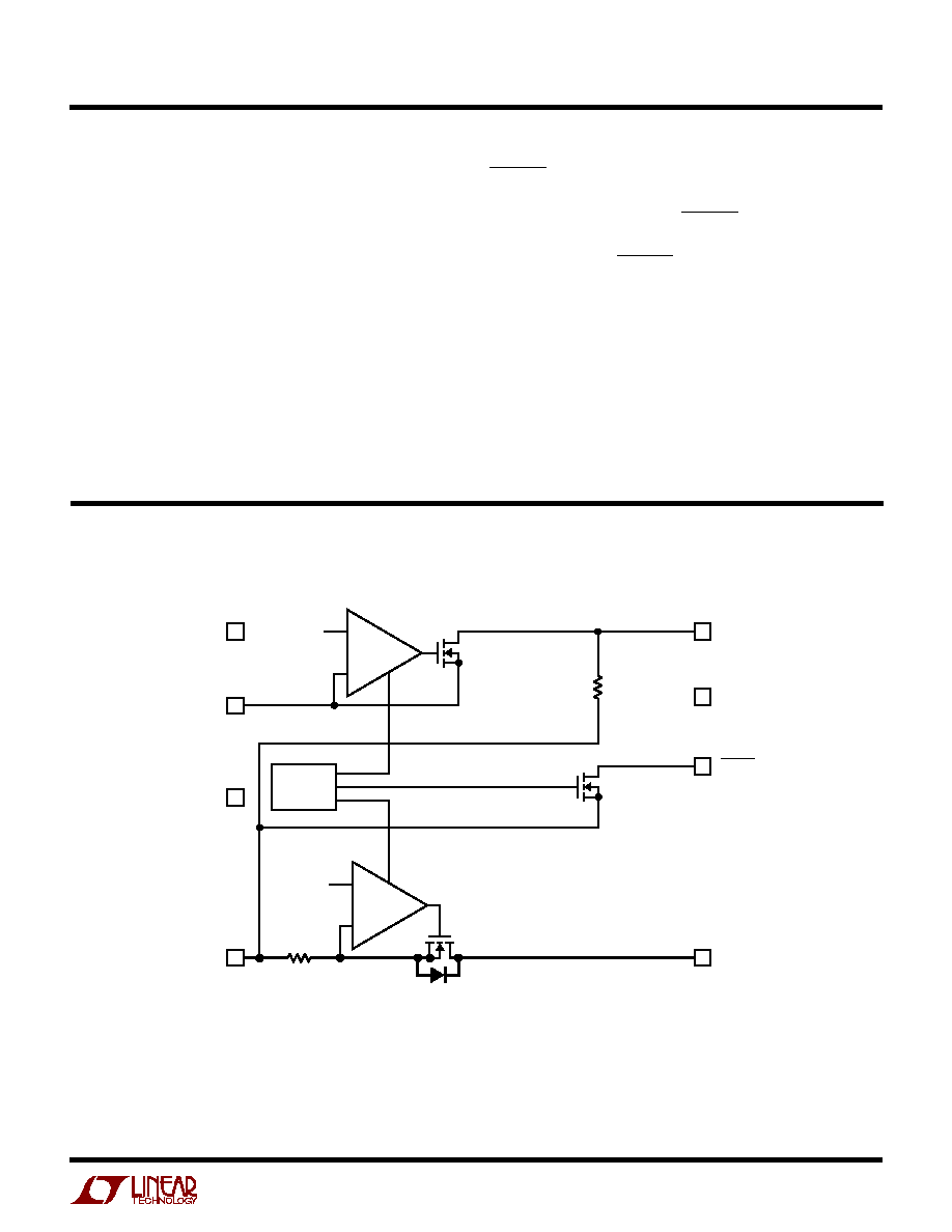
NC (Pin 1): No Connect.
R
CLASS
(Pin 2): External Class Select Input. Used to set the
current the LTC4257 maintains during classification. Con-
nect a resistor between R
CLASS
and V
IN
(see Table 2).
NC (Pin 3): No Connect.
V
IN
(Pin 4): Power Input. Tie to system 48V through the
input diode bridge.
V
OUT
(Pin 5): Power Output. Supplies 48V to the PD load
through an internal power MOSFET that limits inrush
current. V
OUT
is high impedance until the input voltage
rises above the turn-on UVLO threshold. Above the UVLO
threshold the output is current limited to 350mA.
PWRGD (Pin 6): Power Good Output, Open-Drain. Signals
that the LTC4257 MOSFET is fully on. Low impedance
indicates power is good. PWRGD is high impedance
during detection, classification and in the event of a
thermal overload. PWRGD is referenced to V
IN
.
NC (Pin 7): No Connect
GND (Pin 8): Ground. Tie to system ground and to power
return through the input diode bridge.
U
U
U
PI FU CTIO S
BLOCK DIAGRA
W
4257 BD
V
IN
BOLD LINE INDICATES HIGH CURRENT PATH
V
OUT
+
8
5
4
NC 3
R
CLASS
2
NC
PWRGD
GND
7
NC
1
6
CONTROL
CIRCUITS
INRUSH
CURRENT
LIMIT
70mV
POWER GOOD
CLASSIFICATION
CURRENT SOURCE
1.237V
EN
0.2
+
EN
25k SIGNATURE
RESISTOR