4261f.indd
LTC4261
1
4261f
Negative Voltage
Hot Swap Controller with
ADC and I
2
C Monitoring
The LTC
®
4261 negative voltage Hot Swap
TM
controller al-
lows a board to be safely inserted and removed from a live
backplane. Using an external N-channel pass transistor,
the board supply voltage can be ramped at an adjustable
rate. The device features independently adjustable inrush
current and overcurrent limits to minimize stresses on
the pass transistor during start-up, input step and output
short conditions.
An I
2
C interface and onboard 10-bit ADC allow monitoring
of board current, voltage and fault status. A single-wire
broadcast mode is available to simplify the interface by
eliminating two optoisolators.
The controller has additional features to interrupt the host
when a fault has occurred, notify when output power is
good, detect insertion of a board and turn off the pass
transistor if an external supply monitor fails to indicate
power good within a timeout period.
AdvancedTCA Systems
Telecom Infrastructure
48V Distributed Power Systems
Power Monitors
Allows Safe Insertion into Live 48V Backplanes
10-Bit ADC Monitors Current and Voltages
I
2
C/SMBus Interface or Single-Wire Broadcast Mode
Wide Operating Voltage Range: 12V to 100V
Independently Adjustable Inrush and Overcurrent
Limits
Controlled Soft-Start Inrush
Adjustable UV/OV Thresholds and Hysteresis
Sequenced Power Good Outputs with Delays
Adjustable Power Good Input Timeout
Programmable Latchoff or Auto-Retry After Faults
Alerts Host After Faults
Available in 28-Lead Narrow SSOP and 24-Lead
(4mm × 5mm) QFN Packages
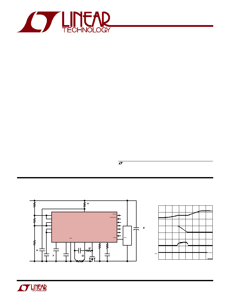
48V/200W Hot Swap Controller with I
2
C and ADC
APPLICATIO S
U
FEATURES
DESCRIPTIO
U
TYPICAL APPLICATIO
U
, LTC and LT are registered trademarks of Linear Technology Corporation.
Hot Swap is a trademark of Linear Technology Corporation. Patents pending.
All other trademarks are the property of their respective owners.
+
PGI
ALERT
SDAO
SDAI
SCL
ADIN
PGIO
PG
UVL
UVH
ADIN2
OV
INTV
CC
ON
RAMP
DRAIN
GATE
LTC4261CGN
V
IN
V
EE
EN
TMR
SS
SENSE
1M
4 1k IN SERIES
1/4W EACH
453k
1%
48V RTN
48V INPUT
UV = 38.5V
UV RELEASE
AT 43V
OV RELEASE
AT 71V
OV = 72.3V
16.9k
1%
11.8k
1%
10nF
100V
5%
47nF
0.1 F
1 F
220nF
47nF
0.008
1%
10
V
OUT
Q1
IRF1310NS
1k
330 F
100V
LOAD
ON
4261 TA01
V
IN
+
V
IN
Start-Up Behavior
4261 TA01b
20ms/DIV
GATE
10V/DIV
PG
50V/DIV
V
OUT
50V/DIV
SENSE
1A/DIV
LTC4261
2
4261f
V
IN
(Note 3) ......................................... 0.3V to 10.65V
Drain (Note 4) .......................................... 0.3V to 3.5V
PGI, ON, ALERT, SDAO, SDAI, SCL, ADIN, ADIN2,
OV, SENSE, ADR1, ADR0, FLTIN, TMR,
SS, RAMP Voltages .................... 0.3V to INTV
CC
+ 0.3V
UVL, UVH, EN ............................................ 0.3V to 10V
GATE Voltage .................................. 0.3V to V
IN
+ 0.3V
PG, PGIO Voltages .................................. 0.3V to 100V
Supply Voltage (INTV
CC
) .......................... 0.3V to 5.5V
(Notes 1, 2)
ABSOLUTE AXI U RATI GS
W
W
W
U
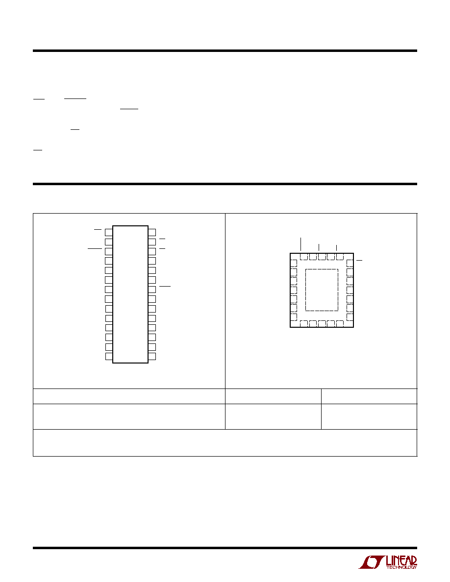
PACKAGE/ORDER I FOR ATIO
U
U
W
1
2
3
4
5
6
7
8
9
10
11
12
13
14
TOP VIEW
GN PACKAGE
28-LEAD PLASTIC SSOP
28
27
26
25
24
23
22
21
20
19
18
17
16
15
PGI
ON
ALERT
SDAO
SDAI
SCL
INTV
CC
UVL
UVH
ADIN2
OV
NC
V
EE
SENSE
PGIO
PG
EN
ADR1
ADR0
ADIN
FLTIN
V
IN
TMR
SS
RAMP
NC
DRAIN
GATE
T
JMAX
= 125°C,
JA
= 85°C/W
8
9
TOP VIEW
25
UFD PACKAGE
24-LEAD (4mm
× 5mm) PLASTIC QFN
10 11 12
24 23 22 21 20
6
5
4
3
2
1
SDAO
SDAI
SCL
INTV
CC
UVL
UVH
OV
EN
ADR1
ADR0
ADIN
V
IN
TMR
SS
ALERT
ON
PGI
PGIO
PG
V
EE
SENSE
GATE
DRAIN
RAMP
7
14
15
16
17
18
19
13
T
JMAX
= 125°C,
JA
= 45°C/W
EXPOSED PAD (PIN 25) PCB V
EE
ELECTRICAL CONNECTION OPTIONAL
ORDER PART NUMBER
ORDER PART NUMBER
UFD PART MARKING*
LTC4261CGN
LTC4261IGN
LTC4261CUFD
LTC4261IUFD
4261
4261
Order Options Tape and Reel: Add #TR
Lead Free: Add #PBF Lead Free Tape and Reel: Add #TRPBF
Lead Free Part Marking:
http://www.linear.com/leadfree/
*The temperature grade is identified by a label on the shipping container. Consult LTC Marketing for parts specified with wider operating temperature ranges.
Operating Temperature Range
LTC4261C ................................................ 0°C to 70°C
LTC4261I ............................................. 40°C to 85°C
Storage Temperature Range
SSOP ................................................. 65°C to 150°C
QFN .................................................... 65°C to 125°C
Lead Temperature (Soldering, 10 sec)
SSOP Only ........................................................ 300°C
LTC4261
3
4261f
The
denotes the specifications which apply over the full operating
temperature range, otherwise specifications are at I
IN
= 5mA, T
A
= 25°C. (Note 2)
SYMBOL
PARAMETER
CONDITIONS
MIN
TYP
MAX
UNITS
General
V
Z
Shunt Regulator Voltage at V
IN
I
IN
= 5mA
10.65
11.2
11.8
V
V
Z
Shunt Regulator Load Regulation
I
IN
= 5mA to 25mA
370
600
mV
I
IN
V
IN
Supply Current
V
IN
= V
Z
0.3V
2
5
mA
V
IN(UVLO)
V
IN
Undervoltage Lockout Threshold
V
IN
Rising
8.5
9
9.5
V
V
IN(UVLO)
V
IN
Undervoltage Lockout Hysteresis
0.3
0.7
1
V
INTV
CC
Internal Regulator Voltage
I
LOAD
= 1mA to 20mA, I
IN
= 25mA
4.75
5
5.25
V
Gate Drive
V
GATEH
GATE Pin Output High Voltage
V
IN
= 10.65V
10
10.25
10.5
V
I
GATE(UP)
GATE Pin Pull-Up Current
V
GATE
= 4V
7.5
11.5
15.5
µA
I
GATE(OFF)
GATE Turn-Off Current
V
SENSE
= 300mV, V
GATE
= 4V
60
110
140
mA
Gate Off, V
GATE
= 4V
60
110
140
mA
t
PHL(SENSE)
SENSE High to Current Limit
V
SENSE
= 100mV, C
GATE
= 1pF
0.5
1.5
µs
Propagation Delay
V
SENSE
= 300mV, C
GATE
= 1pF
0.2
0.5
µs
t
PHL(GATE)
GATE Off Propagation Delay
Input High (OV, EN, PGI), Input Low (ON, UVL),
C
GATE
= 1pF
0.2
0.5
µs
t
PHLCB
Circuit Breaker Gate Off Delay
V
GATE
< 2V, C
GATE
= 1pF
440
530
620
µs
I
RAMP
RAMP Pin Current
V
SS
= 2.56V
18
20
22
µA
V
SS
SS Pin Clamp Voltage
2.43
2.56
2.69
V
I
SS(UP)
SS Pin Pull-Up Current
V
SS
= 0V
7
10
13
µA
I
SS(DN)
SS Pin Pull-Down Current
V
SS
= 2.56V
6
12
20
mA
Input Pins
V
UVH(TH)
UVH Threshold Voltage
V
UVH
Rising
LTC4261C
LTC4261I
2.528
2.514
2.56
2.56
2.592
2.606
V
V
UVL(TH)
UVL Threshold Voltage
V
UVL
Falling
LTC4261C
LTC4261I
2.262
2.250
2.291
2.291
2.320
2.332
V
V
UV(HYST)
Built-In UV Hystersis
UVH and UVL Tied Together
256
269
282
mV
V
UV
UVH, UVL Minimum Hysteresis
15
mV
V
UVLR(TH)
UVL Reset Threshold Voltage
V
UVL
Falling
1.12
1.21
1.30
V
V
UVLR(HYST)
UVL Reset Hysteresis
60
mV
V
OV(TH)
OV Pin Threshold Voltage
V
OV
Rising
LTC4261C
LTC4261I
1.743
1.730
1.770
1.770
1.797
1.810
V
V
OV(HYST)
OV Pin Hysteresis
18
37.5
62
mV
V
SENSE
Current Limit Sense Voltage Threshold V
SENSE
V
EE
45
50
55
mV
V
INPUT(TH)
ON, EN, PGI, FLTIN Threshold Voltage
ON, EN, PGI, FLTIN Falling or Rising
0.8
1.4
2
V
V
INPUT(HYST)
ON, EN, PGI, FLTIN Hysteresis
170
mV
V
PGIO(TH)
PGIO Pin Input Threshold Voltage
V
PGIO
Rising
1.10
1.25
1.40
V
V
PGIO(HYST)
PGIO Pin Input Hysteresis
100
mV
I
INPUT
ON, EN, UVH, UVL, OV, SENSE, PGI,
FLTIN Input Current
ON, EN, UVH, UVL, OV, SENSE, PGI, FLTIN = 3V
0
±2
µA
ELECTRICAL CHARACTERISTICS
LTC4261
4
4261f
SYMBOL
PARAMETER
CONDITIONS
MIN
TYP
MAX
UNITS
Timer
V
TMR(H)
TMR Pin High Threshold
V
TMR
Rising
2.43
2.56
2.69
V
V
TMR(L)
TMR Pin Low Threshold
V
TMR
Falling
40
75
110
mV
I
TMR(UP)
TMR Pin Pull-Up Current
Turn-On and Auto-Retry (Except OC) Delays,
V
TMR
= 0.2V
7
10
13
µA
Power Good, PGI Check and OC Auto-Retry
Delays, V
TMR
= 0.2V
3.5
5
6.5
µA
I
TMR(DN)
TMR Pin Pull-Down Current
Delays Except PGI Check or OC Auto-Retry,
V
TMR
= 2.56V
6
12
20
mA
PGI Check and OC Auto-Retry Delays,
V
TRM
= 2.56V
3
5
7
µA
Output Pins
V
PWRGD
PG, PGIO Pins Output Low
I
PG
, I
PGIO
= 3mA
I
PG
, I
PGIO
= 500µA
0.8
0.15
1.6
0.4
V
V
I
PWRGD
PG, PGIO Pins Leakage Current
PG, PGIO = 80V
0
±10
µA
ADC
Resolution (No Missing Codes)
(Note 5)
10
Bits
INL
Integral Nonlinearity
SENSE
2.5
2.5
LSB
ADIN2/OV, ADIN
1.25
1.25
LSB
V
OS
Offset Error
SENSE
1.75
1.75
LSB
ADIN2/OV, ADIN
1.25
1.25
LSB
Full-Scale Voltage
SENSE
62.8
64
65.2
mV
ADIN2/0V, ADIN
2.514
2.560
2.606
V
Conversion Rate
5.5
7.3
9
Hz
R
ADIN
ADIN, ADIN2 Pins Input Resistance
ADIN, ADIN2 = 1.28V
2
10
M
I
ADIN
ADIN, ADIN2 Pins Input Current
ADIN, ADIN2 = 2.56V
0
±2
µA
I
2
C Interface
V
ADR(H)
ADR0, ADR1 Input High Threshold
INTV
CC
0.8
INTV
CC
0.5
INTV
CC
0.3
V
V
ADR(L)
ADR0, ADR1 Input Low Threshold
0.3
0.5
0.8
V
I
ADR(IN,HL)
ADR0, ADR1 High, Low Input Current
ADR0, ADR1 = 0V, 5V
±80
µA
I
ADR(IN,Z)
ADR0, ADR1 Hi-Z Input Current
ADR0, ADR1 = 0.8V, (INTV
CC
0.8V)
±10
µA
V
ALERT(OL)
ALERT Pin Output Low Voltage
I
ALERT
= 4mA
0.2
0.4
V
V
SDAO(OL)
SDAO Pin Output Low Voltage
I
SDAO
= 4mA
0.2
0.4
V
I
SDAO,ALERT(IN)
SDAO, ALERT Input Current
SDAO, ALERT = 5V
0
±5
µA
V
SDAI,SCL(TH)
SDAI, SCL Input Threshold
1.6
1.8
2
V
I
SDAI,SCL(IN)
SDAI, SCL Input Current
SDAI, SCL = 5V
0
±2
µA
The
denotes the specifications which apply over the full operating
temperature range, otherwise specifications are at I
IN
= 5mA, T
A
= 25°C. (Note 2)
ELECTRICAL CHARACTERISTICS
LTC4261
5
4261f
SYMBOL
PARAMETER
CONDITIONS
MIN
TYP
MAX
UNITS
I
2
C Interface Timing (Note 5)
f
SCL(MAX)
Maximum SCL Clock Frequency
400
kHz
t
LOW
SCL Low Period
0.65
1.3
µs
t
HIGH
SCL High Period
50
600
ns
t
BUF(MIN)
Minimum Bus Free Time Between
Stop/Start Condition
0.12
1.3
µs
t
HD,STA(MIN)
Minimum Hold Time After (Repeated)
Start Condition
140
600
ns
t
SU,STA(MIN)
Minimum Repeated Start Condition
Set-Up Time
30
600
ns
t
SU,STO(MIN)
Minimum Stop Condition Set-Up Time
30
600
ns
t
HD,DATI(MIN)
Minimum Data Hold Time Input
100
0
ns
t
HD,DATO(MIN)
Minimum Data Hold Time Output
300
600
900
ns
t
SU,DAT(MIN)
Minimum Data Set-Up Time Input
30
100
ns
t
SP(MAX)
Maximum Suppressed Spike Pulse
Width
50
110
250
ns
t
RST
Stuck-Bus Reset Time
SCL or SDAI Held Low
25
66
ms
C
X
SCL,SDA Input Capacitance
SDAI Tied to SDAO
5
10
pF
The
denotes the specifications which apply over the full operating
temperature range, otherwise specifications are at I
IN
= 5mA, T
A
= 25°C. (Note 2)
ELECTRICAL CHARACTERISTICS
Note 1: Absolute Maximum Ratings are those values beyond which the life
of a device may be impaired.
Note 2: All currents into pins are positive, all voltages are referenced to
device GND (V
EE
) unless otherwise specified.
Note 3: An internal shunt regulator limits the V
IN
pin to a minimum of
10.65V. Driving this pin to voltages beyond 10.65V may damage the part.
The pin can be safely tied to higher voltages through a resistor that limits
the current below 50mA.
Note 4: An internal clamp limits the DRAIN pin to a minimum of 3.5V.
Driving this pin to voltages beyond the clamp may damage the part. The
pin can be safely tied to higher voltages through a resistor that limits the
current below 2mA.
Note 5: Guaranteed by design and not subject to test.