1
LTC4301
4301fa
FEATURES
DESCRIPTIO
U
APPLICATIO S
U
TYPICAL APPLICATIO
U
Supply Independent Hot
Swappable 2-Wire Bus Buffer
s
Allows Bus Pull-Up Voltages Above or Below V
CC
s
Bidirectional Buffer* for SDA and SCL Lines
Increases Fanout
s
Prevents SDA and SCL Corruption During Live Board
Insertion and Removal from Backplane
s
Isolates Input SDA and SCL Line from Output
s
10kV Human Body Model ESD Protection
s
1V Precharge On All SDA and SCL Lines
s
Supports Clock Stretching, Arbitration and
Synchronization
s
High Impedance SDA, SCL Pins for V
CC
= 0V
s
CS Gates Connection from Input to Output
s
Compatible with I
2
C
TM
, I
2
C Fast Mode and SMBus
Standards (Up to 400kHz Operation)
s
Small 8-Pin MSOP and DFN (3mm
◊
3mm) Packages
s
Hot Board Insertion
s
Servers
s
Capacitance Buffer/Bus Extender
s
Desktop Computers
s
CompactPCI
TM
and ATCA Systems
, LTC and LT are registered trademarks of Linear Technology Corporation.
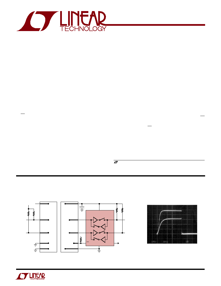
The LTC
Æ
4301 supply independent, hot swappable, 2-wire
bus buffer allows I/O card insertion into a live backplane
without corruption of the data and clock busses. In addi-
tion, the LTC4301 allows the V
CC
, SDAIN and SCLIN pull-
up voltage and the SDAOUT and SCLOUT pull-up voltage
to be independent from each other. Control circuitry
prevents the backplane from being connected to the card
until a stop bit or a bus idle is present. When the connec-
tion is made, the LTC4301 provides bidirectional buffer-
ing, keeping the backplane and card capacitances isolated.
During insertion, the SDA and SCL lines are precharged to
1V to minimize bus disturbances. When driven low, the CS
input pin allows the part to connect after a stop bit or bus
idle occurs. Driving CS high breaks the connection be-
tween SCLIN and SCLOUT and between SDAIN and
SDAOUT. The READY output pin indicates that the back-
plane and card sides are connected together.
The LTC4301 is offered in 8-pin DFN (3mm
◊
3mm) and
MSOP packages.
10k
10k
5V
BACK_SCL
BACKPLANE
CONNECTOR
CARD
BACK_SDA
3.3V
10k
5V
CS
CARD_SCL
CARD_SDA
SCLOUT
SCLIN
SDAOUT
SDAIN
GND
V
CC
LTC4301
READY
0.01
µ
F
4301 TA01
10k
10k
ST
AGGERED CONNECTOR
Input-Output Connection
4301 TA01b
OUTPUT
SIDE
20pF
INPUT
SIDE
55pF
1
µ
s/DIV
1V/DIV
I
2
C is a trademark of Philips Electronics N.V.
CompactPCI is a trademark of the PCI Industrial Computer Manufacturers Group.
*Patent Pending
2
LTC4301
4301fa
ORDER PART
NUMBER
V
CC
to GND ................................................. ≠0.3V to 7V
SDAIN, SCLIN, SDAOUT, SCLOUT, CS ........ ≠0.3V to 7V
READY ........................................................ ≠0.3V to 6V
Operating Temperature Range
LTC4301C ............................................... 0
∞
C to 70
∞
C
LTC4301I ............................................ ≠ 40
∞
C to 85
∞
C
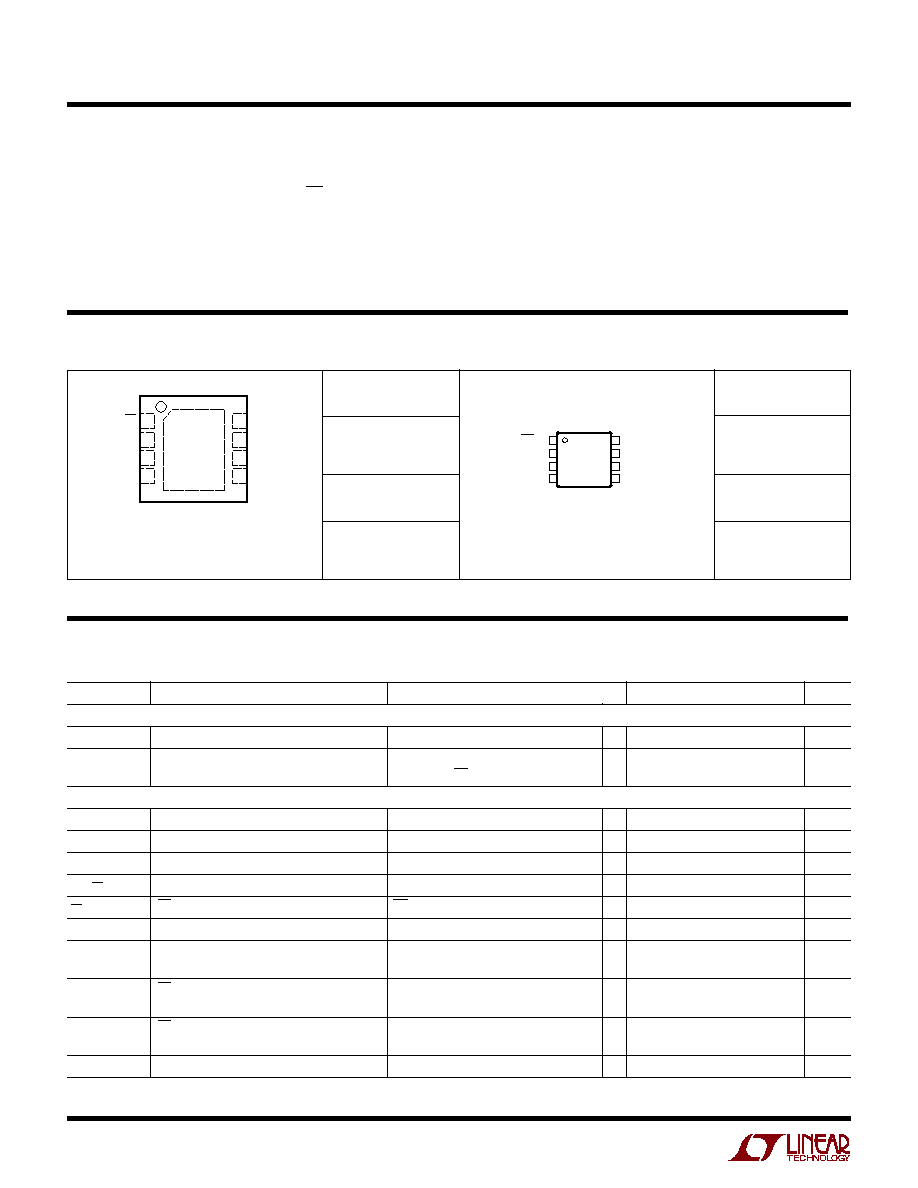
LTC4301CDD
LTC4301IDD
T
JMAX
= 125
∞
C,
JA
= 43
∞
C/W
EXPOSED PAD (PIN 9)
PCB CONNECTION OPTIONAL
ABSOLUTE
M
AXI
M
U
M
RATINGS
W
W
W
U
PACKAGE/ORDER I
N
FOR
M
ATIO
N
W
U
U
DD PART
MARKING*
LBBY
*The temperature grade is identified by a label on the shipping container. Consult LTC Marketing for parts specified with wider operating temperature ranges.
Storage Temperature Range
MSOP ............................................... ≠ 65
∞
C to 150
∞
C
DFN .................................................. ≠ 65
∞
C to 125
∞
C
Lead Temperature (Soldering, 10 sec).................. 300
∞
C
(Note 1)
ORDER PART
NUMBER
LTC4301CMS8
LTC4301IMS8
MS8 PART
MARKING*
LTBBW
TOP VIEW
9
DD PACKAGE
8-LEAD (3mm
◊
3mm) PLASTIC DFN
5
6
7
8
4
3
2
1
CS
SCLOUT
SCLIN
GND
V
CC
SDAOUT
SDAIN
READY
T
JMAX
= 125
∞
C,
JA
= 200
∞
C/W
1
2
3
4
CS
SCLOUT
SCLIN
GND
8
7
6
5
V
CC
SDAOUT
SDAIN
READY
TOP VIEW
MS8 PACKAGE
8-LEAD PLASTIC MSOP
The
q
indicates specifications which apply over the full operating
temperature range, otherwise specifications are at T
A
= 25
∞
C. V
CC
= 2.7V to 5.5V, unless otherwise noted.
ELECTRICAL CHARACTERISTICS
SYMBOL
PARAMETER
CONDITIONS
MIN
TYP
MAX
UNITS
Power Supply
V
CC
Positive Supply Voltage
q
2.7
5.5
V
I
CC
Supply Current
V
CC
= 5.5V, V
SDAIN
= V
SCLIN
= 0V
q
4.5
6.2
mA
V
CC
= 5.5V, CS = 5.5V
300
µ
A
Start-Up Circuitry
V
PRE
Precharge Voltage
SDA, SCL Floating
q
0.85
1.05
1.25
V
t
IDLE
Bus Idle Time
q
60
95
175
µ
s
RDY
VOL
READY Output Low Voltage
I
PULLUP
= 3mA
q
0.4
V
V
THRCS
Connection Sense Threshold
0.8
1.4
2
V
I
CS
CS Input Current
CS from 0V to V
CC
±
0.1
±
1
µ
A
V
THR
SDA, SCL Logic Input Threshold Voltage
Rising Edge
1.55
1.8
2.0
V
V
HYS
SDA, SCL Logic Input Threshold Voltage
(Note 3)
50
mV
Hysteresis
t
PLH
CS Delay On-Off
10
ns
READY Delay Off-On
10
ns
t
PHL
CS Delay Off-On
95
µ
s
READY Delay On-Off
10
ns
I
OFF
Ready Off Leakage Current
±
0.1
µ
A
3
LTC4301
4301fa
The
q
indicates specifications which apply over the full operating
temperature range, otherwise specifications are at T
A
= 25
∞
C. V
CC
= 2.7V to 5.5V, unless otherwise noted.
ELECTRICAL CHARACTERISTICS
SYMBOL
PARAMETER
CONDITIONS
MIN
TYP
MAX
UNITS
Input-Output Connection
V
OS
Input-Output Offset Voltage
10k to V
CC
on SDA, SCL, V
CC
= 3.3V,
q
0
100
175
mV
SDA or SCL = 0.2V (Note 2)
C
IN
Digital Input Capacitance SDAIN, SDAOUT,
(Note 3)
10
pF
SCLIN, SCLOUT
I
LEAK
Input Leakage Current
SDA, SCL Pins
±
5
µ
A
V
OL
Output Low Voltage, Input = 0V
SDA, SCL Pins, I
SINK
= 3mA, V
CC
= 2.7V
q
0
0.4
V
Timing Characteristics
f
I2C,MAX
I
2
C Maximum Operating Frequency
(Note 3)
400
600
kHz
t
BUF
Bus Free Time Between Stop and Start
(Note 3)
1.3
µ
s
Condition
t
HD,STA
Hold Time After (Repeated) Start Condition
(Note 3)
100
ns
t
SU,STA
Repeated Start Condition Set-Up Time
(Note 3)
0
ns
t
SU,STO
Stop Condition Set-Up Time
(Note 3)
0
ns
t
HD,DATI
Data Hold Time Input
(Note 3)
0
ns
t
SU,DAT
Data Set-Up Time
(Note 3)
100
ns
Note 1: Absolute Maximum Ratings are those values beyond which the life
of a device may be impaired.
Note 2: The connection circuitry always regulates its output to a higher
voltage than its input. The magnitude of this offset voltage as a function of
the pull-up resistor and V
CC
voltage is shown in the Typical Performance
Characteristics section.
Note 3: Determined by design, not tested in production.
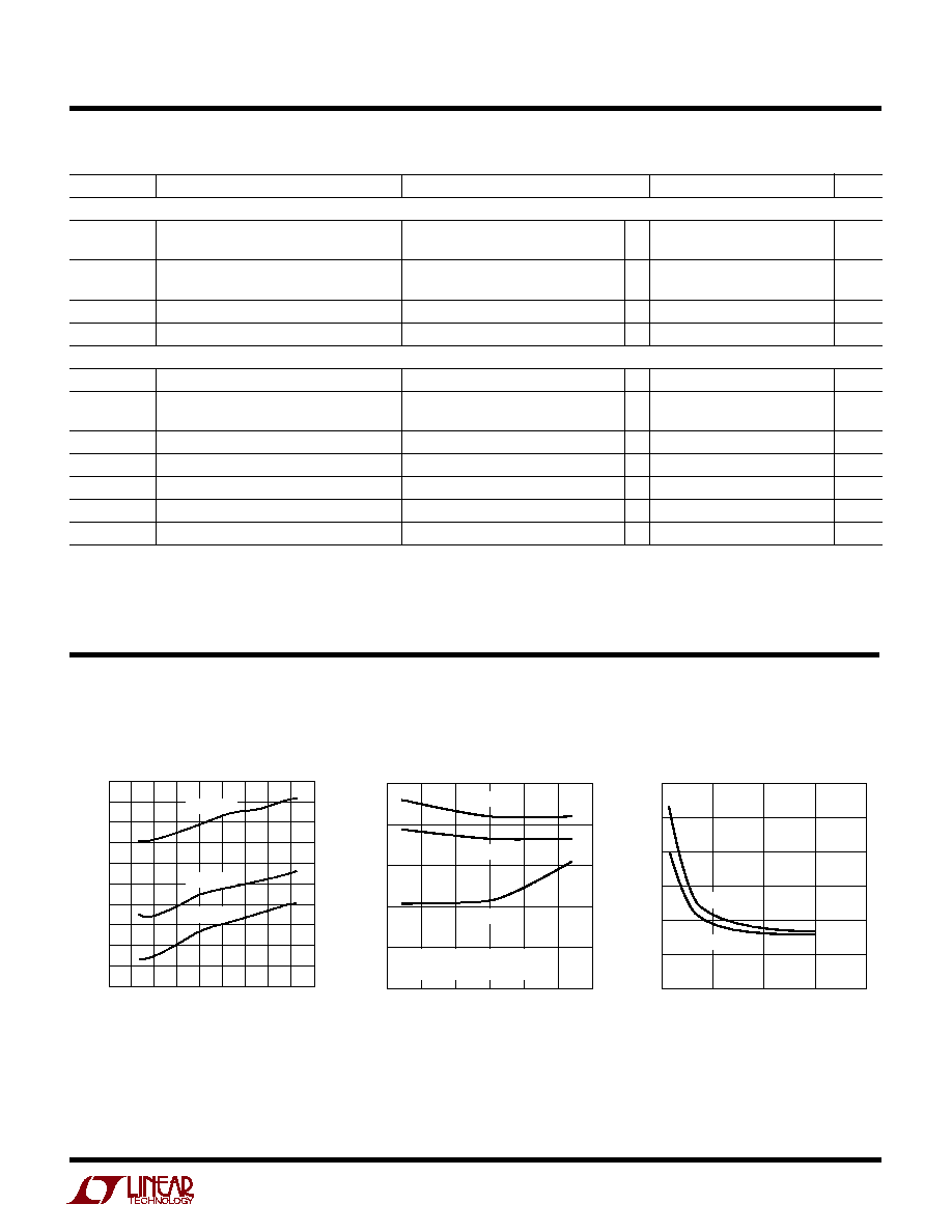
TYPICAL PERFOR A CE CHARACTERISTICS
U
W
I
CC
vs Temperature
Input ≠ Output High to Low
Propagation Delay vs Temperature
Connection Circuitry V
OUT
≠ V
IN
≠50
≠25
0
25
50
75
100
TEMPERATURE (
∞
C)
TIME (ns)
4301 G02
100
80
60
40
20
0
V
CC
= 2.7V
V
CC
= 3.3V
V
CC
= 5.5V
C
IN
= C
OUT
= 100pF
R
PULLUPIN
= R
PULLUPOUT
= 10k
R
PULLUP
(
)
0
10,000
20,000
30,000
40,000
V
OUT
≠ V
IN
(mV)
4301 G03
300
250
200
150
100
50
0
V
CC
= 3.3V
V
CC
= 5V
T
A
= 25
∞
C
V
IN
= 0V
TEMPERATURE (
∞
C)
≠80
I
CC
(mA)
4.9
4.8
4.7
4.6
4.5
4.4
4.3
4.2
4.1
4.0
3.9
≠40
0
20
100
4301 G01
≠60
≠20
40
60
80
V
CC
= 5.5V
V
CC
= 3.3V
V
CC
= 2.7V
4
LTC4301
4301fa
U
U
U
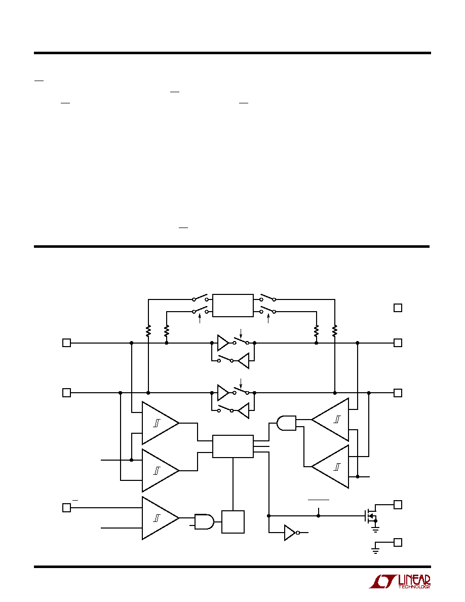
PI FU CTIO S
CS (Pin 1): The connection sense pin is a 1.4V threshold
digital input pin. For normal operation CS is grounded.
Driving CS above the 1.4V threshold isolates SDAIN from
SDAOUT and SCLIN from SCLOUT and asserts READY
low.
SCLOUT (Pin 2): Serial Clock Output. Connect this pin to
the SCL bus on the card.
SCLIN (Pin 3): Serial Clock Input. Connect this pin to SCL
on the bus backplane.
GND (Pin 4): Ground. Connect this pin to a ground plane
for best results.
READY (Pin 5): The READY pin is an open drain N-channel
MOSFET output which pulls down when CS is high or
when the start-up sequence described in the Operation
section has not been completed. READY goes high when
CS is low and a start-up is complete.
SDAIN (Pin 6): Serial Data Input. Connect this pin to the
SDA bus on the backplane.
SDAOUT (Pin 7): Serial Data Output. Connect this pin to
the SDA bus on the card.
V
CC
(Pin 8): Main Input Supply. Place a bypass capacitor
of at least 0.01
µ
F close to V
CC
for best results.
Exposed Pad (Pin 9): Exposed pad may be left open or
connected to device ground.
BLOCK DIAGRA
W
CONNECT PRECHARGE
CONNECT
PRECHARGE
CONNECT
CONNECT
1
R2
200k
R1
200k
R3
200k
R4
200k
PRECHARGE
LOGIC
PRECHARGE
CONNECT
95
µ
s
DELAY
UVLO
1.4V
CS
1.8V
3
SCLIN
6
SDAIN
1.8V
CONNECT
CONNECT
7
SDAOUT
8
V
CC
2
SCLOUT
READY
5
GND
4301 BD
4
LTC4301 Supply Independent 2-Wire Bus Buffer
5
LTC4301
4301fa
OPERATIO
U
Start-Up
When the LTC4301 first receives power on its V
CC
pin,
either during power-up or live insertion, it starts in an
undervoltage lockout (UVLO) state, ignoring any activity
on the SDA or SCL pins until V
CC
rises above 2.5V (typical).
This is to ensure that the part does not try to function until
it has enough voltage to do so.
During this time, the 1V precharge circuitry is active and
forces 1V through 200k nominal resistors to the SDA and
SCL pins. Because the I/O card is being plugged into a live
backplane, the voltage on the backplane SDA and SCL
busses may be anywhere between 0V and V
CC
. Precharging
the SCL and SDA pins to 1V minimizes the worst-case
voltage differential these pins will see at the moment of
connection, therefore minimizing the amount of distur-
bance caused by the I/O card.
Once the LTC4301 comes out of UVLO, it assumes that
SDAIN and SCLIN have been inserted into a live system
and that SDAOUT and SCLOUT are being powered up at
the same time as itself. Therefore, it looks for either a stop
bit or bus idle condition on the backplane side to indicate
the completion of a data transaction. When either one
occurs, the part also verifies that both the SDAOUT and
SCLOUT voltages are high. When all of these conditions
are met, the input-to-output connection circuitry is acti-
vated, joining the SDA and SCL busses on the I/O card with
those on the backplane.
Connection Circuitry
Once the connection circuitry is activated, the functional-
ity of the SDAIN and SDAOUT pins is identical. A low
forced on either pin at any time results in both pin voltages
being low. For proper operation, logic low input voltages
should be no higher than 0.4V with respect to the ground
pin voltage of the LTC4301. SDAIN and SDAOUT enter a
logic high state only when all devices on both SDAIN and
SDAOUT release high. The same is true for SCLIN and
SCLOUT. This important feature ensures that clock stretch-
ing, clock synchronization, arbitration and the acknowl-
edge protocol always work, regardless of how the devices
in the system are tied to the LTC4301.
Another key feature of the connection circuitry is that it
provides bidirectional buffering, keeping the backplane
and card capacitances isolated. Because of this isolation,
the waveforms on the backplane busses look slightly
different than the corresponding card bus waveforms as
described here.
Input-to-Output Offset Voltage
When a logic low voltage, V
LOW1
, is driven on any of the
LTC4301's data or clock pins, the LTC4301 regulates the
voltage on the other side of the device (call it V
LOW2
) at a
slightly higher voltage, as directed by the following
equation:
V
LOW2
= V
LOW1
+ 75mV + (V
CC
/R) ∑ 70
(typical)
where R is the bus pull-up resistance in ohms. For ex-
ample, if a device is forcing SDAOUT to 10mV where V
CC
= 3.3V and the pull-up resistor R on SDAIN is 10k, then the
voltage on SDAIN = 10mV + 75mV + (3.3/10000) ∑ 70 =
108mV (typical). See the Typical Performance Character-
istics section for curves showing the offset voltage as a
function of V
CC
and R.
Propagation Delays
During a rising edge, the rise time on each side is deter-
mined by the bus pull-up resistor and the equivalent
capacitance on the line. If the pull-up resistors are the
same, a difference in rise time occurs which is directly
proportional to the difference in capacitance between
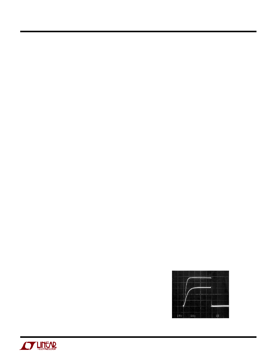
the two sides. This effect is displayed in Figure 1 for
V
CC
= 5V and a 10k pull-up resistor on each side (55pF on
one side and 20pF on the other). SDAIN and SCLIN are
pulled-up to 3.3V, and SDAOUT and SCLOUT are pulled-
up to 5V. Since the output side has less capacitance than
the input, it rises faster and the effective low to high
propagation delay is negative.
Figure 1. Input-Output Connection
4301 F01
OUTPUT
SIDE
20pF
INPUT
SIDE
55pF
1
µ
s/DIV
1V/DIV