Äîêóìåíòàöèÿ è îïèñàíèÿ www.docs.chipfind.ru
1
LTC4410
sn4410 4410fs
USB Power Manager
in ThinSOT
Manages Total Power Between a USB Peripheral
and Battery Charger
Minimal Voltage Drop (100mV at 500mA)
Ultralow Battery Drain: 1µA
Reverse Current Blocking Diode Not Required
Undervoltage Lockout
Very Few External Components
Compatible with Several LTC Linear Battery Chargers
Overtemperature Protected
Dual Battery Charge Priority Management
Low Profile (1mm) SOT-23 Package
Cellular Phones
PDAs
Digital Cameras
MP3 Players
Battery Backup Systems
, LTC and LT are registered trademarks of Linear Technology Corporation.
The LTC
®
4410 enables simultaneous battery charging and
operation of portable USB 1.0 and 2.0 compliant devices
while they are connected to a USB port. As the USB periph-
eral load increases, the LTC4410 proportionally reduces
the battery charge current to keep the total current less
than 500mA or 100mA, depending on the state of the MODE
pin.
The LTC4410 includes a USB present output that drives an
external P-channel MOSFET to disconnect the battery from
the USB peripheral when the USB power is valid. This
allows device operation when connected to the USB port,
even when the battery is deeply discharged.
Other features include reverse current blocking, thermal
shutdown and low quiescent current (80µA in 500mA
MODE) that is compliant with USB Suspend Mode.
The LTC4410 is available in the low profile (1mm) SOT-23
(ThinSOT
TM
) package.
ThinSOT is a trademark of Linear Technology Corporation.
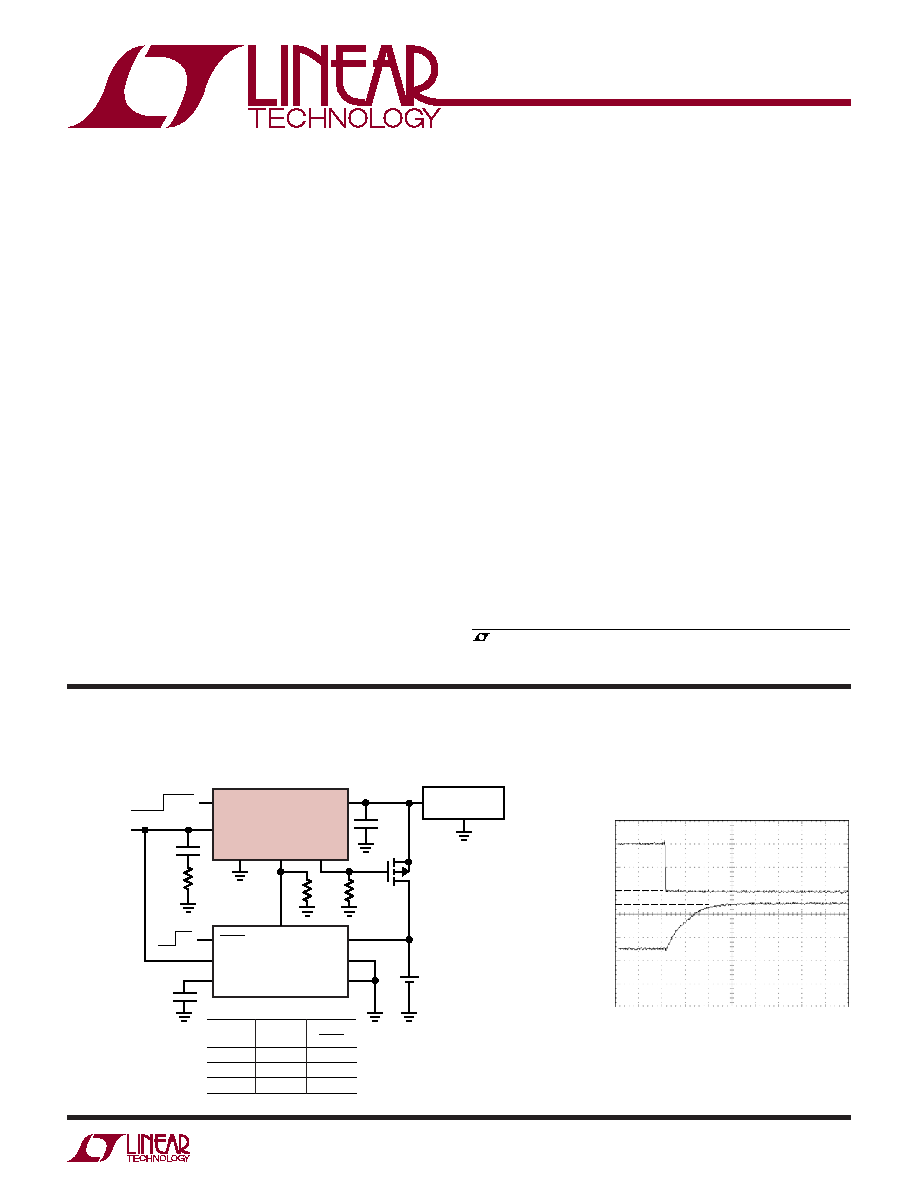
System Load Step Response
USB Powered Battery Charger and Power Manager
200mA
240mA
440mA
0mA
0mA
5µs/DIV
LOAD
CURRENT
BATTERY
CHARGER
CURRENT
4410 TA02
4.7µF
4.7µF
0.1µF
1
3.4k
1%
1M
V
OUT
GND
NTC
TIMER
1-CELL
Li-Ion
LTC4410
LTC4053
V
IN
V
CC
BAT
GND
SHDN
USBP
CHP
MODE
OFF ON
SYSTEM POWER
SUPPLY
USB
MODE
500mA
100mA
SUSPEND
LTC4410
MODE
1
0
1
LTC4053
SHDN
1
1
0
4.35V TO 5.5V
FROM
USB
100mA 500mA
4410 TA01
IRLML6401
PROG
FEATURES
DESCRIPTIO
U
APPLICATIO S
U
TYPICAL APPLICATIO
U
2
LTC4410
sn4410 4410fs
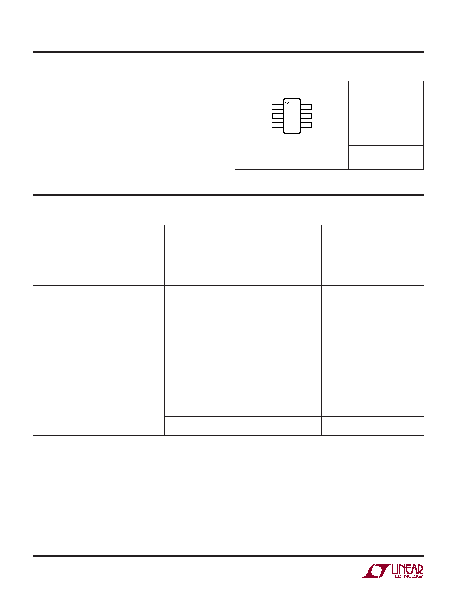
PARAMETER
CONDITIONS
MIN
TYP
MAX
UNITS
Operating V
IN
Range
4.35
5.5
V
Quiescent Current--Active
100mA Mode (MODE = Low)
500
700
µA
500mA Mode (MODE = High)
80
125
µA
CHP Compliance Voltage
MODE = 5V, I
VOUT
= 500mA
0
4.0
V
MODE = 0V, I
VOUT
= 0mA
0
3.5
V
Reverse Current
V
OUT
= 4V, V
IN
= 0V
1
5
µA
MODE Input Current
MODE = 0V
0.1
5
µA
MODE = 5V
0.1
5
µA
MODE Input High
1.2
V
MODE Input Low
0.4
V
USBP Output High
1M Resistor to GND, V
IN
= 5V
4.8
4.98
V
USBP Output Low
1M Resistor to V
IN
, V
IN
= 3.5V
20
100
mV
UVLO and USBP Threshold
Measured on V
IN
Rising
4.05
4.2
4.35
V
UVLO and USBP Hysteresis
Measured on V
IN
80
100
120
mV
CHP Output Current
MODE = High, I
VOUT
= 0mA (Note 2)
0
30
µA
MODE = High, I
VOUT
= 500mA (Note 2)
470
500
530
µA
MODE = High, I
VOUT
= 500mA, T
A
0°C, (Note 2)
460
500
540
µA
MODE = High, I
VOUT
= 500mA, T
A
< 0°C, (Note 2)
450
500
550
µA
MODE = Low, I
VOUT
= 0mA (Note 2)
370
µA
MODE = Low, I
VOUT
= 100mA (Note 2)
430
470
510
µA
(Note 1)
V
IN
, V
OUT
Voltages ...................................... 0.3V to 6V
USBP, MODE, CHP Voltage ........................ 0.3V to 6V
I
VOUT
(Note 5) ............................................................ 2A
Operating Ambient Temperature Range
LTC4410E (Notes 3, 4) ........................40°C to 85°C
Storage Temperature Range ................. 65°C to 150°C
Lead Temperature (Soldering, 10 sec).................. 300°C
ABSOLUTE
M
AXI
M
U
M
RATINGS
W
W
W
U
PACKAGE/ORDER I
N
FOR
M
ATIO
N
W
U
U
ORDER PART
NUMBER
LTC4410ES6
S6 PART MARKING
LTK8
T
JMAX
= 125°C,
JA
= 100°C/W TO 150°C/W
DEPENDING ON PC BOARD LAYOUT
The
denotes specifications that apply over the full operating temperature
range, otherwise specifications are at T
A
= 25°C. V
IN
= 5V unless otherwise noted.
Consult LTC Marketing for parts specified with wider operating temperature ranges.
V
IN
1
GND 2
MODE 3
6 V
OUT
5 CHP
4 USBP
TOP VIEW
S6 PACKAGE
6-LEAD PLASTIC TSOT-23
ELECTRICAL CHARACTERISTICS
Note 1: Absolute Maximum Ratings are those values beyond which the life
of a device may be impaired.
Note 2: Current flows out of CHP, voltage at CHP = 0V.
Note 3: The LTC4410E is guaranteed to meet performance specifications
from 0°C to 70°C. Specifications over the 40°C to 85°C operating
temperature range are assured by design, characterization and correlation
with statistical process controls.
Note 4: This IC includes overtemperature protection that is intended to
protect the device during momentary overload conditions. Junction
temperature will exceed 125°C when overtemperature protection is active.
Continuous operation above the specified maximum operating junction
temperature may impair device reliability.
Note 5: Based on long-term current density limitations.
3
LTC4410
sn4410 4410fs
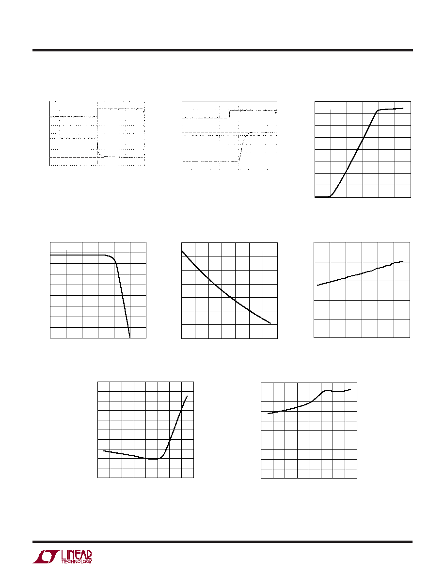
TYPICAL PERFOR A CE CHARACTERISTICS
U
W
I
REF
Turn-Off Response
V
IN
(V)
0
I
REF
(
µ
A)
150
200
250
3
5
4410 G03
100
50
0
1
2
4
300
350
400
6
T
A
= 25°C
MODE PIN
CHP CURRENT
INTO A 3.4k
RESISTOR
0mA
0V
5V
1µs/DIV
4410 G01
370µA
CHP CURRENT
INTO A 3.4k
RESISTOR
500mA LOAD STEP
0mA
10µs/DIV
4410 G02
500µA
0mA
500mA
CHP Current with I
LOAD
Step
I
REF
vs V
IN
(MODE = 0)
I
REF
vs V
CHP
(MODE = 0)
R
DS(ON)
vs V
IN
V
CHP
(V)
0
0
I
REF
(
µ
A)
50
150
200
250
2
450
4410 G04
100
1
6
3
4
5
300
350
400
T
A
= 25°C
V
IN
(V)
4.2
170
172
176
4.8
5.2
4410 G05
168
166
4.4
4.6
5.0
5.4
5.6
164
162
174
R
DS(ON)
(m
)
T
A
= 25°C
R
DS(ON)
vs Temperature
TEMPERATURE (°C)
50
0
R
DS(ON)
(m
)
50
100
150
200
250
25
0
25
50
4410 G06
75
100
Reverse Current vs Temperature
I
CC
vs Temperature
TEMPERATURE (°C)
60
0
REVERSE CURRENT (
µ
A)
0.5
1.5
2.0
2.5
5.0
3.5
20
20
40
4410 G07
1.0
4.0
4.5
3.0
40
0
60
80
100
TEMPERATURE (°C)
60
0
I
CC
(
µ
A)
10
30
40
50
100
70
20
20
40
4410 G08
20
80
90
60
40
0
60
80
100
4
LTC4410
sn4410 4410fs
V
IN
(Pin 1): Positive Input Supply. When V
IN
> 4.2V, the
internal undervoltage lockout enables the main switch that
connects V
IN
to V
OUT
. Bypass V
IN
with a 10µF ceramic
capacitor and a 1 resistor in series or use a 10µF
capacitor with at least 1 minimum ESR. This minimizes
the voltage transient that can occur when the input is hot
switched.
GND (Pin 2): Signal Ground for the LTC4410.
MODE (Pin 3): Mode Select Input. This pin selects the
maximum USB port current of either 100mA or 500mA.
When MODE is high, the current out of CHP will be I
VOUT
/
1000. When MODE is low, the current out of CHP will be
I
VOUT
/1000 + 370µA (typical).
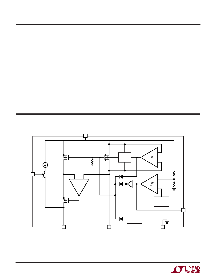
BLOCK DIAGRA
W
THERMAL
SHUTDOWN
M2
×1000
VB
USBP
M1
×1
M3
370µA
S1
MODE
CHP
R1
+
REF
1.25V
R3
R2
V
IN
1
3
5
V
OUT
6
GND
4410 BD
USBP
2
4
+
BODY
SWITCH
+
U
U
U
PI FU CTIO S
USBP (Pin 4): USB Voltage Present Output. This pin goes
high when V
IN
exceeds the undervoltage lockout threshold
(4.2V typical).
CHP (Pin 5): Charger Program Output. This pin sources a
current that is used by the battery charger to control
charge current.
V
OUT
(Pin 6): LTC4410 Output. Bypass this pin with a
10µF or larger X5R ceramic capacitor. This capacitor
may be omitted if other circuitry connected to V
OUT
contains a bypass capacitor. When V
OUT
> V
IN
, the internal
switch is held off, resulting in very low battery drain
current (1µA typical).

5
LTC4410
sn4410 4410fs
OPERATIO
U
The LTC4410 manages the total current consumption
between a battery charger and a USB portable device. In
a system using the LTC4410, a battery charger can be set
up to charge at the maximum available current from the
USB port without any need to reserve current for the
device load. As the USB device current increases, the
LTC4410 decreases the battery charge current so as not
to exceed the maximum allowable current from the USB
port. This allows for simultaneous battery charging and
device operation. The LTC4410 can only reduce the bat-
tery charge current to zero. It is the responsibility of the
USB device load to not exceed the USB power limits.
The LTC4410 uses an internal power MOSFET to sense
load current. This MOSFET is held off when V
OUT
> V
IN
or
V
IN
< 4.2V (typ). A replica of the I
VOUT
current equal to
I
VOUT
/1000 is sourced out of the CHP pin with an accuracy
of ±6%. This current can be summed into the PROG node
of a battery charger to reduce the charge current. The
LTC4410 is primarily designed to interface with battery
chargers that use a program pin to set the maximum
charge current, with a charge current to program pin
current ratio of 1000:1. The voltage on CHP can be
externally monitored to signal overcurrent conditions.
When V
IN
> 4.2V, the internal USB present comparator
forces the USBP pin high. This signal can be used to detect
when the USB voltage is present and drive an external
switch to connect or disconnect a battery from the USB
peripheral.
The MODE pin controls the state of an internal 370µA
current reference (I
REF
). When active (MODE pin low), the
total current sourced out of CHP is I
VOUT
/1000 +I
REF
. The
primary function of the current reference is to offset the
battery charger charge current for 100mA mode. When
MODE is high, the current reference is disabled. The total
current out of CHP with MODE high is I
VOUT
/1000. The
MODE controlled current offset makes it possible to con-
figure the battery charger and the LTC4410 to support the
USB specification 1.0 and 2.0 required 100mA and 500mA
modes of operation.
The low quiescent current (80µA, when MODE is high) of
the LTC4410 makes the system easily compliant with the
USB specifications 1.0 and 2.0 SUSPEND MODE current
consumption requirements.
When V
OUT
> V
IN
, the LTC4410 transitions to low power
mode, draining 1µA (typical) from the Lithium-Ion battery.
This condition occurs when the USB device is operating
off of its internal battery and not connected to the USB
port.