Äîêóìåíòàöèÿ è îïèñàíèÿ www.docs.chipfind.ru
1
LTC4557
4557f
s
GSM and 3G Cellular Phones
s
Wireless P.O.S. Terminals
s
Multiple SAM Card Interface
s
Power Management and Signal Level Translators
for Two SIM Cards or Smart Cards
s
Independent 1.8V/3V V
CC
Control for Both Cards
s
Automatic Level Translation
s
ISO7816, ETSI and EMV Compatible
s
Dynamic Pull-Ups Deliver Fast Signal Rise Times*
s
Built-In Fault Protection Circuitry
s
Automatic Activation/Deactivation Sequencing
Circuitry
s
Low Operating/Shutdown Current
s
>10kV ESD on SIM Card Pins
s
Compatible with EMV Fault Tolerance Requirements
s
Available in 16-Lead (3mm
×
3mm) QFN Package
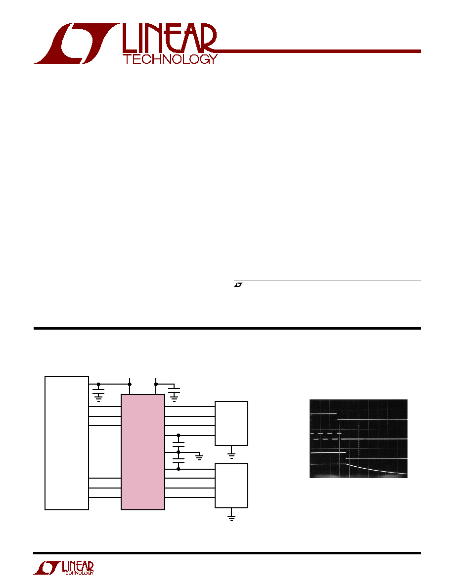
Dual SIM/Smart Card
Power Supply and Interface
Deactivation Sequence
, LTC and LT are registered trademarks of Linear Technology Corporation.
The LTC
®
4557 provides power conversion and signal level
translation needed for 2.5G and 3G cellular telephones to
interface with 1.8V or 3V subscriber identity modules
(SIMs). The part meets all requirements for 1.8V and 3V
SIMs. The part contains LDO regulators to power 1.8V or
3V SIM cards from a 2.7V to 5.5V input. The output
voltages can be set using the two voltage selection pins
and up to 50mA of load current can be supplied.
Internal level translators allow controllers operating with
supplies as low as 1.2V to interface with 1.8V or 3V smart
cards. Battery life is maximized by a low operating current
of less than 100
µ
A and a shutdown current of less than
1
µ
A. Board area is minimized by the low profile 3mm
×
3mm
×
0.75mm leadless QFN package.
DV
CC
V
BATT
V
BATT
3V TO 6V
DV
CC
1.2V TO 4.4V
LTC4557
µ
CONTROLLER
V
CCA
I/OA
DV
CC
RSTA
CLKA
C1
C1
C5
C5
C3
C2
C7
C7
C2
C3
GND
V
CCB
CLKB
RSTB
I/OB
CLKIN
0.1
µ
F
1
µ
F
1
µ
F
RSTIN
DATA
ENABLE
M0
M1
0.1
µ
F
4557 TA01
1.8V/3V
SIM
CARD
1.8V/3V
SMART
CARD
V
CC
I/O
RST
CLK
GND
GND
V
CC
CLK
RST
I/O
*U.S. Patent No. 6,356,140
RSTX
5V/DIV
CLKX
5V/DIV
I/OX
5V/DIV
V
CCX
2V/DIV
10
µ
s/DIV
C
VCCX
= 1
µ
F
4557 G07
FEATURES
DESCRIPTIO
U
APPLICATIO S
U
TYPICAL APPLICATIO
U
2
LTC4557
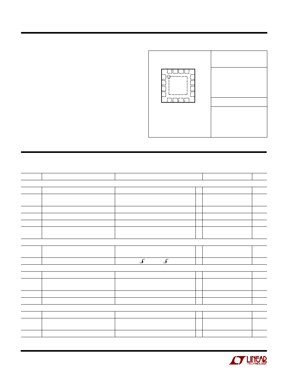
4557f
T
JMAX
= 125
°
C,
JA
= 68
°
C/W,
JC
= 42
°
C/W
EXPOSED PAD (PIN 17) IS GND
(MUST BE SOLDERED TO PCB)
16 15 14 13
5
6
7
8
TOP VIEW
17
UD PACKAGE
16-LEAD (3mm
×
3mm) PLASTIC QFN
9
10
11
12
4
3
2
1
V
CCB
DV
CC
V
BATT
V
CCA
CLKA
RSTA
I/OA
DATA
M0
M1
CLKIN
RSTIN
CLKB
RSTB
I/OB
ENABLE
V
BATT
, DV
CC
, DATA, RSTIN, CLKIN,
ENABLE, M0, M1 to GND ............................ 0.3V to 6V
I/OA, CLKA, RSTA ........................ 0.3V to V
CCA
+ 0.3V
I/OB, CLKB, RSTB ........................ 0.3V to V
CCB
+ 0.3V
I
CCA,B
(Note 4) ...................................................... 80mA
V
CCA,B
Short-Circuit Duration ......................... Indefinite
Operating Temperature Range (Note 3) .. 40
°
C to 85
°
C
Storage Temperature Range ................... 65
°
C to 125
°
ORDER PART
NUMBER
UD PART MARKING
LAHP
LTC4557EUD
(Note 1)
The
q
denotes the specifications which apply over the full operating
temperature range, otherwise specifications are at T
A
= 25
°
C. V
BATT
= 3.3V, DV
CC
= 1.8V, unless otherwise specified.
ABSOLUTE AXI U RATI GS
W
W
W
U
PACKAGE/ORDER I FOR ATIO
U
U
W
ELECTRICAL CHARACTERISTICS
Consult LTC Marketing for parts specified with wider operating temperature ranges.
SYMBOL
PARAMETER
CONDITIONS
MIN
TYP
MAX
UNITS
Input Power Supply
V
BATT
Operating Voltage
q
2.7
5.5
V
I
VBATT
Operating Current
V
CCA
= 3V, V
CCB
= 0V, I
CCA
= I
CCB
= 0
µ
A
q
65
100
µ
A
V
CCA
= 1.8V, V
CCB
= 0V, I
CCA
= I
CCB
= 0
µ
A
q
65
100
µ
A
DV
CC
Operating Voltage
q
1.2
5.5
V
I
DVCC
Operating Current
q
6
10
µ
A
I
DVCC
Shutdown Current
q
0.1
1
µ
A
I
VBATT
Shutdown Current
q
0.4
2.5
µ
A
DV
CC
= 0V
q
0.1
1.0
µ
A
SIM Card Supplies
V
CCA,B
Output Voltage
3V Mode, 0mA < I
CCA,B
< 50mA
q
2.75
3.0
3.25
V
1.8V Mode, 0mA < I
CCA,B
< 3OmA
q
1.65
1.8
1.95
V
Channel Turn-On Time
I
CCA,B
= 0mA,
ENABLE to
I
OA/B
q
1.3
2.5
ms
CLKA, CLKB
V
OL
Low Level Output Voltage
Sink Current = 200
µ
A (Note 2)
q
0.2
V
V
OH
High Level Output Voltage
Source Current = 200
µ
A (Note 2)
q
V
CCA,B
V
0.2
Rise, Fall Time
Loaded with 33pF (10% to 90%) (Note 2)
q
16
ns
CLKA, CLKB Frequency
(Note 2)
q
10
MHz
RSTA, RSTB
V
OL
Low Level Output Voltage
Sink Current = 200
µ
A (Note 2)
q
0.2
V
V
OH
High Level Output Voltage
Source Current = 200
µ
A (Note 2)
q
V
CCA,B
V
0.2
Rise, Fall Time
Loaded with 33pF (10% to 90%) (Note 2)
q
100
ns
3
LTC4557
4557f
The
q
denotes the specifications which apply over the full operating
temperature range, otherwise specifications are at T
A
= 25
°
C. V
BATT
= 3.3V, DV
CC
= 1.8V, unless otherwise specified.
ELECTRICAL CHARACTERISTICS
SYMBOL
PARAMETER
CONDITIONS
MIN
TYP
MAX
UNITS
I/OA, I/OB
V
OL
Low Level Output Voltage
Sink Current = 1mA (V
DATA
= 0V) (Note 2)
q
0.3
V
V
OH
High Level Output Voltage
Source Current = 20
µ
A (V
DATA
= V
DVCC
)
q
0.85 ·
V
(Note 2)
V
CCA,B
Rise Time
Loaded with 33pF (10% to 90%) (Note 2)
q
200
500
ns
Short-Circuit Current
V
DATA
= 0V (Note 2)
q
5
10
mA
DATA
V
OL
Low Level Output Voltage
Sink Current = 500
µ
A (V
I/OA,B
= 0V)
q
0.3
V
V
OH
High Level Output Voltage
Source Current = 20
µ
A (V
I/OA,B
= V
CCA,B
)
q
0.8 ·
V
DV
CC
Rise Time
Loaded with 33pF (10% to 90%)
q
200
500
ns
RSTIN, CLKIN, ENABLE, M0, M1
V
IL
Low Input Threshold
q
0.15 ·
V
DV
CC
V
IH
High Input Threshold
q
0.85 ·
V
DV
CC
Input Current (I
IH
, I
IL
)
q
1
1
µ
A
Note 1: Absolute Maximum Ratings are those values beyond which the life
of a device may be impaired.
Note 2: This specification applies to both 1.8V and 3V smart cards.
Note 3: The LTC4557E is guaranteed to meet performance specifications
from 0
°
C to 70
°
C. Specifications over the 40
°
C to 85
°
C operating
temperature range are assured by design, characterization and correlation
with statistical process controls.
Note 4: Based on long term current density limitations.
4
LTC4557
4557f
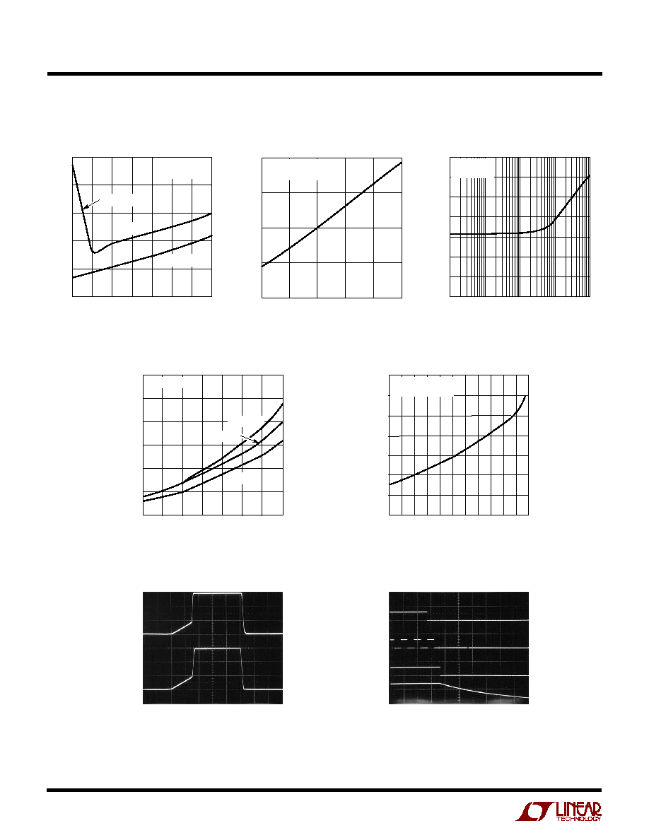
TYPICAL PERFOR A CE CHARACTERISTICS
U
W
I/O X Short-Circuit Current
vs Temperature
No Load Supply Current vs V
BATT
V
BATT
Quiescent Current
(I
VBATT
I
CC
) vs Load Current
V
BATT
Shutdown Current
vs Supply Voltage
DV
CC
Shutdown Current
vs Supply Voltage
Data I/O Channel, C
L
= 40pF
Deactivation Sequence,
C
VCCX
= 1
µ
F
SUPPLY VOLTAGE (V)
2.7
3.1
55
SUPPLY CURRENT (
µ
A)
65
80
3.5
4.3
4.7
4557 G01
60
75
70
3.9
5.1
5.5
T
A
= 25
°
C
I
CCA
= I
CCB
= 0
µ
A
V
CCX
= 3V
V
CCX
= 1.8V
DROPOUT
TEMPERATURE (
°
C)
40
SHORT-CIRCUIT CURRENT (mA)
5.0
5.5
60
4557 G02
4.5
4.0
15
10
35
85
6.0
V
DVCC
= V
BATT
= 5.5V
V
CCX
= 3V
LOAD CURRENT (
µ
A)
40
SUPPLY CURRENT (
µ
A)
80
120
140
10
1000
10000
100000
4557 G03
0
100
100
60
20
T
A
= 25
°
C
V
BATT
= 3.1V
SUPPLY VOLTAGE (V)
2.7
SUPPLY CURRENT (
µ
A)
2.0
2.5
3.0
3.9
4.7
4557 G04
1.5
1.0
3.1
3.5
4.3
5.1
5.5
0.5
0
V
DVCC
= 1.8V
T
A
= 40
°
C
T
A
= 25
°
C
T
A
= 85
°
C
SUPPLY VOLTAGE (V)
1.2
0
SUPPLY CURRENT (
µ
A)
0.1
0.3
0.4
0.5
0.7
1.6
3.2
4
4557 G05
0.2
0.6
2.8
4.8
5.6
5.2
2 2.4
3.6
4.4
V
BATT
= 5.5V
T
A
= 40
°
C TO 85
°
C
I/0X
1V/DIV
DATA
1V/DIV
200ns/DIV
C
L
= 40pF
4557 G06
RSTX
5V/DIV
CLKX
5V/DIV
I/OX
5V/DIV
V
CCX
2V/DIV
10
µ
s/DIV
C
VCCX
= 1
µ
F
4557 G07
5
LTC4557
4557f
DATA (Pin 8): Input/Output. Microcontroller side data I/O
pin. The DATA pin provides the bidirectional communica-
tion path to both cards. Only one of the cards may be
selected to communicate via the DATA pin. The pin pos-
sesses a dynamically activated pull-up current source,
allowing the controller to use an open-drain output. The
current source maintains a HIGH state. This pin is held
HIGH by a weak pull-up when the ENABLE pin is LOW.
RSTIN (Pin 9): Input. The RSTIN pin supplies the reset
signal to the cards. It is level shifted and transmitted
directly to the RST pin of the selected card.
CLKIN (Pin 10): Input. The CLKIN pin supplies the clock
signal to the cards. It is level shifted and transmitted
directly to the CLK pin of the selected card.
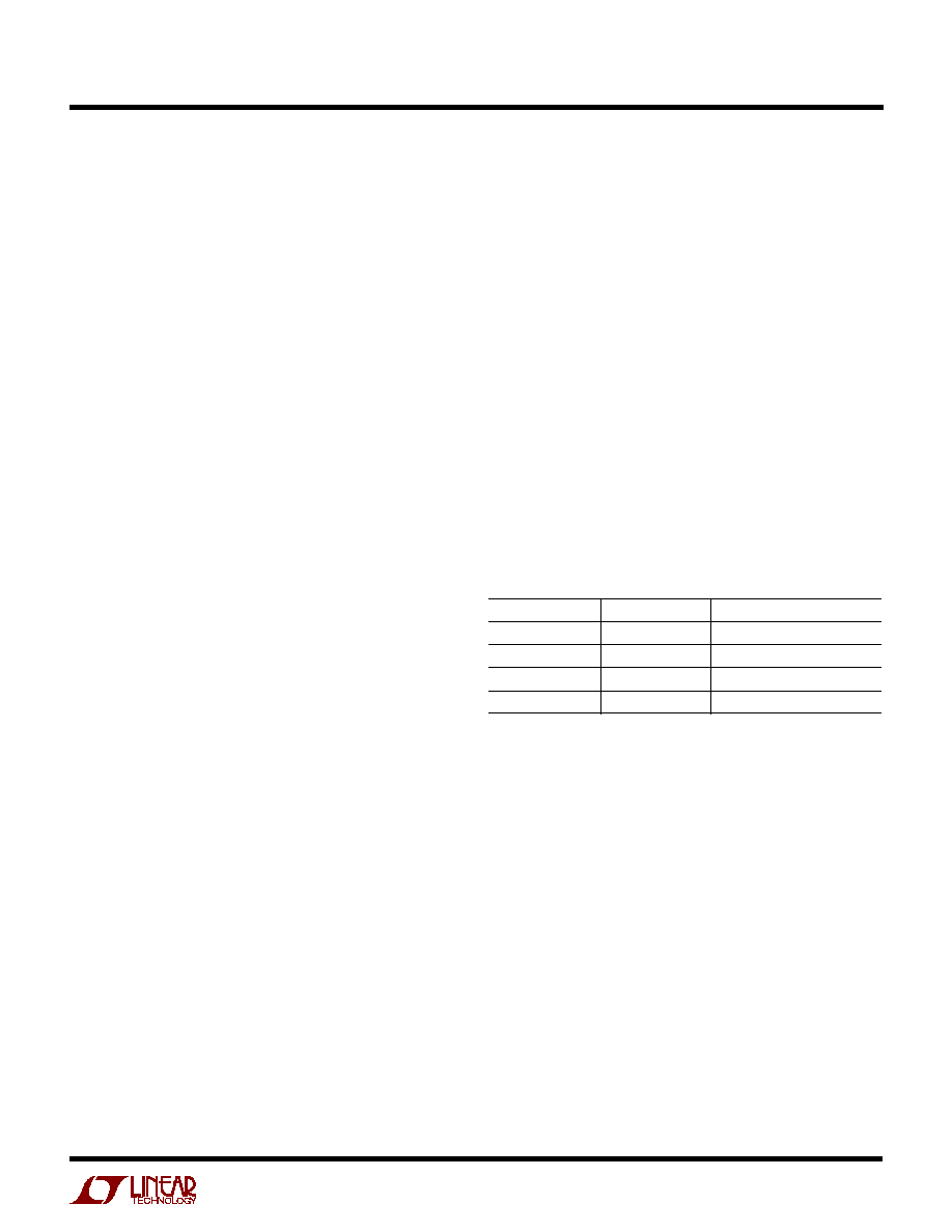
M0/M1 (Pins 12, 11): Inputs. The M0 and M1 pins select
which set of SIM/smart card pins are active and at which
voltage level they operate. The truth table for these pins
follows:
M1
M0
SELECTED CARD/VOLTAGE
0
0
Card A/1.8V
0
1
Card A/3V
1
0
Card B/1.8V
1
1
Card B/3V
ENABLE (Pin 13): Input. The ENABLE pin shuts down the
chip when LOW.
EXPOSED PAD (Pin 17): Chip Ground. This ground pad
must be soldered directly to a PCB ground plane.
U
U
U
PI FU CTIO S
DV
CC
(Pin 2): Power. Reference voltage for the control
logic.
V
BATT
(Pin 3): Power. Supply voltage for the analog
sections of the LTC4557.
V
CCA
/V
CCB
(Pins 4, 1): Card Socket. The V
CCA
/V
CCB
pins
should be connected to the V
CC
pins of the respective card
sockets. The activation of the V
CCA
/V
CCB
pins is controlled
by the M0, M1 and ENABLE inputs. They can be set to 0V,
1.8V or 3V. Only one of the two, either V
CCA
or V
CCB
, may
be active at a time.
CLKA/CLKB (Pins 5, 16): Card Socket. The CLKA/CLKB
pins should be connected to the CLK pins of the respective
card sockets. The CLKA/CLKB signals are derived from the
CLKIN pin. They provide a level shifted CLKIN signal to the
selected card. The CLKA/CLKB pins are gated off until
V
CCA
/V
CCB
attain their correct values.
RSTA/RSTB (Pins 6, 15): Card Socket. The RSTA/RSTB
pins should be connected to the RST pins of the respective
card sockets. The RSTA/RSTB signals are derived from
the RSTIN pin. When a card is selected, its RST pin follows
RSTIN. The RSTA/RSTB pins are gated off until V
CCA
/V
CCB
attain their correct values.
I/OA, I/OB (Pins 7, 14): Card Socket. The I/OA, I/OB pins
connect to the I/O pins of the respective card sockets.
When a card is selected, its I/O pin transmits/receives data
to/from the DATA pin. The I/OA, I/OB pins are gated off
until V
CCA
/V
CCB
attain their correct values.