 | –≠–ª–µ–∫—Ç—Ä–æ–Ω–Ω—ã–π –∫–æ–º–ø–æ–Ω–µ–Ω—Ç: LTC486CS | –°–∫–∞—á–∞—Ç—å:  PDF PDF  ZIP ZIP |
1
LTC486
Quad Low Power
RS485 Driver
D
U
ESCRIPTIO
U
A
O
PPLICATI
TYPICAL
DATA RATE (bps)
10k
10
CABLE LENGTH (FT)
100
1k
10k
100k
1M
10M
LTC486 ∑ TA09
2.5M
* APPLIES FOR 24 GAUGE, POLYETHYLENE
DIELECTRIC TWISTED PAIR
RS485 Cable Length Specification*
s
Low Power RS485/RS422 Drivers
s
Level Translator
U
S
A
O
PPLICATI
S
FEATURE
s
Very Low Power: I
CC
= 110
µ
A Typ
s
Designed for RS485 or RS422 Applications
s
Single 5V Supply
s
≠ 7V to 12V Bus Common-Mode Range Permits
±
7V GND Difference Between Devices on the Bus
s
Thermal Shutdown Protection
s
Power-Up/Down Glitch-Free Driver Outputs Permit
Live Insertion/Removal of Package
s
Driver Maintains High Impedance in Three-State or
with the Power Off
s
28ns Typical Driver Propagation Delays
with 5ns Skew
s
Pin Compatible with the SN75172, DS96172,
µ
A96172, and DS96F172
The LTC486 is a low power differential bus/line driver
designed for multipoint data transmission standard RS485
applications with extended common-mode range (12V to
≠7V). It also meets RS422 requirements.
The CMOS design offers significant power savings over its
bipolar counterpart without sacrificing ruggedness against
overload or ESD damage.
The driver features three-state outputs, with the driver
outputs maintaining high impedance over the entire
common-mode range. Excessive power dissipation caused
by bus contention or faults is prevented by a thermal
shutdown circuit which forces the driver outputs into a
high impedance state.
Both AC and DC specifications are guaranteed from 0
∞
C to
70
∞
C (Commercial), ≠ 40
∞
C to 85
∞
C (Industrial), over the
4.75V to 5.25V supply voltage range.
LTC486 ∑ TA01
RECEIVER
EN
DI
EN
4
4
12
1
1/4 LTC486
120
120
RO
3
EN
2
1
1/4 LTC488
4000 FT BELDEN 9841
DRIVER
LTC486
2
A
U
G
W
A
W
U
W
A
R
BSOLUTE
XI
TI
S
W
U
U
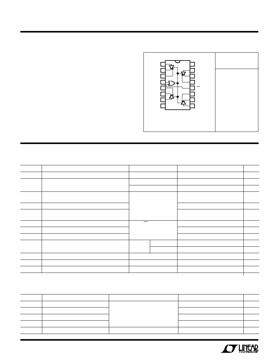
PACKAGE/ORDER I FOR ATIO
(Note 1)
Supply Voltage (V
CC
) ............................................... 12V
Control Input Voltages .................... ≠ 0.5V to V
CC
+ 0.5V
Driver Input Voltages ...................... ≠ 0.5V to V
CC
+ 0.5V
Driver Output Voltages .........................................
±
14V
Control Input Currents .......................................
±
25mA
Driver Input Currents .........................................
±
25mA
Operating Temperature Range
LTC486C ................................................ 0
∞
C to 70
∞
C
LTC486I ............................................ ≠ 40
∞
C to 85
∞
C
Storage Temperature Range ................. ≠ 65
∞
C to 150
∞
C
Lead Temperature (Soldering, 10 sec)................. 300
∞
C
ORDER PART
NUMBER
LTC486CN
LTC486CS
LTC486IN
LTC486IS
T
JMAX
= 125
∞
C,
JA
= 70
∞
C/W (N)
T
JMAX
= 150
∞
C,
JA
= 95
∞
C/W (S)
Consult factory for Military grade parts
16
15
14
13
12
11
10
9
8
7
6
5
4
3
2
1
DI1
DO1A
DO1B
EN
DO2B
DO2A
DI2
GND
DI3
DO3A
DO3B
EN
DO4B
DO4A
DI4
V
N PACKAGE
16-LEAD PLASTIC DIP
TOP VIEW
CC
S PACKAGE
16-LEAD PLASTIC SOL
V
CC
= 5V
±
5%, 0
∞
C
Temperature
70
∞
C (Commercial), ≠ 40
∞
C
Temperature
85
∞
C (Industrial) (Note 2, 3)
ELECTRICAL C
C
HARA TERISTICS
C
D
SYMBOL
PARAMETER
CONDITIONS
MIN
TYP
MAX
UNITS
t
PLH
Driver Input to Output
R
DIFF
= 54
,
C
L1
= C
L2
= 100pF
10
30
50
ns
t
PHL
Driver Input to Output
(Figures 2, 4)
10
30
50
ns
t
SKEW
Driver Output to Output
5
15
ns
t
r,
t
f
Driver Rise or Fall Time
5
15
25
ns
t
ZH
Driver Enable to Output High
C
L
= 100pF (Figures 3, 5) S2 Closed
35
70
ns
S
U
G C
C
HARA TERISTICS
WITCHI
V
CC
= 5V
±
5%, 0
∞
C
Temperature
70
∞
C (Commercial), ≠ 40
∞
C
Temperature
85
∞
C (Industrial) (Note 2, 3)
SYMBOL
PARAMETER
CONDITIONS
MIN
TYP
MAX
UNITS
V
OD1
Differential Driver Output Voltage (Unloaded)
I
O
= 0
5
V
V
OD2
Differential Driver Output Voltage (With Load)
R = 50
; (RS422)
2
V
R = 27
; (RS485) (Figure 1)
1.5
5
V
V
OD
Change in Magnitude of Driver Differential
R = 27
or R = 50
0.2
V
Output Voltage for Complementary Output States
(Figure 1)
V
OC
Driver Common-Mode Output Voltage
3
V
V
OC
Change in Magnitude of Driver Common-Mode
0.2
V
Output Voltage for Complementary Output States
V
IH
Input High Voltage
DI, EN, EN
2.0
V
V
IL
Input Low Voltage
0.8
V
I
IN1
Input Current
±
2
µ
A
I
CC
Supply Current
No Load Output Enabled
110
200
µ
A
Output Disabled
110
200
µ
A
I
OSD1
Driver Short-Circuit Current, V
OUT
= High
V
O
= ≠ 7V
100
250
mA
I
OSD2
Driver Short-Circuit Current, V
OUT
= Low
V
O
= 12V
100
250
mA
I
OZ
High Impedance State Output Current
V
O
= ≠ 7V to 12V
±
10
±
200
µ
A
3
LTC486
S
U
G C
C
HARA TERISTICS
WITCHI
SYMBOL
PARAMETER
CONDITIONS
MIN
TYP
MAX
UNITS
t
ZL
Driver Enable to Output Low
C
L
= 100pF (Figures 3, 5) S1 Closed
35
70
ns
t
LZ
Driver Disable Time from Low
C
L
= 15pF (Figures 3, 5) S1 Closed
35
70
ns
t
HZ
Driver Disable Time from High
C
L
= 15pF (Figures 3, 5) S2 Closed
35
70
ns
Note 1: Absolute maximum ratings are those beyond which the safety of
the device cannot be guaranteed.
Note 2: All currents into device pins are positive; all currents out of device
pins are negative. All voltages are referenced to device ground unless
otherwise specified.
Note 3: All typicals are given for V
CC
= 5V and temperature = 25
∞
C.
TI
W
E WAVEFOR
S
U
G
WITCHI
W
S
V
CC
= 5V
±
5%, 0
∞
C
Temperature
70
∞
C (Commercial), ≠ 40
∞
C
Temperature
85
∞
C (Industrial) (Note 2, 3)
OUTPUT VOLTAGE (V)
0
OUTPUT CURRENT (mA)
0
≠24
≠ 48
≠72
≠96
1
2
3
4
LTC486 ∑ TPC01
OUTPUT VOLTAGE (V)
0
OUTPUT CURRENT (mA)
0
20
40
60
80
1
2
3
4
LTC486 ∑ TPC03
OUTPUT VOLTAGE (V)
0
OUTPUT CURRENT (mA)
0
16
32
48
64
1
2
3
4
LTC486∑ TPC02
Figure 4. Driver Propagation Delays
C
C
HARA TERISTICS
U
W
A
TYPICAL PERFOR
CE
Driver Output High Voltage
Driver Differential Output Voltage
Driver Output Low Voltage
vs Output Current T
A
= 25
∞
C
vs Output Current T
A
= 25
∞
C
vs Output Current T
A
= 25
∞
C
≠V
O
LTC486 ∑ TA05
B
A
DI
V
O
1/2 V
O
3V
0V
t
SKEW
1.5V
t
PLH
1.5V
t
PHL
1/2 V
O
V = V(A) ≠ V(B)
V
O
80%
20%
t
f
90%
DIFF
10%
t
SKEW
t
r
f = 1MHz : t 10ns : t 10ns
<
<
r
f
LTC486 ∑ TA06
A, B
EN
3V
0V
f = 1MHz : t 10ns : t 10ns
V
OL
V
OH
1.5V
1.5V
5V
OUTPUT NORMALLY LOW
t
ZL
2.3V
t
LZ
0.5V
A, B
0V
t
ZH
2.3V
OUTPUT NORMALLY HIGH
t
HZ
0.5V
r
f
Figure 5. Driver Enable and Disable Times
LTC486
4
C
C
HARA TERISTICS
U
W
A
TYPICAL PERFOR
CE
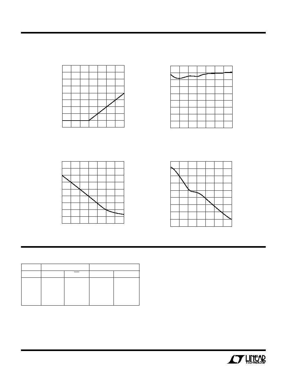
TTL Input Threshold vs Temperature
TEMPERATURE (
∞
C )
≠50
INPUT THRESHOLD VOLTAGE (V)
1.55
1.57
1.59
1.61
1.63
0
50
100
LTC486 ∑ TPC04
Driver Skew vs Temperature
Driver Differential Output Voltage
vs Temperature R
O
= 54
TEMPERATURE (
∞
C )
≠50
SUPPLY CURRENT (
µ
A)
90
100
110
120
130
0
50
100
LTC486 ∑ TPC06
Supply Current vs Temperature
INPUT
ENABLES
OUTPUTS
DI
EN
EN
OUTA
OUTB
H
H
X
H
L
L
H
X
L
H
H
X
L
H
L
L
X
L
L
H
X
L
H
Z
Z
FU
U
C
UO
TI
TABLE
H: High Level
L: Low Level
X: Irrelevant
Z: High Impedance (Off)
TEMPERATURE (
∞
C )
≠50
DIFFERENTIAL VOLTAGE (V)
1.5
1.7
1.9
2.1
2.3
0
50
100
LTC486 ∑ TPC07
TEMPERATURE (
∞
C )
≠50
TIME (ns)
1
2
3
4
5
0
50
100
LTC486 ∑ TPC05

5
LTC486
Figure 1. Driver DC Test Load
Figure 3. Driver Timing Test Load #2
Figure 2. Driver Timing Test Circuit
DRIVER
LTC486 ∑ TA03
EN
DI
A
B
EN
R
DIFF
CI1
CI2
TEST CIRCUITS
GND (Pin 8): Ground Connection.
DI3 (Pin 9): Driver 3 Input. Refer to DI1.
DO3A (Pin 10): Driver 3 Output.
DO3B (Pin 11): Driver 3 Output.
EN (Pin 12): Driver Outputs Disabled. See Function Table
for details.
DO4B (Pin 13): Driver 4 Output.
DO4A (Pin 14): Driver 4 Output.
DI4 (Pin 15): Driver 4 Input. Refer to DI1.
V
CC
(Pin 16): Positive Supply; 4.75V < V
CC
< 5.25V .
DI1 (Pin 1): Driver 1 Input. If Driver 1 is enabled, then a low
on DI1 forces the driver outputs DO1A low and DO1B high.
A high on DI1 with the driver outputs enabled will force
DO1A high and DO1B low.
DO1A (Pin 2): Driver 1 Output.
DO1B (Pin 3): Driver 1 Output.
EN (Pin 4): Driver Outputs Enabled. See Function Table for
details.
DO2B (Pin 5): Driver 2 Output.
DO2A (Pin 6): Driver 2 Output.
DI2 (Pin 7): Driver 2 Input. Refer to DI1.
PI
U
FU
U
C
U
S
O
TI
U
S
A
O
PPLICATI
W
U
U
I FOR ATIO
Typical Application
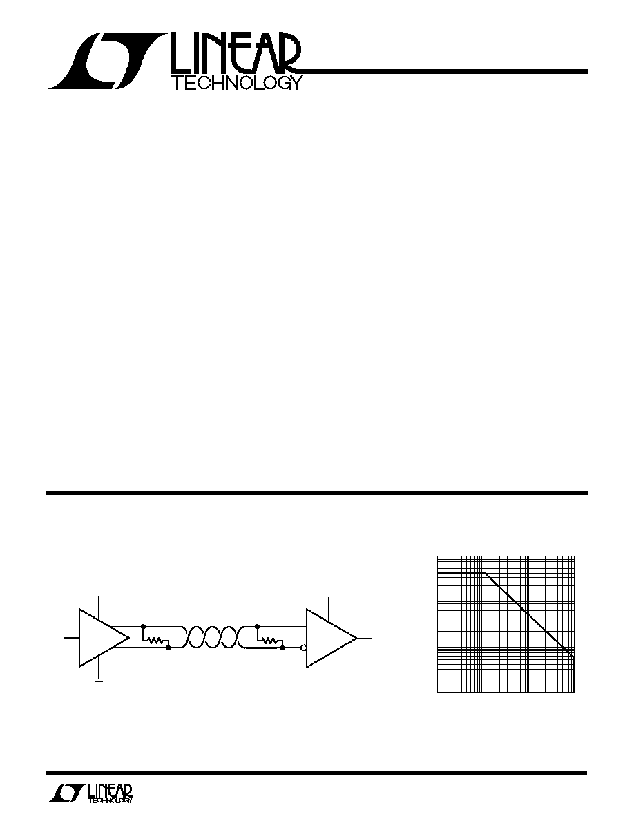
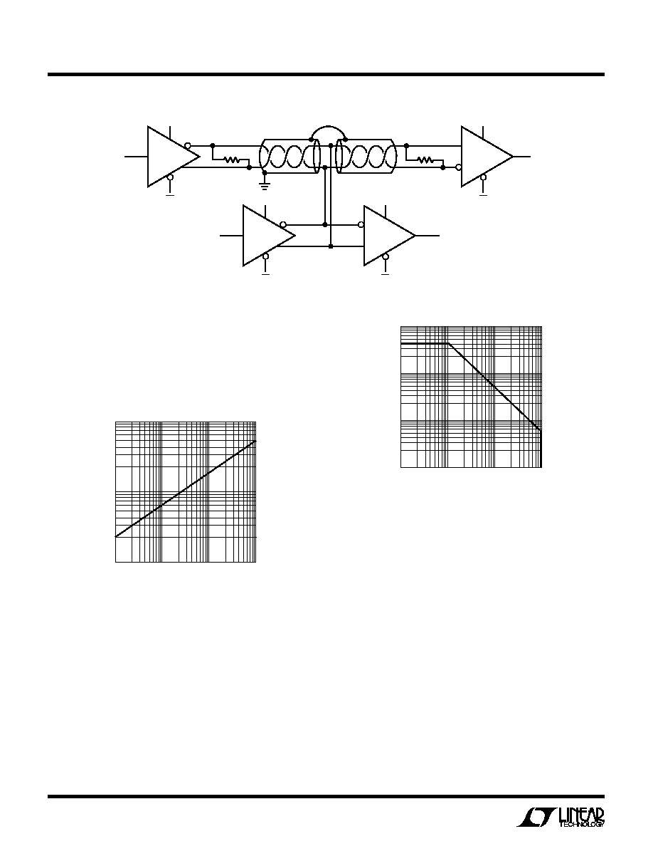
A typical connection of the LTC486 is shown in Figure 6.
A twisted pair of wires connect up to 32 drivers and
receivers for half duplex data transmission. There are no
restrictions on where the chips are connected to the
wires, and it isn't necessary to have the chips connected
at the ends. However, the wires must be terminated only
at the ends with a resistor equal to their characteristic
impedance, typically 120
. The optional shields around
the twisted pair help reduce unwanted noise, and are
connected to GND at one end.
Thermal Shutdown
The LTC486 has a thermal shutdown feature which pro-
tects the part from excessive power dissipation. If the
outputs of the driver are accidently shorted to a power
supply or low impedance source, up to 250mA can flow
through the part. The thermal shutdown circuit disables
the driver outputs when the internal temperature reaches
150
∞
C and turns them back on when the temperature cools
to 130
∞
C. If the outputs of two or more LTC486 drivers are
shorted directly, the driver outputs can not supply enough
current to activate the thermal shutdown. Thus, the ther-
mal shutdown circuit will not prevent contention faults
when two drivers are active on the bus at the same time.
Cable and Data Rate
The transmission line of choice for RS485 applications is
a twisted pair. There are coaxial cables (twinaxial) made for
this purpose that contain straight pairs, but these are less
flexible, more bulky, and more costly than twisted pairs.
Many cable manufacturers offer a broad range of 120
cables designed for RS485 applications.
LTC486 ∑ TA02
A
B
R
R
OD
V
OC
V
LTC486 ∑ TA04
OUTPUT
UNDER TEST
C
L
S1
500
CC
V
S2
LTC486
6
U
S
A
O
PPLICATI
W
U
U
I FOR ATIO
When using low loss cables, Figure 8 can be used as a
guideline for choosing the maximum line length for a given
data rate. With lower quality PVC cables, the dielectric loss
factor can be 1000 times worse. PVC twisted pairs have
terrible losses at high data rates (>100kbs) and greatly
reduce the maximum cable length. At low data rates
however, they are acceptable and much more economical.
Cable Termination
The proper termination of the cable is very important. If the
cable is not terminated with its characteristic impedance,
EN
12
EN
4
LTC486 ∑ TA07
120
DX
1
2
3
SHIELD
120
RX
RX
SHIELD
3
DX
EN
12
EN
4
2
EN
EN
4
1
2
3
RX
RX
3
DX
EN
12
EN
4
1
DX
1/4 LTC488
1/4 LTC486
1/4 LTC488
1/4 LTC486
2
1
12
Losses in a transmission line are a complex combination
of DC conductor loss, AC losses (skin effect), leakage, and
AC losses in the dielectric. In good polyethylene cables
such as the Belden 9841, the conductor losses and dielec-
tric losses are of the same order of magnitude, with
relatively low overall loss (Figure 7).
FREQUENCY (MHz)
0.1
0.1
LOSS PER 100 FT (dB)
1
10
1
10
100
LTC486 ∑ TA08
Figure 7. Attenuation vs Frequency for Belden 9841
DATA RATE (bps)
10k
10
CABLE LENGTH (FT)
100
1k
10k
100k
1M
10M
LTC486 ∑ TA09
2.5M
distorted waveforms will result. In severe cases, distorted
(false) data and nulls will occur. A quick look at the output
of the driver will tell how well the cable is terminated. It is
best to look at a driver connected to the end of the cable,
since this eliminates the possibility of getting reflections
from two directions. Simply look at the driver output while
transmitting square wave data. If the cable is terminated
properly, the waveform will look like a square wave
(Figure 9).
If the cable is loaded excessively (e.g., 47
), the signal
initially sees the surge impedance of the cable and jumps
to an initial amplitude. The signal travels down the cable
and is reflected back out of phase because of the
mistermination. When the reflected signal returns to the
driver, the amplitude will be lowered. The width of the
pedestal is equal to twice the electrical length of the cable
(about 1.5ns/ft). If the cable is lightly loaded (e.g., 470
),
Figure 8. Cable Length vs Data Rate
Figure 6. Typical Connection
7
LTC486
U
S
A
O
PPLICATI
W
U
U
I FOR ATIO
Information furnished by Linear Technology Corporation is believed to be accurate and reliable.
However, no responsibility is assumed for its use. Linear Technology Corporation makes no represen-
tation that the interconnection of its circuits as described herein will not infringe on existing patent rights.
represents an electrical one-tenth wavelength. The value
of the coupling capacitor should therefore be set at 16.3pF
per foot of cable length for 120
cables. With the coupling
capacitors in place, power is consumed only on the signal
edges, not when the driver output is idling at a 1 or 0 state.
A 100nF capacitor is adequate for lines up to 4000 feet in
length. Be aware that the power savings start to decrease
once the data rate surpasses 1/(120
◊
C).
Receiver Open-Circuit Fail-Safe
Some data encoding schemes require that the output of
the receiver maintains a known state (usually a logic 1)
when the data is finished transmitting and all drivers on
the line are forced into three-state. All LTC RS485
receivers have a fail-safe feature which guarantees the
output to be in a logic 1 state when the receiver inputs
are left floating (open-circuit). However, when the cable
is terminated with 120
, the differential inputs to the
receiver are shorted together, not left floating.
If the receiver output must be forced to a known state,
the circuits of Figure 11 can be used.
The termination resistors are used to generate a DC bias
which forces the receiver output to a known state, in this
case a logic 0. The first method consumes about
208mW and the second about 8mW. The lowest power
Figure 10. AC Coupled Termination
Rt
DRIVER
DX
RECEIVER
RX
Rt = 120
Rt = 47
Rt = 470
LTC486 ∑ TA10
PROBE HERE
Figure 9. Termination Effects
the signal reflects in phase and increases the amplitude at
the driver output. An input frequency of 30kHz is adequate
for tests out to 4000 ft. of cable.
AC Cable Termination
Cable termination resistors are necessary to prevent un-
wanted reflections, but they consume power. The typical
differential output voltage of the driver is 2V when the cable
is terminated with two 120
resistors. When no data is
being sent 33mA of DC current flows in the cable . This DC
current is about 220 times greater than the supply current
of the LTC486. One way to eliminate the unwanted current
is by AC coupling the termination resistors as shown in
Figure 10.
LTC486 ∑ TA11
C = LINE LENGTH (FT)
◊
16.3pF
120
RECEIVER
RX
C
LTC486 ∑ TA12
140
RECEIVER
RX
5V
1.5k
RECEIVER
RX
5V
110
130
110
130
120
RECEIVER
RX
C
5V
100k
1.5k
Figure 11. Forcing "0" When All Dirvers Are Off
The coupling capacitor allows high frequency energy to
flow to the termination, but blocks DC and low frequen-
cies. The dividing line between high and low frequency
depends on the length of the cable. The coupling capacitor
must pass frequencies above the point where the line
LTC486
8
U
S
A
O
PPLICATI
W
U
U
I FOR ATIO
Linear Technology Corporation
1630 McCarthy Blvd., Milpitas, CA 95035-7487
(408) 432-1900
q
FAX
: (408) 434-0507
q
TELEX
: 499-3977
NOTE:
1. PIN 1 IDENT, NOTCH ON TOP AND CAVITIES ON THE BOTTOM OF PACKAGES ARE THE MANUFACTURING OPTIONS.
THE PART MAY BE SUPPLIED WITH OR WITHOUT ANY OF THE OPTIONS.
NOTE 1
0.398 ≠ 0.413
(10.109 ≠ 10.490)
(NOTE 2)
16
15
14
13
12
11
10
9
1
2
3
4
5
6
7
8
0.394 ≠ 0.419
(10.007 ≠ 10.643)
0.037 ≠ 0.045
(0.940 ≠ 1.143)
0.004 ≠ 0.012
(0.102 ≠ 0.305)
0.093 ≠ 0.104
(2.362 ≠ 2.642)
0.050
(1.270)
TYP
0.014 ≠ 0.019
(0.356 ≠ 0.482)
TYP
0∞ ≠ 8∞ TYP
NOTE 1
0.005
(0.127)
RAD MIN
0.009 ≠ 0.013
(0.229 ≠ 0.330)
0.016 ≠ 0.050
(0.406 ≠ 1.270)
0.291 ≠ 0.299
(7.391 ≠ 7.595)
(NOTE 2)
◊
45
∞
0.010 ≠ 0.029
(0.254 ≠ 0.737)
2. THESE DIMENSIONS DO NOT INCLUDE MOLD FLASH OR PROTRUSIONS.
MOLD FLASH OR PROTRUSIONS SHALL NOT EXCEED 0.006 INCH (0.15mm).
S Package
16-Lead Plastic SOL
LT/GP 0294 5K REV A ∑ PRINTED IN USA
©
LINEAR TECHNOLOGY CORPORATION 1994
solution is to use an AC termination with a pull-up resistor.
Simply swap the receiver inputs for data protocols ending
in logic 1.
Fault Protection
All of LTC's RS485 products are protected against ESD
transients up to
±
2kV using the human body model
(100pF, 1.5k
). However, some applications need greater
protection. The best protection method is to connect a
bidirectional TransZorb
Æ
from each line side pin to ground
(Figure 12).
A TransZorb
Æ
is a silicon transient voltage suppressor that
has exceptional surge handling capabilities, fast response
time, and low series resistance. They are available from
General Semiconductor Industries and come in a variety of
breakdown voltages and prices. Be sure to pick a break-
down voltage higher than the common-mode voltage
required for your application (typically 12V). Also, don't
forget to check how much the added parasitic capacitance
will load down the bus.
RS232 to RS485 Level Translator with Hysteresis
U
A
O
PPLICATI
TYPICAL
N Package
16-Lead Plastic DIP
0.260 ± 0.010
(6.604 ± 0.254)
0.770
(19.558)
MAX
16
1
2
3
4
5
6
7
8
9
10
11
12
13
14
15
0.015
(0.381)
MIN
0.125
(3.175)
MIN
0.130 ± 0.005
(3.302 ± 0.127)
0.065
(1.651)
TYP
0.045 ≠ 0.065
(1.143 ≠ 1.651)
0.018 ± 0.003
(0.457 ± 0.076)
0.045 ± 0.015
(1.143 ± 0.381)
0.100 ± 0.010
(2.540 ± 0.254)
0.009 ≠ 0.015
(0.229 ≠ 0.381)
0.300 ≠ 0.325
(7.620 ≠ 8.255)
0.325
+0.025
≠0.015
+0.635
≠0.381
8.255
(
)
U
PACKAGE DESCRIPTIO
Dimensions in inches (millimeters) unless otherwise noted.
LTC486 ∑ TA14
120
DRIVER
Y
Z
R = 220k
10k
RS232 IN
5.6k
HYSTERESIS = 10k
◊
VY - VZ
--------
R
19k
----
R
1/4 LTC486
TransZorb
Æ
is a registrated trademark of General Instruments, GSI
LTC486 ∑ TA13
120
DRIVER
Z
Y
Figure 12. ESD Protection