 | ÐлекÑÑоннÑй компоненÑ: LTC487CS | СкаÑаÑÑ:  PDF PDF  ZIP ZIP |
Äîêóìåíòàöèÿ è îïèñàíèÿ www.docs.chipfind.ru
1
LTC487
Quad Low Power
RS485 Driver
D
U
ESCRIPTIO
2
DRIVER
LTC487 · TA01
RECEIVER
DI
EN 12
4
3
1
1/4 LTC487
120
120
RO
3
EN 12
4
2
1
1/4 LTC489
4000 FT BELDEN 9841
s
Very Low Power: I
CC
= 110
µ
A Typ
s
Designed for RS485 or RS422 Applications
s
Single 5V Supply
s
7V to 12V Bus Common-Mode Range Permits
±
7V GND Difference Between Devices on the Bus
s
Thermal Shutdown Protection
s
Power-Up/Down Glitch-Free Driver Outputs Permit
Live Insertion/Removal of Package
s
Driver Maintains High Impedance in Three-State or
with the Power Off
s
28ns Typical Driver Propagation Delays with
5ns Skew
s
Pin Compatible with the SN75174, DS96174,
µ
A96174, and DS96F174
S
FEATURE
The LTC487
®
is a low power differential bus/line driver
designed for multipoint data transmission standard RS485
applications with extended common-mode range ( 7V to
12V). It also meets RS422 requirements.
The CMOS design offers significant power savings over its
bipolar counterpart without sacrificing ruggedness against
overload or ESD damage.
The driver features three-state outputs, with the driver
outputs maintaining high impedance over the entire com-
mon-mode range. Excessive power dissipation caused by
bus contention or faults is prevented by a thermal shut-
down circuit which forces the driver outputs into a high
impedance state.
Both AC and DC specifications are guaranteed from 0
°
C to
70
°
C (Commercial), 40
°
C to 85
°
C (Industrial) and over
the 4.75V to 5.25V supply voltage range.
s
Low Power RS485/RS422 Drivers
s
Level Translator
U
S
A
O
PPLICATI
U
A
O
PPLICATI
TYPICAL
DATA RATE (bps)
10k
10
CABLE LENGTH (FT)
100
1k
10k
100k
1M
10M
LTC487 · TA09
2.5M
* APPLIES FOR 24 GAUGE, POLYETHYLENE
DIELECTRIC TWISTED PAIR
and LTC are registered trademarks and LT is a trademark of Linear Technology Corporation.
RS485 Cable Length Specification*
LTC487
2
ELECTRICAL C
C
HARA TERISTICS
C
D
A
U
G
W
A
W
U
W
A
R
BSOLUTE
XI
TI
S
W
U
U
PACKAGE/ORDER I FOR ATIO
(Note 1)
Supply Voltage (V
CC
) ............................................... 12V
Control Input Voltages .................... 0.5V to V
CC
+ 0.5V
Driver Input Voltages ...................... 0.5V to V
CC
+ 0.5V
Driver Output Voltages ..........................................
±
14V
Control Input Currents ........................................
±
25mA
Driver Input Currents ..........................................
±
25mA
Operating Temperature Range
Commercial ............................................ 0
°
C to 70
°
C
Industrial ........................................... 40
°
C to 85
°
C
Storage Temperature Range ................. 65
°
C to 150
°
C
Lead Temperature (Soldering, 10 sec.)................. 300
°
C
ORDER PART
NUMBER
1
2
3
4
5
6
7
8
16
15
14
13
12
11
10
9
DI1
DO1A
DO1B
EN12
DO2B
DO2A
DI2
GND
DI3
DO3A
DO3B
EN34
DO4B
DO4A
DI4
V
N PACKAGE
16-LEAD PLASTIC DIP
TOP VIEW
CC
S PACKAGE
16-LEAD PLASTIC SOL
T
JMAX
= 125
°
C,
JA
= 70
°
C/W (N)
T
JMAX
= 150
°
C,
JA
= 95
°
C/W (S)
LTC487CN
LTC487CS
LTC487IN
LTC487IS
pins are negative. All voltages are referenced to device GND unless
otherwise specified.
Note 3: All typicals are given for V
CC
= 5V and Temperature = 25
°
C.
Note 1: Absolute maximum ratings are those beyond which the safety of
the device cannot be guaranteed.
Note 2: All currents into device pins are positive; all currents out of device
SYMBOL
PARAMETER
CONDITIONS
MIN
TYP
MAX
UNITS
t
PLH
Driver Input to Output
R
DIFF
= 54
,
C
L1
= C
L2
= 100pF
10
30
50
ns
t
PHL
Driver Input to Output
(Figures 1, 4)
10
30
50
ns
t
SKEW
Driver Output to Output
5
15
ns
t
r,
t
f
Driver Rise or Fall Time
5
20
25
ns
t
ZH
Driver Enable to Output High
C
L
= 100pF (Figures 2, 5) S2 Closed
35
70
ns
t
ZL
Driver Enable to Output Low
C
L
= 100pF (Figures 2, 5) S1 Closed
35
70
ns
t
LZ
Driver Disable Time from Low
C
L
= 15pF (Figures 2, 5) S1 Closed
35
70
ns
t
HZ
Driver Disable Time from High
C
L
= 15pF (Figures 2, 5) S2 Closed
35
70
ns
V
CC
= 5V
±
5%, 0
°
C
T
A
70
°
C (Note 2, 3)
S
U
G C
C
HARA TERISTICS
WITCHI
SYMBOL
PARAMETER
CONDITIONS
MIN
TYP
MAX
UNITS
V
OD1
Differential Driver Output Voltage (Unloaded)
I
O
= 0
5
V
V
OD2
Differential Driver Output Voltage (With Load)
R = 50
; (RS422)
2
V
R = 27
; (RS485) (Figure 3)
1.5
5
V
V
OD
Change in Magnitude of Driver Differential
R = 27
or R = 50
0.2
V
Output Voltage for Complementary Output States
(Figure 3)
V
OC
Driver Common-Mode Output Voltage
3
V
V
OC
Change in Magnitude of Driver Common-Mode
0.2
V
Output Voltage for Complementary Output States
V
IH
Input High Voltage
DI, EN12, EN34
2.0
V
V
IL
Input Low Voltage
0.8
V
I
IN1
Input Current
±
2
µ
A
I
CC
Supply Current
No Load Output Enabled
110
200
µ
A
Output Disabled
110
200
µ
A
I
OSD1
Driver Short-Circuit Current, V
OUT
= High
V
O
= 7V
100
250
mA
I
OSD2
Driver Short-Circuit Current, V
OUT
= Low
V
O
= 12V
100
250
mA
I
OZ
High Impedance State Output Current
V
O
= 7V to 12V
±
10
±
200
µ
A
V
CC
= 5V
±
5%, 0
°
C
T
A
70
°
C (Commercial), 40
°
C
T
A
85
°
C (Industrial) (Note 2, 3)
Consult factory for Military grade parts.
3
LTC487
C
C
HARA TERISTICS
U
W
A
TYPICAL PERFOR
CE
Driver Output High Voltage
Driver Differential Output Voltage
Driver Output Low Voltage
vs Output Current
vs Output Current
vs Output Current
TTL Input Threshold vs Temperature
Driver Skew vs Temperature
Supply Current vs Temperature
TEMPERATURE (
°
C )
50
SUPPLY CURRENT (
µ
A)
90
100
110
120
130
0
50
100
LTC487 · TPC06
TEMPERATURE (
°
C )
50
TIME (ns)
1.0
2.0
3.0
4.0
5.0
0
50
100
LTC487 · TPC05
TEMPERATURE (
°
C )
50
INPUT THRESHOLD VOLTAGE (V)
1.55
1.57
1.59
1.61
1.63
0
50
100
LTC487 · TPC04
Driver Differential Output
Voltage vs Temperature
TEMPERATURE (
°
C )
50
DIFFERENTIAL VOLTAGE (V)
1.5
1.7
1.9
2.1
2.3
0
50
100
LTC487 · TPC07
R
O
= 54
OUTPUT VOLTAGE (V)
0
OUTPUT CURRENT (mA)
0
24
48
72
96
1
2
3
4
LTC487 · TPC01
T
A
= 25°C
OUTPUT VOLTAGE (V)
0
OUTPUT CURRENT (mA)
0
16
32
48
64
1
2
3
4
LTC487· TPC02
T
A
= 25°C
OUTPUT VOLTAGE (V)
0
OUTPUT CURRENT (mA)
0
20
40
60
80
1
2
3
4
LTC487 · TPC03
T
A
= 25°C
LTC487
4
GND (Pin 8): GND connection.
DI3 (Pin 9): Driver 3 input. Refer to DI1.
DO3A (Pin 10): Driver 3 output.
DO3B (Pin 11): Driver 3 output.
EN34 (Pin 12): Driver 3 and 4 outputs enabled. See
Function Table for details.
DO4B (Pin 13): Driver 4 output.
DO4A (Pin 14): Driver 4 output.
DI4 (Pin 15): Driver 4 input. Refer to DI1.
V
CC
(Pin 16): Positive supply; 4.75 < V
CC
< 5.25.
DI1 (Pin 1): Driver 1 input. If Driver 1 is enabled, then a low
on DI1 forces the driver outputs DO1A low and DO1B high.
A high on DI1 with the driver outputs enabled will force
DO1A high and DO1B low.
DO1A (Pin 2): Driver 1 output.
DO1B (Pin 3): Driver 1 output.
EN12 (Pin 4): Driver 1 and 2 outputs enabled. See Func-
tion Table for details.
DO2B (Pin 5): Driver 2 output.
DO2A (Pin 6): Driver 2 output.
DI2 (Pin 7): Driver 2 input. Refer to DI1.
PI
U
FU
U
C
U
S
O
TI
INPUT
ENABLES
OUTPUTS
DI
EN12 or EN34
OUT A
OUT B
H
H
H
L
L
H
L
H
X
L
Z
Z
FU
U
C
UO
TI
TABLE
Figure 2. Driver Enable and Disable Times
H: High Level
L: Low Level
X: Irrelevant
Z: High Impedance (Off)
TI
W
E WAVEFOR
S
U
G
WITCHI
W
S
Figure 1. Driver Propagation Delays
LTC487 · TA06
A, B
EN12
3V
0V
f = 1MHz : t 10ns : t 10ns
V
OL
V
OH
1.5V
1.5V
5V
OUTPUT NORMALLY LOW
t
ZL
2.3V
t
LZ
0.5V
A, B
0V
t
ZH
2.3V
OUTPUT NORMALLY HIGH
t
HZ
0.5V
r
f
V
O
LTC487 · TA05
B
A
DI
V
O
1/2 V
O
3V
0V
t
SKEW
1.5V
t
PLH
1.5V
t
PHL
1/2 V
O
V = V(A) V(B)
V
O
80%
20%
t
f
90%
DIFF
10%
t
SKEW
t
r
f = 1MHz : t 10ns : t 10ns
<
<
r
f
5
LTC487
TEST CIRCUITS
LTC487 · TA04
OUTPUT
UNDER TEST
C
L
S1
500
CC
V
S2
Figure 5. Driver Timing Test Load #2
DRIVER 1
LTC487 · TA03
DI
A
B
EN12
R
DIFF
C
L1
C
L2
Figure 4. Driver Timing Test Circuit
LTC487 · TA02
A
B
R
R
OD
V
OC
V
Figure 3. Driver DC Test Load
U
S
A
O
PPLICATI
W
U
U
I FOR ATIO
Typical Application
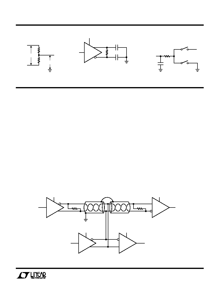
A typical connection of the LTC487 is shown in Figure 6.
A twisted pair of wires connect up to 32 drivers and
receivers for half duplex data transmission. There are no
restrictions on where the chips are connected to the wires,
and it isn't necessary to have the chips connected at the
ends. However, the wires must be terminated only at
the ends with a resistor equal to their characteristic
impedance, typically 120
. The optional shields around
the twisted pair help reduce unwanted noise, and are
connected to GND at one end.
Thermal Shutdown
The LTC487 has a thermal shutdown feature which pro-
tects the part from excessive power dissipation. If the
outputs of the driver are accidently shorted to a power
supply or low impedance source, up to 250mA can flow
through the part. The thermal shutdown circuit disables
the driver outputs when the internal temperature reaches
150
°
C and turns them back on when the temperature
cools to 130
°
C. If the outputs of two or more LTC487
drivers are shorted directly, the driver outputs can not
supply enough current to activate the thermal shutdown.
Thus, the thermal shutdown circuit will not prevent con-
tention faults when two drivers are active on the bus at the
same time.
Cable and Data Rate
The transmission line of choice for RS485 applications is
a twisted pair. There are coaxial cables (twinaxial) made
for this purpose that contain straight pairs, but these are
less flexible, more bulky, and more costly than twisted
pairs. Many cable manufacturers offer a broad range of
120
cables designed for RS485 applications.
Figure 6. Typical Connection
EN12
4
LTC487 · TA07
120
DX
1
2
3
SHIELD
120
RX
RX
SHIELD
3
DX
EN12
4
2
EN12
4
1
2
3
RX
RX
3
DX
EN12
4
1
DX
1/4 LTC489
1/4 LTC487
1/4 LTC489
1/4 LTC487
2
1