Äîêóìåíòàöèÿ è îïèñàíèÿ www.docs.chipfind.ru
LTC5100
1
sn5100 5100fs
FEATURES
APPLICATIO S
U
DESCRIPTIO
U
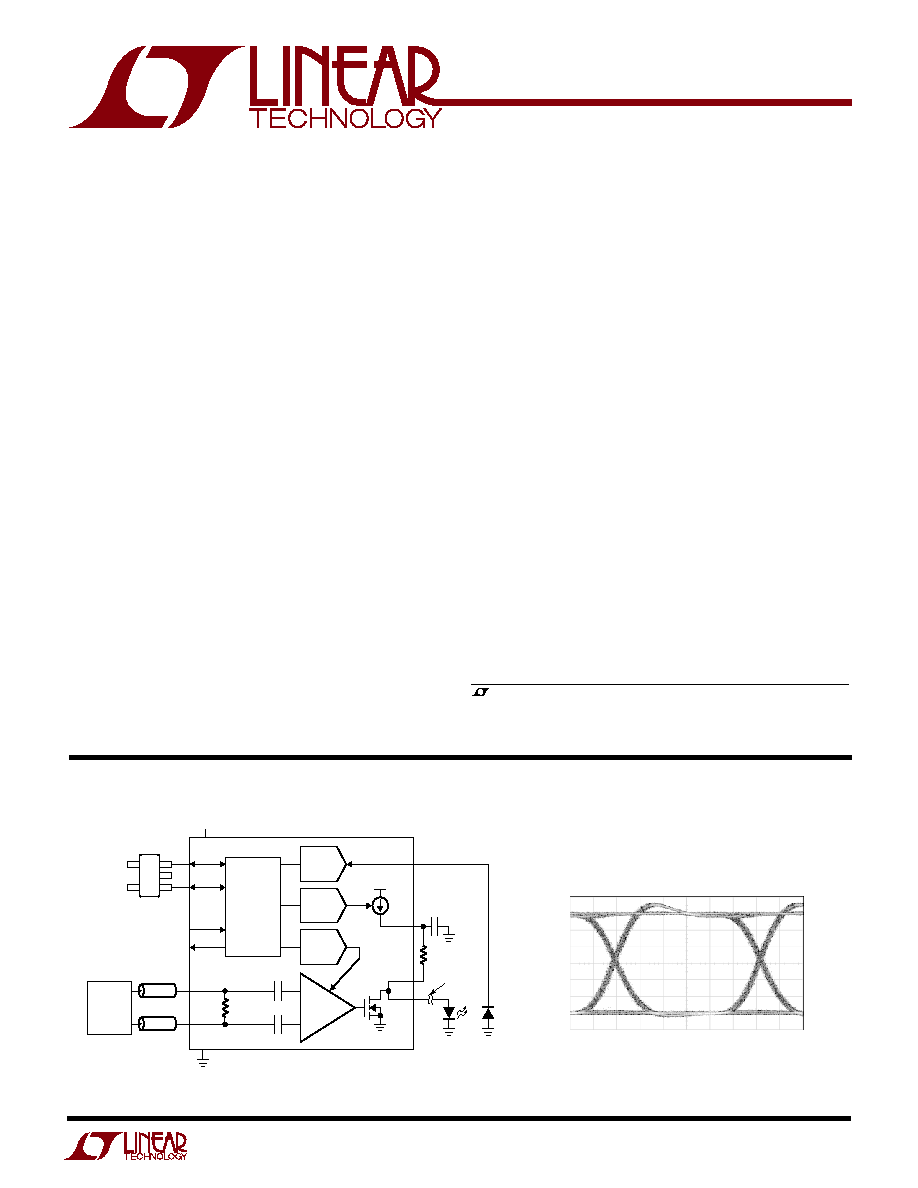
TYPICAL APPLICATIO
U
s
Gigabit Ethernet and Fibre Channel Transceivers
s
SFF and SFP Transceiver Modules
s
Proprietary Fiber Optic Links
, LTC and LT are registered trademarks of Linear Technology Corporation.
s
155Mbps to 3.2Gbps Laser Diode Driver for VCSELs*
s
60ps Rise and Fall Times, 10ps Deterministic Jitter
s
Eye Diagram is Stable and Consistent Across
Modulation Range and Temperature
s
1mA to 12mA Modulation Current
s
Easy Board Layout, Laser can be Remotely Located
if Desired
s
No Input Matching or AC Coupling Components
Needed
s
On-Chip ADC for Monitoring Critical Parameters
s
Digital Setup and Control with I
2
C
TM
Serial Interface
s
Emulation and Set-Up Software Available**
s
Operates Standalone or with a Microprocessor
s
On-Chip DACs Eliminate External Potentiometers
s
Constant Current or Automatic Power Control
s
First and Second Order Temperature Compensation
s
On-Chip Temperature Sensor
s
Extensive Eye Safety Features
s
Single 3.3V Supply
s
4mm
×
4mm QFN Package
3.3V, 3.2Gbps VCSEL Driver
I
2
C is a trademark of Philips Electronics N.V.
*Vertical Cavity Surface Emitting Laser
**Downloadable from www.linear.com
Figure 1. VCSEL Transmitter with Automatic Power Control
The LTC
®
5100 is a 3.2Gbps VCSEL driver offering an
unprecedented level of integration and high speed perfor-
mance. The part incorporates a full range of features to
ensure consistently outstanding eye diagrams. The data
inputs are AC coupled, eliminating the need for external
capacitors. The LTC5100 has a precisely controlled 50
output that is DC coupled to the laser, allowing arbitrary
placement of the IC. No coupling capacitors, ferrite beads
or external transistors are needed, simplifying layout,
reducing board area and the risk of signal corruption. The
unique output stage of the LTC5100 confines the modula-
tion current to the ground system, isolating the high speed
signal from the power supply to minimize RFI.
The LTC5100 supports fully automated production with its
extensive monitoring and control features. Integrated 10-bit
DACs eliminate the need for external potentiometers. An on-
board 10-bit ADC provides the laser current and voltage,
as well as monitor diode current and temperature. Status
information is available from the I
2
C serial interface for feed-
back and statistical process control.
An internal digital controller compensates laser tempera-
ture drift and provides extensive laser safety features.
3.2Gbps Electrical Eye Diagram
1mA/DIV
50ps/DIV
5100 TA01
+
ADC
3.3V
SCL
EN
SDA
V
DD
V
SS
24LC00 EEPROM
IN SOT-23 PACKAGE
MD
MODA
SRC
MODB
DAC
DAC
10nF
3.2Gbps
MODULATOR
FAULT
WARNING: POTENTIAL EYE HAZARD.
SEE "EYE SAFETY INFORMATION"
100
IN
+
IN
50
5100 F01
DIGITAL
CONTROLLER
ARBITRARY
DISTANCE
SERIALIZER
LTC5100
2
sn5100 5100fs
V
DD
, V
DD(HS)
............................................................. 4V
IN
+
, IN
(Cml_en = 1) (Note 6)
Peak Voltage ........... V
DD(HS)
1.2V to V
DD(HS)
+ 0.3V
Average Voltage...... V
DD(HS)
0.6V to V
DD(HS)
+ 0.3V
IN
+
, IN
(Cml_en = 0) (Note 4) .. 0.3V to V
DD(HS)
+ 0.3V
Cml_en = 0 (Note 4)
Peak Difference Between IN
+
and IN
..............
±
2.5V
Average Difference Between IN
+
and IN
.......
±
1.25V
MODA, MODB (Transmitter Disabled) .... 0.3V to 2.75V
MODA, MODB
(Transmitter Enabled) ............ V
DD(HS)
2.75V to 2.75V
EN, SDA, SCL, FAULT ..................... 0.3V to V
DD
+ 0.3V
MD, SRC ................................................... 0.3V to V
DD
Ambient Operating Temperature Range .. 40
°
C to 85
°
C
Storage Temperature Range ................ 65
°
C to 125
°
C
Consult LTC Marketing for parts specified with wider operating temperature ranges.
ABSOLUTE AXI U
RATI GS
W
W
W
U
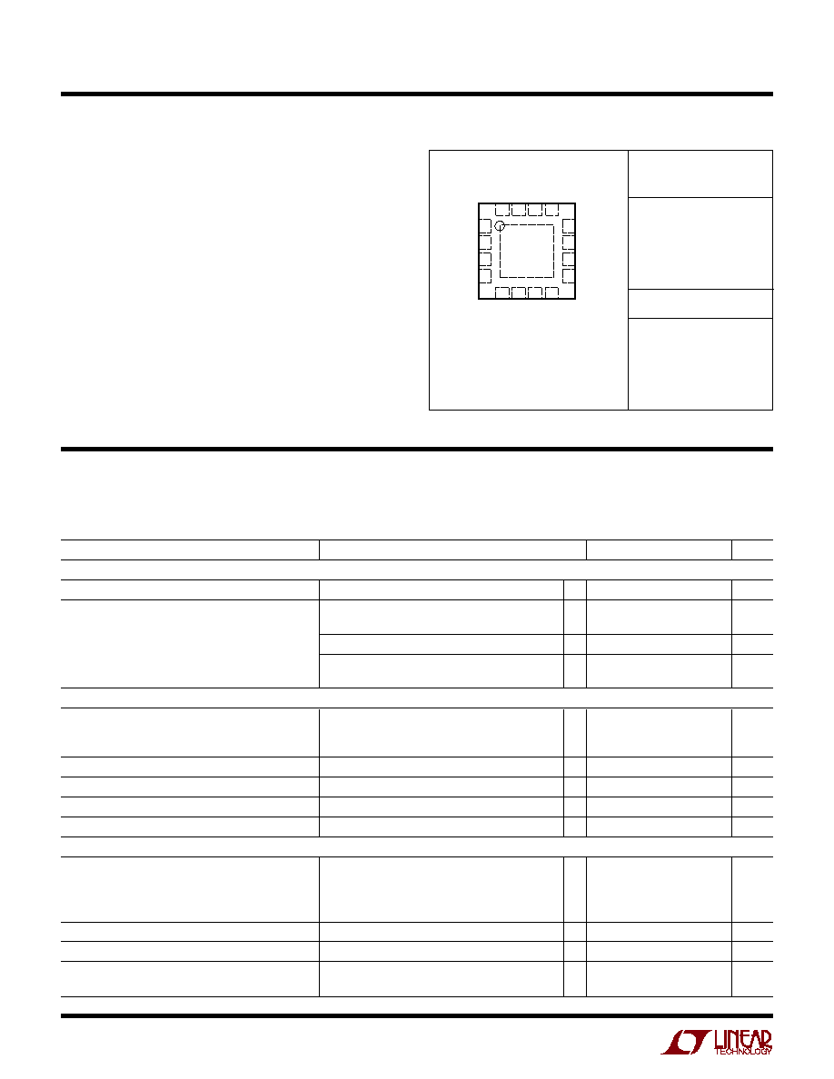
PACKAGE/ORDER I FOR ATIO
U
U
W
(Note 1)
ELECTRICAL CHARACTERISTICS
The
q
denotes the specifications which apply over the full operating
temperature range, otherwise specifications are at T
A
= 25
°
C; V
DD
= V
DD(HS)
= 3.3V, I
S
= 24mA; I
M
= 12mA (I
MPP
= 24mA); 49.9
, 1%
resistor from SRC (Pin 14) to MODA (Pin 11); 50
, 1% load AC coupled to MODB (Pin 10); 10nF, 10% capacitor from SRC (Pin 14) to
V
SS
; Cml_en = 0, Lpc_en = 1, transmitter enabled, unless otherwise noted. Test circuit in Figure 5.
ORDER PART
NUMBER
UF PART MARKING
5100
LTC5100EUF
T
JMAX
= 125
°
C,
JA
= 37
°
C/W
EXPOSED PAD IS V
SS
(PIN 17)
MUST BE SOLDERED TO PCB GROUND PLANE
16 15 14 13
5
6
7
8
TOP VIEW
17
UF PACKAGE
16-LEAD (4mm
×
4mm) PLASTIC QFN
9
10
11
12
4
3
2
1
V
SS
IN
+
IN
V
SS
V
SS
MODA
MODB
V
SS
V
DD
EN
SRC
MD
FAULT
SDA
SCL
V
DD(HS)
1/16 of Full-Scale I
S
Current
PARAMETER
CONDITIONS
MIN
TYP
MAX
UNITS
Power Supply
V
DD
, V
DD(HS)
Operating Voltage
q
3.135
3.3
3.465
V
V
DD
+ V
DD(HS)
Quiescent Current,
V
DD
= 3.465V
Excluding the SRC Pin Current (Note 2)
Transmitter Disabled, Power_down_en = 1
4.5
mA
Transmitter Enabled, Is_rng = Im_rng = 3
54
mA
Impp = 24mA
High Speed Data Inputs (IN
+
and IN
Pins) (Test Circuit, Figure 5)
Input Signal Amplitude
Peak-to-Peak Differential Voltage (The Single-
500 to 2400
mV
P-P
Ended Peak-to-Peak Voltage is One Half the
Differential Voltage)
Common Mode Input Signal Range (Note 3)
Cml_en = 0 (Note 4)
0
V
DD(HS)
V
Differential Input Resistance
80 to 120
Common Mode Input Resistance
Cml_en = 0 (Note 5)
50
k
Open-Circuit Voltage
Cml_en = 0 (Note 5)
1.65
V
SRC Pin Current, I
S
Full-Scale I
S
Current
Is_rng = 0
6
9
mA
Is_rng = 1
12
18
mA
Is_rng = 2
18
27
mA
Is_rng = 3
24
36
mA
Minimum Operating Current (Note 7)
Resolution
10
Bits
SRC Pin Voltage Range
1.2
V
DD
V
200mV
LTC5100
3
sn5100 5100fs
ELECTRICAL CHARACTERISTICS
The
q
denotes the specifications which apply over the full operating
temperature range, otherwise specifications are at T
A
= 25
°
C; V
DD
= V
DD(HS)
= 3.3V, I
S
= 24mA; I
M
= 12mA (I
MPP
= 24mA); 49.9
, 1%
resistor from SRC (Pin 14) to MODA (Pin 11); 50
, 1% load AC coupled to MODB (Pin 10); 10nF, 10% capacitor from SRC (Pin 14) to
V
SS
; Cml_en = 0, Lpc_en = 1, transmitter enabled, unless otherwise noted. Test circuit in Figure 5.
1/8 of Full-Scale Peak-to-Peak
Modulation Current
PARAMETER
CONDITIONS
MIN
TYP
MAX
UNITS
Laser Bias Current, I
B
Full-Scale Current (Note 8)
Is_rng = 0
6 I
M
9 I
M
mA
Is_rng = 1
12 I
M
18 I
M
mA
Is_rng = 2
18 I
M
27 I
M
mA
Is_rng = 3
24 I
M
36 I
M
mA
Absolute Accuracy
SRC Pin and MODA, MODB Pin Currents Within
±
25
%
Specified Voltage Ranges
Resolution
10
Bits
Linear Tempco Resolution
122
ppm/
°
C
Linear Tempco Range
±
15625
ppm/
°
C
Second Order Tempco Resolution
3.81
ppm/
°
C
2
Second Order Tempco Range
±
488
ppm/
°
C
2
Temperature Stability
Ib_tc1 = 0, Ib_tc2 = 0
±
500
ppm/
°
C
Off-State Leakage
Transmitter Disabled, V
SRC
= 1.2V
50
µ
A
MODA, MODB Pin Current, I
M
Full Scale, Peak-to-Peak Modulation Current (Note 9)
Im_rng = 0
6
9
mA
Im_rng = 1
12
18
mA
Im_rng = 2
18
27
mA
Im_rng = 3
24
36
mA
Minimum Operating Current (Note 10)
Resolution (Note 11)
9
Bits
Current Stability
Im_tc1 = 0, Im_tc2 = 0
±
500
ppm/
°
C
Voltage Range
Peak Transient Voltage on MODA and MODB
1.2
2.7
V
Absolute Accuracy of the Modulation Current
±
25
%
Linear Tempco Resolution
122
ppm/
°
C
Linear Tempco Range
±
15625
ppm/
°
C
Second Order Tempco Resolution
3.81
ppm/
°
C
2
Second Order Tempco Range
±
484
ppm/
°
C
2
Maximum Bit Rate
3.2
Gbps
Modulation Current Rise and Fall Times
20% to 80% Measured with K28.5 Pattern at
60
ps
2.5Gbps
Deterministic Jitter, Peak-to-Peak (Note 12)
Measured with K28.5 Pattern at 3.2Gbps
10
ps
Random Jitter, RMS (Note 13)
1
ps
RMS
Pulse Width Distortion
10
ps
Automatic Power Control (Note 14)
Minimum Operating Current for the Monitor Diode
20% of Full Scale
(Note 15)
Monitor Diode Current
Temperature Stability
Imd_tc1 = 0, Imd_tc2 = 0
±
500
ppm/
°
C
Monitor Diode Bias Voltage (Note 16)
I
MD
1600
µ
A
1.45
V
LTC5100
4
sn5100 5100fs
ELECTRICAL CHARACTERISTICS
The
q
denotes the specifications which apply over the full operating
temperature range, otherwise specifications are at T
A
= 25
°
C; V
DD
= V
DD(HS)
= 3.3V, I
S
= 24mA; I
M
= 12mA (I
MPP
= 24mA); 49.9
, 1%
resistor from SRC (Pin 14) to MODA (Pin 11); 50
, 1% load AC coupled to MODB (Pin 10); 10nF, 10% capacitor from SRC (Pin 14) to
V
SS
; Cml_en = 0, Lpc_en = 1, transmitter enabled, unless otherwise noted. Test circuit in Figure 5.
PARAMETER
CONDITIONS
MIN
TYP
MAX
UNITS
Automatic Power Control (Note 14)
Temperature Compensation (Note 17)
Linear Tempco Resolution
254 · Imd_nom/1024
ppm/
°
C
Linear Tempco Range
±
32300 · Imd_nom/1024
ppm/
°
C
ADC
Resolution
10
Bits
Source Current Measurement, I
S
(SRC Pin Current)
Full Scale
Is_rng = 0
9
mA
Is_rng = 1
18
mA
Is_rng = 2
27
mA
Is_rng = 3
36
mA
Accuracy
±
3% of Full Scale
±
25% of Reading
Average Modulation Current Measurement, I
M
(Note 18)
Full Scale
Im_rng = 0
9
mA
Im_rng = 1
18
mA
Im_rng = 2
27
mA
Im_rng = 3
36
mA
Accuracy
±
3% of Full Scale
±
25% of Reading
Laser Diode Voltage Measurement
Full Scale
3.5
V
Accuracy
±
150mV
±
10% of Reading
Monitor Diode Current Measurement (Note 19)
Full Scale
Imd_rng = 0
34
µ
A
Imd_rng = 1
136
µ
A
Imd_rng = 2
544
µ
A
Imd_rng = 3
2176
µ
A
Zero Scale
ADC Code = 0
1/8 of Full Scale
Resolution Relative to Reading
0.2
%
Accuracy
±
25% of Reading
Temperature Measurement
Full Scale
Celsius
239
°
C
Sensitivity
0.500
°
C/LSB
Termination Resistor Voltage Measurement
Full Scale
Is_rng = 0
400
mV
Is_rng = 1
800
mV
Is_rng = 2
1200
mV
Is_rng = 3
1600
mV
Accuracy
±
30mV
±
10% of Reading
Safety Shutdown, Undervoltage Lockout (UVLO)
Undervoltage Detection
V
DD
Decreasing
2.8
V
Undervoltage Detection Hysteresis
150
mV
LTC5100
5
sn5100 5100fs
ELECTRICAL CHARACTERISTICS
The
q
denotes the specifications which apply over the full operating
temperature range, otherwise specifications are at T
A
= 25
°
C; V
DD
= V
DD(HS)
= 3.3V, I
S
= 24mA; I
M
= 12mA (I
MPP
= 24mA); 49.9
, 1%
resistor from SRC (Pin 14) to MODA (Pin 11); 50
, 1% load AC coupled to MODB (Pin 10); 10nF, 10% capacitor from SRC (Pin 14) to
V
SS
; Cml_en = 0, Lpc_en = 1, transmitter enabled, unless otherwise noted. Test circuit in Figure 5.
PARAMETER
CONDITIONS
MIN
TYP
MAX
UNITS
Bias Current Limit, I
B(LIMIT)
Set Point Resolution
7
Bits
Set Point Range
Is_rng = 0
9
mA
Is_rng = 1
18
mA
Is_rng = 2
27
mA
Is_rng = 3
36
mA
Optical Power Limit
Automatic Power Control Mode Only, Apc_en = 1
Overpower Limit
Expressed in % Over the Imd Set Point
50
%
Underpower Limit
Expressed in % Under the Imd Set Point
50
%
Safety Shutdown Response Time
Time from the Fault Occurance to Reduction of
100
µ
s
the Laser Bias Current to 10% of Nominal
FAULT Output, Open-Drain Mode, Flt_drv_mode = 0
Output Low Voltage
I
OL
= 3.3mA
0.4
V
Output High Leakage Current
V
FAULT
= 2.4V
10
µ
A
FAULT Output, Open-Drain Mode with 330
µ
A Internal Pull Up, Flt_drv_mode = 1
Output Low Voltage
I
OL
= 3.3mA
0.4
V
Output High Current
V
FAULT
= 2.4V
280
µ
A
FAULT Output, Open-Drain Mode with 500
µ
A Internal Pull Up, Flt_drv_mode = 2
Output Low Voltage
I
OL
= 3.3mA
0.4
V
Output High Current
V
FAULT
= 2.4V
425
µ
A
FAULT Output, Complementary Drive Mode, Flt_drv_mode = 3
Output High Voltage
I
OH
= 3.3mA
2.4
V
Output Low Voltage
I
OL
= 3.3mA
0.4
V
EN Input, Ib_gain or (Apc_gain in APC Mode) = 16, Im_gain = 4, Is_rng = 0, Im_rng = 0
Input Low Voltage
0.8
V
Input High Voltage
2
V
Input Low Current
En_polarity = 0 (EN Active Low), V
EN
= 0V
10
µ
A
Input High Current
En_polarity = 0 (EN Active Low), V
EN
= V
DD
10 to 10
µ
A
Input Low Current
En_polarity = 1 (EN Active High), V
EN
= 0V
10 to 10
µ
A
Input High Current
En_polarity = 1 (EN Active High), V
EN
= V
DD
10
µ
A
Transmit Enable Time
Time from Active Transition on EN to 95% of
100
ms
Nominal Laser Power and 95% of Full Modulation.
First Time Transmission is Enabled After Power
On or with Rapid_restart_en = 0
Transmit Re-Enable Time
Time from Active Transition on EN to 95% of
1
ms
Nominal Laser Power and 95% of Full Modulation.
When Transmission is Re-Enabled After the First
Time and with Rapid_restart_en = 1
Transmit Disable Time
Time from Inactive Transition on EN to 5% of
10
µ
s
Nominal Laser Power
Minimum Pulse Width Required to Clear
10
µ
s
a Latched Fault