 | –≠–ª–µ–∫—Ç—Ä–æ–Ω–Ω—ã–π –∫–æ–º–ø–æ–Ω–µ–Ω—Ç: REF02H | –°–∫–∞—á–∞—Ç—å:  PDF PDF  ZIP ZIP |

REF-01/REF-02
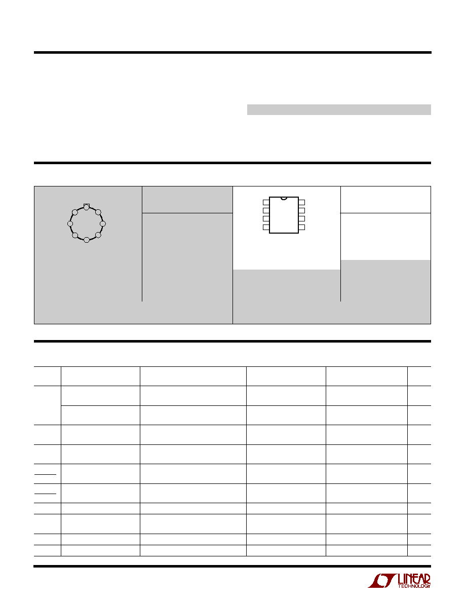
1
15V
≠15V
412
*
1/2W
357
*
1/2W
5V
350
BRIDGE
ACTIVE
ELEMENT
R2
20k
R4
20k
R5
2M
R6
2M**
R3
2M
≠
+
≠
+
GAIN = 100
A2
LT1001
A1
LT307
IN
OUT
GND
REF-02
REDUCES REFERENCE AND AMPLIFIER LOADING.
IF R6 = R3, BRIDGE IS NOT LOADED BY R2 AND R4.
A1 V
OS
AND DRIFT ARE NOT CRITICAL.
*
**
TA01a
≠5V
APPLICATIO S
U
DESCRIPTIO
U
FEATURES
TYPICAL APPLICATIO
U
s
A/D and D/A Converters
s
Precision Regulators
s
Constant Current Sources
s
V/F Converters
s
Bridge Excitation
s
Trimmed Output
±
0.3%
s
Low Drift--5ppm/
∞
C Typ
s
Low Noise--3ppm
(P-P)
s
High Line Rejection
s
Temperature Output--REF-02
s
Low Supply Current 1.4mA Max
Precision
Voltage References
The REF-01/REF-02 are precision 10V and 5V bandgap
references which provide stable output voltages over a
wide range of operating conditions. Output voltage is
accurate to
±
0.3% with a low 5ppm/
∞
C typical temperature
coefficient. The REF-01 and REF-02 are excellent choices
for applications where low drift, moderate accuracy, low
power consumption and low cost are considerations.
The REF-02 includes a temperature output pin which
provides a linear voltage proportional to absolute tem-
perature.
For lower drift and higher accuracy references, please see
the LT1019 and LT1021 data sheets.
, LTC and LT are registered trademarks of Linear Technology Corporation.
Ultra Linear Strain Gauge Amplifier
Output Voltage Temperature Drift
TEMPERATURE (
∞
C)
≠50
OUTPUT VOLTAGE (NORMALIZED)
1.003
1.002
1.001
1.000
0.999
0.998
0.997
25
75
TA01b
≠25
0
50
100
125
0
∞
C TO 70
∞
C BOX GUARANTEED FOR
REF-01E AND REF-02E (8.5ppm/
∞
C)
FULL TEMP RANGE BOX GUARANTEED FOR
REF-01A AND REF-02A (8.5ppm/
∞
C)
REF-01/REF-02
2
REF-01/REF-02 A, E, H ............................................ 40V
REF-01C/REF-02C ................................................... 30V
Power Dissipation .............................................. 500mW
Output Short-Circuit Duration
To Ground ................................................... Indefinite
To V
IN
16V ............................................... Indefinite
To V
IN
> 16V ............................................ Not Allowed
ORDER PART
NUMBER
REF01AH
REF01H
REF01EH
REF01HH
REF01CH
ABSOLUTE AXI U
RATI GS
W
W
W
U
PACKAGE/ORDER I FOR ATIO
U
U
W
(Note 1)
ELECTRICAL CHARACTERISTICS
V
IN
= 15V, T
A
= 25
∞
C unless otherwise noted.
REF-01A/E, REF-02A/E
REF-01H, REF-02H
SYMBOL
PARAMETER
CONDITIONS
MIN
TYP
MAX
MIN
TYP
MAX
UNITS
V
O
Output Voltage
I
L
= 0mA
REF-01
9.97
10
10.03
9.95
10
10.05
V
REF-02
4.985
5
5.015
4.975
5
5.025
V
Output Adjustment Range
R
P
= 10k
REF-01
±
3
5, ≠27
±
3
5, ≠27
%
REF-02
±
3
5, ≠13
±
3
5, ≠13
%
e
nP-P
Output Voltage Noise
0.1Hz to 10Hz (Note 7) REF-01
20
20
µ
V
P-P
REF-02
10
10
µ
V
P-P
V
IN
Input Voltage Range
REF-01
12
40
12
40
V
REF-02
7
40
7
40
V
V
OUT
Line Regulation
(V
OUT
+ 3V)
V
IN
33V
0.0001
0.010
0.0001
0.010
%/V
V
IN
(Note 2)
V
OUT
Load Regulation
I
L
= 0mA to 10mA
REF-01
0.0005
0.008
0.0005
0.010
%/mA
I
OUT
(Note 2)
REF-02
0.0010
0.010
0.001
0.010
%/mA
I
Q
Quiescent Supply Current
No Load
0.65
1.4
0.65
1.4
mA
I
OUT
Load Current
10
20
10
20
mA
Sink Current
≠0.3
≠20
≠0.3
≠20
mA
I
SC
Short-Circuit Current
V
O
= 0V
25
25
mA
V
T
Temperature Voltage Output
(Note 3)
REF-02 Only
620
620
mV
Consult LTC Marketing for parts specified with wider operating temperature ranges.
Storage Temperature Range ................. ≠ 65
∞
C to 150
∞
C
Operating Temperature
REF-01/REF-02, REF-01A/REF-02A ...≠55
∞
C to 125
∞
C
REF-01E/REF-02E, REF-01H/REF-02H,
REF-01C/REF-02C, REF-01D/REF-02D .... 0
∞
C to 70
∞
C
Lead Temperature (Soldering, 10 sec).................. 300
∞
C
ORDER PART
NUMBER
REF02AH
REF02H
REF02EH
REF02HH
REF02CH
REF02DH
TOP VIEW
NC*
NC*
NC*
INPUT
OUTPUT
TRIM
TEMP**
GND (CASE)
8
7
6
5
3
2
1
4
H PACKAGE
8-LEAD TO-5 METAL CAN
*INTERNALLY CONNECTED. DO
NOT CONNECT EXTERNALLY.
**DO NOT CONNECT ON REF-01
T
JMAX
= 150
∞
C,
JA
= 150
∞
C/W,
JC
= 45
∞
C/W
1
2
3
4
8
7
6
5
TOP VIEW
NC*
INPUT
TEMP**
GND
NC*
NC*
OUTPUT
TRIM
N8 PACKAGE
8-LEAD PDIP
J8 PACKAGE
8-LEAD CERDIP
*INTERNALLY CONNECTED. DO
NOT CONNECT EXTERNALLY.
**DO NOT CONNECT ON REF-01
T
JMAX
= 100
∞
C,
JA
= 130
∞
C/W
T
JMAX
= 150
∞
C,
JA
= 100
∞
C/W
REF01EN8
REF01HN8
REF01CN8
REF01EJ8
REF01HJ8
REF01CJ8
REF02EN8
REF02HN8
REF02CN8
REF02DN8
REF02EJ8
REF02HJ8
REF02CJ8
REF02DJ8
OBSOLETE PACKAGE
Consider the N Package for Alternate Source
OBSOLETE PACKAGE
Consider the N Package for Alternate Source

REF-01/REF-02
3
ELECTRICAL CHARACTERISTICS
V
IN
= 15V, T
A
= 25
∞
C unless otherwise noted.
REF-01C, REF-02C
REF-02D
SYMBOL
PARAMETER
CONDITIONS
MIN
TYP
MAX
MIN
TYP
MAX
UNITS
V
O
Output Voltage
I
L
= 0mA
REF-01
9.9
10
10.1
V
REF-02
4.95
5
5.05
4.9
5
5.1
V
Output Adjustment Range
R
P
= 10k
REF-01
5, ≠27
%
REF-02
±
2.7
5, ≠13
±
2
5, ≠13
%
e
nP-P
Output Voltage Noise
0.1Hz to 10Hz (Note 7) REF-01
30
µ
V
P-P
REF-02
12
12
µ
V
P-P
V
OUT
Line Regulation
(V
OUT
+ 3V)
V
IN
33V
0.0001
0.015
0.0001
0.04
%/V
V
IN
(Note 2)
V
OUT
Load Regulation
I
L
= 0mA to 8mA
0.0005
0.015
%/mA
I
OUT
(Note 2)
I
L
= 0mA to 4mA
0.001
0.04
%/mA
I
Q
Quiescent Supply Current
No Load
0.65
1.6
0.65
2
mA
I
OUT
Load Current
8
20
8
20
mA
Sink Current
≠0.2
20
≠0.2
20
mA
I
SC
Short-Circuit Current
V
O
= 0V
25
25
mA
V
T
Temperature Voltage Output
(Note 3)
REF-02 Only
620
620
mV
The
q
denotes the specifications which apply over the full operating temperature range, otherwise specifications are at T
A
= 25
∞
C.
V
IN
= 15V, ≠55
∞
C
T
A
±
125
∞
C for REF-01A/REF-02A and REF-01/REF-02, 0
∞
C
T
A
70
∞
C for REF-01E/REF-02E and
REF-01H/REF-02H, I
L
= 0mA unless otherwise noted.
REF-01A/E, REF-02A/E
REF-01H/REF-02H
SYMBOL
PARAMETER
CONDITIONS
MIN
TYP
MAX
MIN
TYP
MAX
UNITS
V
Output Voltage Change with
0
∞
C
T
A
70
∞
C
0.02
0.06
0.035
0.17
%
T
Temperature (Notes 4, 5)
≠55
∞
C
T
A
125
∞
C
0.09
0.15
0.144
0.45
%
TC
Output Voltage Temperature
(Note 6)
5
8.5
8
25
ppm/
∞
C
Coefficient
Change in V
O
Temperature
R
P
= 10k
0.5
0.5
ppm/%
Coefficient with Output
Adjustment
V
OUT
Line Regulation
0
∞
C
T
A
70
∞
C
0.0001
0.012
0.0001
0.012
%/V
V
IN
(V
OUT
+ 3V)
V
IN
33V (Note 2)
≠55
∞
C
T
A
125
∞
C
0.0001
0.015
0.0001
0.015
%/V
V
OUT
Load Regulation
0
∞
C
T
A
70
∞
C
0.002
0.010
0.002
0.012
%/mA
I
OUT
(I
L
= 0mA to 8mA) (Note 2)
≠55
∞
C
T
A
125
∞
C
0.002
0.012
0.002
0.015
%/mA
Temperature Voltage Output
(Note 3) REF-02
2.1
2.1
mV/
∞
C
Temperature Coefficient

REF-01/REF-02
4
ELECTRICAL CHARACTERISTICS
The
q
denotes the specifications which apply over the full operating
temperature range, otherwise specifications are at T
A
= 25
∞
C. V
IN
= 15V, 0
∞
C
T
A
70
∞
C and I
L
= 0mA unless otherwise noted.
REF-01C, REF-02C
REF-02D
SYMBOL
PARAMETER
CONDITIONS
MIN
TYP
MAX
MIN
TYP
MAX
UNITS
V
Output Voltage Change with
(Notes 4, 5)
0.45
1.7
%
T
Temperature
TC
Output Voltage Temperature
(Note 6)
8
65
8
250
ppm/
∞
C
Coefficient
Change in V
O
Temperature
R
P
= 10k
0.5
0.5
ppm/%
Coefficient with Output
Adjustment
V
OUT
Line Regulation
V
IN
= 8V to 30V
0.0001
0.018
0.0001
0.05
%/V
V
IN
(Note 2)
V
OUT
Load Regulation
I
L
= 0mA to 5mA
0.002
0.018
0.002
0.05
%/mA
I
OUT
(Note 2)
Temperature Voltage Output
(Note 3) REF-02
2.1
2.1
mV/
∞
C
Temperature Coefficient
Note 1: Absolute Maximum Ratings are those values beyond which the life
of a device may be impaired.
Note 2: Line and load regulation specifications include the effect of self
heating.
Note 3: Limit current in or out of Pin 3 to 50nA and capacitance on Pin 3
to 30pF.
Note 4:
V is defined as the absolute difference between the maximum
output voltage and the minimum output voltage over the specified
temperature range expressed as a percentage of nominal output.
V
VMAX VMIN
VOUT
=
≠
∑100
Note 5:
V specification applies trimmed or untrimmed.
Note 6: TC is defined as
V divided by the temperature range, i.e.,
TC
V
TMAX TMIN
=
≠
Note 7: 0.1Hz to 10Hz noise cannot be 100% tested on modern high
speed test equipment, so Linear Technology does not put a guaranteed
maximum specification on this parameter for standard units. 100% bench
testing of 0.1Hz to 10Hz noise is available on special request. To ensure
low output noise, Linear Technology
does 100% test 10Hz to 1kHz noise.
Consult factory for details.

REF-01/REF-02
5
PACKAGE DESCRIPTIO
U
0.050
(1.270)
MAX
0.016 ≠ 0.021**
(0.406 ≠ 0.533)
0.010 ≠ 0.045*
(0.254 ≠ 1.143)
SEATING
PLANE
0.040
(1.016)
MAX
0.165 ≠ 0.185
(4.191 ≠ 4.699)
GAUGE
PLANE
REFERENCE
PLANE
0.500 ≠ 0.750
(12.700 ≠ 19.050)
0.305 ≠ 0.335
(7.747 ≠ 8.509)
0.335 ≠ 0.370
(8.509 ≠ 9.398)
DIA
0.230
(5.842)
TYP
0.027 ≠ 0.045
(0.686 ≠ 1.143)
0.028 ≠ 0.034
(0.711 ≠ 0.864)
0.110 ≠ 0.160
(2.794 ≠ 4.064)
INSULATING
STANDOFF
45
∞
TYP
H8 (TO-5) 0.230 PCD 1197
LEAD DIAMETER IS UNCONTROLLED BETWEEN THE REFERENCE PLANE
AND 0.045" BELOW THE REFERENCE PLANE
FOR SOLDER DIP LEAD FINISH, LEAD DIAMETER IS
0.016 ≠ 0.024
(0.406 ≠ 0.610)
*
**
PIN 1
H Package
8-Lead TO-5 Metal Can (.230 Inch PCD)
(Reference LTC DWG # 05-08-1321)
OBSOLETE PACKAGE

REF-01/REF-02
6
OBSOLETE PACKAGE
J8 Package
8-Lead CERDIP (Narrow .300 Inch, Hermetic)
(Reference LTC DWG # 05-08-1110)
PACKAGE DESCRIPTIO
U
J8 1298
0.014 ≠ 0.026
(0.360 ≠ 0.660)
0.200
(5.080)
MAX
0.015 ≠ 0.060
(0.381 ≠ 1.524)
0.125
3.175
MIN
0.100
(2.54)
BSC
0.300 BSC
(0.762 BSC)
0.008 ≠ 0.018
(0.203 ≠ 0.457)
0
∞
≠ 15
∞
0.005
(0.127)
MIN
0.405
(10.287)
MAX
0.220 ≠ 0.310
(5.588 ≠ 7.874)
1
2
3
4
8
7
6
5
0.025
(0.635)
RAD TYP
0.045 ≠ 0.068
(1.143 ≠ 1.727)
FULL LEAD
OPTION
0.023 ≠ 0.045
(0.584 ≠ 1.143)
HALF LEAD
OPTION
CORNER LEADS OPTION
(4 PLCS)
0.045 ≠ 0.065
(1.143 ≠ 1.651)
NOTE: LEAD DIMENSIONS APPLY TO SOLDER DIP/PLATE
OR TIN PLATE LEADS

REF-01/REF-02
7
N8 1098
0.100
(2.54)
BSC
0.065
(1.651)
TYP
0.045 ≠ 0.065
(1.143 ≠ 1.651)
0.130
±
0.005
(3.302
±
0.127)
0.020
(0.508)
MIN
0.018
±
0.003
(0.457
±
0.076)
0.125
(3.175)
MIN
1
2
3
4
8
7
6
5
0.255
±
0.015*
(6.477
±
0.381)
0.400*
(10.160)
MAX
0.009 ≠ 0.015
(0.229 ≠ 0.381)
0.300 ≠ 0.325
(7.620 ≠ 8.255)
0.325
+0.035
≠0.015
+0.889
≠0.381
8.255
(
)
*THESE DIMENSIONS DO NOT INCLUDE MOLD FLASH OR PROTRUSIONS.
MOLD FLASH OR PROTRUSIONS SHALL NOT EXCEED 0.010 INCH (0.254mm)
N8 Package
8-Lead PDIP (Narrow .300 Inch)
(Reference LTC DWG # 05-08-1510)
PACKAGE DESCRIPTIO
U
Information furnished by Linear Technology Corporation is believed to be accurate and reliable.
However, no responsibility is assumed for its use. Linear Technology Corporation makes no represen-
tation that the interconnection of circuits as described herein will not infringe on existing patent rights.

REF-01/REF-02
8
Linear Technology Corporation
1630 McCarthy Blvd., Milpitas, CA 95035-7417
(408) 432-1900
q
FAX: (408) 434-0507
q
www.linear.com
©
LINEAR TECHNOLOGY CORPORATION 1991
ref012fc LT/CP 0901 1.5K REV C ∑ PRINTED IN USA
RELATED PARTS
PART NUMBER
DESCRIPTION
COMMENTS
LT1019
0.05%, 5ppm/
∞
C Precision Reference
Pin Compatible with the REF-01, REF-02, Improved Specs