1
RH1011
Voltage Comparator
BUR -I CIRCUIT
U
U
The RH1011 is a general purpose comparator with signifi-
cantly better input characteristics than the LM111. Al-
though pin compatible with the LM111, it offers four times
lower bias current, six times lower offset voltage and five
times higher voltage gain.
The wafer lots are processed to Linear Technology's in-
house Class S flow to yield circuits usable in stringent
military applications.
Supply Voltage (Pin 8 to Pin 4)................................ 36V
Output to Negative Supply (Pin 7 to Pin 4) ............. 35V
Ground to Negative Supply (Pin 1 to Pin 4) ............ 30V
Differential Input Voltage ....................................... ± 35V
Voltage at STROBE Pin (Pin 6 to Pin 8) .................... 5V
Input Voltage (Note 1) ....................... Equal to Supplies
Output Short-Circuit Duration ............................. 10 sec
Operating Temperature Range
(Note 2) ........................................... ≠ 55∞C to 125∞C
Storage Temperature Range ................. ≠ 65∞C to 150∞C
Lead Temperature (Soldering, 10 sec) .................. 300∞C
ABSOLUTE
M
AXI
M
U
M
RATINGS
W
W
W
U
DESCRIPTIO
N
U
, LTC and LT are registered trademarks of Linear Technology Corporation.
≠
+
18V
≠18V
2
3
200
1.3k
50k
50k
50k
4
1
8
7
5
≠
+
15V
2V
≠15V
RH1011 BI
3
2
100k
4
1
7
604
8
PACKAGE I FOR ATIO
U
U
W
TOP VIEW
V
+
BALANCE/
STROBE
GND
≠INPUT
OUTPUT
BALANCE
+INPUT
V
≠
8
7
6
5
2
1
4
H PACKAGE
8-LEAD TO-5 METAL CAN
≠
+
3
TOP VIEW
W PACKAGE
10-LEAD CERPAC
1
2
3
4
5
10
9
8
7
6
GND
+INPUT
≠INPUT
NC
V
≠
V
+
OUTPUT
NC
≠
+
BALANCE/
STROBE
BALANCE
1
2
3
4
8
7
6
5
TOP VIEW
GND
+INPUT
≠INPUT
V
≠
V
+
OUTPUT
J8 PACKAGE
8-LEAD CERDIP
BALANCE/
STROBE
BALANCE
OR
2
RH1011
≠ 55∞C T
A
125∞C
(Preirradiation) (Note 10)
TABLE 1: ELECTRICAL CHARACTERISTICS
T
A
= 25∞C
SUB-
SUB-
SYMBOL PARAMETER
CONDITIONS
NOTES
MIN
TYP
MAX
GROUP
MIN
TYP
MAX
GROUP
UNITS
V
OS
Input Offset Voltage
3
1.5
1
3.0
2,3
mV
R
S
50k
4
2.0
1
3.0
2,3
mV
I
OS
Input Offset Curret
4
4
1
6
2,3
nA
I
B
Input Bias Current
3
50
1
80
2,3
nA
4
65
1
80
2,3
nA
V
OS
Input Offset Voltage Drift
T
MIN
T T
MAX
5,9
25
µV/∞C
T
A
VOL
Large Signal Voltage Gain
R = 1k to 15V,
200
4
V/mV
≠ 10V V
OUT
14.5V
R = 500 to 5V,
50
4
V/mV
0.5V V
OUT
4.5V
CMRR
Common Mode Rejection
90
1
dB
Ratio
Input Voltage Range
V
S
= ± 15V
8,9
≠ 14.5
13
≠ 14.5
13
V
V
S
= Single 5V
8,9
0.5
3.0
0.5
3.0
V
t
d
Response Time
6,9
250
ns
V
OL
Output Saturation Voltage
V
IN
= 5mV, I
SINK
= 8mA
0.4
1
0.5
2,3
V
V1 = 0V, I
SINK
= 50mA
1.5
1
1.5
2,3
V
Output Leakage Current
V
IN
= 5mV, V1 = ≠ 15V,
10
1
500
2,3
nA
V
OUT
= 20V
Positive Supply Current
4.0
1
mA
Negative Supply Current
2.5
1
mA
Strobe Current
Minimum to Ensure Output
7,9
500
µA
Transisor is Turned Off
Input Capacitance
6
pF
10Krad(Si) 20Krad(Si) 50Krad(Si) 100Krad(Si) 200Krad(Si)
SYMBOL PARAMETER
CONDITIONS
NOTES MIN
MAX
MIN
MAX
MIN MAX
MIN
MAX MIN
MAX UNITS
V
OS
Input Offset Voltage
1.5
1.5
1.5
1.5
2
mV
I
OS
Input Offset Current
4
4
4
20
50
nA
I
B
Input Bias Current
50
100
150
200
300
nA
A
VOL
Large-Signal Voltage Gain
R = 1k to 15V
200
200
150
100
50
V/mV
≠ 10V V
OUT
14.5V
CMRR
Common Mode Rejection
90
90
90
90
86
dB
Ratio
Input Voltage Range
V
S
= ± 15V
8,9
≠ 14.5
13
≠ 14.5
13
≠ 14.5
13
≠ 14.5
13
≠ 14.5
13
V
V
S
= Single 5V
0.5
3.0
0.5
3.0
0.5
3.0
0.5
3.0
0.5
3.0
V
V
OL
Output Saturation Voltage
V
IN
= 5mV, I
SINK
= 8mA
0.4
0.4
0.4
0.4
0.4
V
V
IN
= 0V, I
SINK
= 50mA
1.5
1.5
1.5
1.5
1.5
V
Output Leakage Current
V
IN
= 5mV, V1 = ≠ 15V
10
10
100
100
100
nA
V
OUT
= 20V
TABLE 1A: ELECTRICAL CHARACTERISTICS
(Postirradiation) (Note 10)
3
RH1011
Information furnished by Linear Technology Corporation is believed to be accurate and reliable.
However, no responsibility is assumed for its use. Linear Technology Corporation makes no represen-
tation that the interconnection of its circuits as described herein will not infringe on existing patent rights.
TABLE 1A: ELECTRICAL CHARACTERISTICS
10Krad(Si) 20Krad(Si) 50Krad(Si) 100Krad(Si) 200Krad(Si)
SYMBOL PARAMETER
CONDITIONS
NOTES MIN
MAX
MIN
MAX
MIN MAX
MIN
MAX MIN
MAX UNITS
Positive Supply Current
4.0
4.0
4.0
4.0
4.0
mA
Negative Supply Current
2.5
2.5
2.5
2.5
2.5
mA
Strobe Current
Minimum to Ensure Output
7,9
500
500
500
500
500
µA
Transistor is Truned Off
Input Capacitance
6 (Typ) 6 (Typ) 6 (Typ) 6 (Typ) 6 (Typ)
pF
(Postirradiation) (Note 10)
MIL-STD-883 TEST REQUIREMENTS
SUBGROUP
Final Electrical Test Requirements (Method 5004)
1*,2,3,4
Group A Test Requirements (Method 5005)
1,2,3,4
Group C and D End Point Electrical Parameters
1
(Method 5005)
* PDA Applies to subgroup 1. See PDA Test Notes.
PDA Test Notes
The PDA is specified as 5% based on failures from group A, subgroup 1,
tests after cooldown as the final electrical test in accordance with method
5004 of MIL-STD-883 Class B. The verified failures (including Delta
parameters) of group A, subgroup 1, after burn-in divided by the total
number of devices submitted for burn-in in that lot shall be used to
determine the percent for the lot.
Linear Technology Corporation reserves the right to test to tighter limits
than those given.
TABLE 2: ELECTRICAL TEST REQUIRE E TS
UW
Note 1: Inputs may be clamped to supplies with diodes so that maximum
input voltage actually exceeds supply voltage by one diode drop. See Input
Protection discussion in the LT
Æ
1011 data sheet.
Note 2: T
JMAX
= 150∞C.
Note 3: Output is sinking 1.5mA with V
OUT
= 0V.
Note 4: These specifications apply for all supply voltages from a single 5V
to ± 15V, the entire input voltage range and for both high and low output
states. The high state is I
SINK
100µA, V
OUT
( V
+
≠ 1V) and the low state
is I
SINK
0.8V. Therefore, this specication defines a worst-case error band
that includes effects due to common mode signals, voltage gain and
output load.
Note 5: Drift is calculated by dividing the offset difference measured at
minimum and maximum temperatures by the temperature difference.
Note 6: Response time is measured with a 100mV step and 5V overdrive.
The output load is a 500 resistor tied to 5V. Time measurement is taken
when the output crosses 1.4V.
Note 7: Do not short the STROBE pin to ground. It should be current
driven at 3mA to 5mA for the shortest strobe time. Currents as low as
500µA will strobe the RH1011 if speed is not important. External leakage
on the STROBE pin in excess of 0.2µA when the strobe is "off " can cause
offset voltage shifts.
Note 8: See graph, Input Offset Voltage vs Common Mode Voltage on the
LT1011 data sheet.
Note 9: Guaranteed by design, characterization or correlation to other
tested parameters.
Note 10: V
S
= ± 15V, V
CM
= 0V, R
S
= 0 , T
A
= 25∞C, V1 = ≠ 15V, output at
Pin 7, unless otherwise noted.
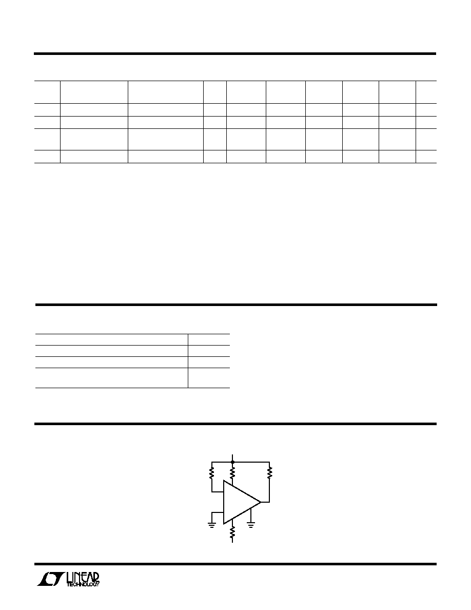
≠
+
12V
5.1k
≠12V
RH1011 TDBC
2
3
4
1
7
8
12
12
5.1k
TOTAL DOSE BIAS CIRCUIT
4
RH1011
Linear Technology Corporation
1630 McCarthy Blvd., Milpitas, CA 95035-7417
(408) 432-1900
q
FAX
: (408) 434-0507
q
TELEX
: 499-3977
©
LINEAR TECHNOLOGY CORPORATION 1989
LT/HP 0896 REV A 500 ∑ PRINTED IN USA
I.D. No. 66-10-0159 Rev. A 0896
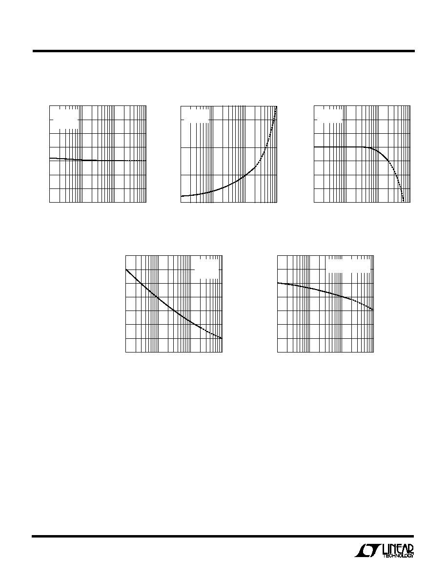
TYPICAL PERFOR
M
A
N
CE CHARACTERISTICS
U
W
Input Offset Voltage
Input Offset Current
Input Bias Current
TOTAL DOSE KRAD (Si)
1
INPUT OFFSET VOLTAGE (mV)
8
6
4
2
0
≠2
≠4
≠6
10
100
1000
RH1011 G01
V
S
=
±
15V
R
S
= 0
V
CM
= 0V
TOTAL DOSE KRAD (Si)
1
INPUT BIAS CURRENT (nA)
300
200
100
0
10
100
1000
RH1011 G02
V
S
=
±
15V
V
CM
= 0V
TOTAL DOSE KRAD (Si)
1
INPUT OFFSET CURRENT (nA)
30
20
10
0
≠10
≠20
≠30
≠40
10
100
1000
RH1011 G03
V
S
=
±
15V
V
CM
= 0V
Voltage Gain
Common Mode Rejection Ratio
TOTAL DOSE KRAD (Si)
1
VOLTAGE GAIN (V/mV)
700
600
500
400
300
200
100
0
10
100
1000
RH1011 G04
V
S
=
±
15V
R
L
= 1k
V
CM
= 0V
TOTAL DOSE KRAD (Si)
1
COMMON MODE REJECTION RATIO (dB)
130
120
110
100
90
80
70
60
10
100
1000
RH1011 G05
V
S
=
±
15V
V
CM
= 14.5V TO 13V