10-31
INFRARED
PRODUCTS
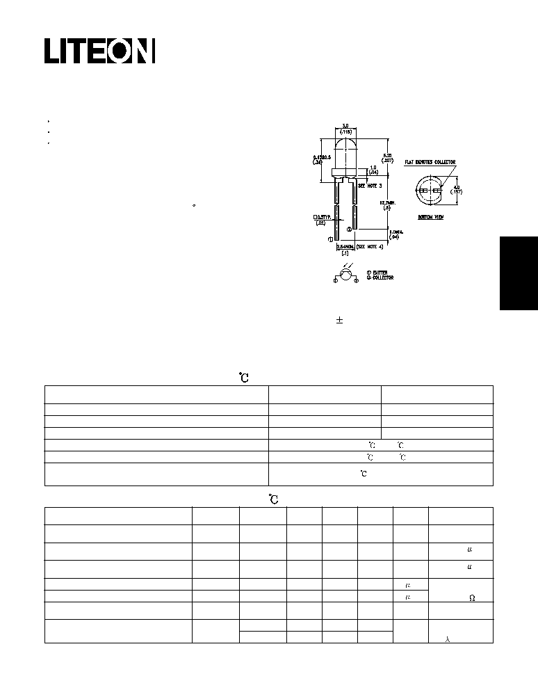
Package Dimensions
Notes:
1. All dimensions are in millimeters (inches).
2. Tolerance is
0.25mm (.010") unless otherwise noted.
3. Protruded resin under flange is 1.5mm (.059") max.
4. Lead spacing is measured where the leads emerge from
the package.
5. Specifications are subject to change without notice.
NPN T-1 Standard
Phototransistor
LTR-4206/LTR-4206E
Features
Wide range of collector currents.
Lens for high sensitivity.
Low cost plastic package.
Description
T h e L T R - 4 2 0 6 s e r i e s c o n s i s t o f a N P N s i l i c o n
phototransistor mounted in a lensed, clear plastic, end
looking package. The lensing effect of the package
allows an acceptance half angle of 10
measured from
the optical axis to the half power point. This series is
mechanically and spectrally matched to the LTE-4206
series of infrared emitting diodes. The LTR-4206E is a
special dark plastic package that cut the visible light
and suitable for the detectors of infrared application.
Parameter
Power Dissipation
Collector-Emitter Voltage
Emitter-Collector Voltage
Operating Temperature Range
Storage Temperature Range
Lead Soldering Temperature
[1.6mm (.063 in.) from body]
260
for 5 Seconds
100
30
5
mW
V
V
-40
to +85
-55
to +100
Maximum Rating
Unit
Parameter
Symbol
Min.
Typ.
Max.
Unit
T e s t
Condition
Collector-Emitter Breakdown Voltage
Emitter-Collector Breakdown Voltage
Collector Emitter Saturation Voltage
Rise Time
Fall Time
Collector Dark Current
On State Collector Current
V
(BR)CEO
V
(BR)ECO
V
CE(SAT)
Tr
Tf
I
CEO
I
C(ON)
30
5
1
1
10
15
4
2
0.4
100
V
V
V
S
S
nA
mA
I
C
=1mA
Ee=0mW/cm
2
I
E
=100
A
Ee=0mW/cm
2
I
C
=100
A
Ee=1mW/cm
2
V
CC
=5V
I
C
=1mA
R
L
=1K
V
CE
=10V
Ee=0mW/cm
2
V
CE
=5V
Ee=1mW/cm
2
=940nm
Absolute Maximum Ratings at Ta=25
Electrical Optical Characteristics at Ta=25
Part No.
LTR-4206
LTR-4206E
