12-96
Ordering Information
Part Number
Package
Safety Standard Approval
Application part
number
LTV-8141
LTV-8141M
LTV-8141S
LTV-8141S-TA
LTV-8141S-TA1
LTV8141-V
LTV8141M-V
LTV8141S-V
LTV8141STA-V
LTV8141STA1-V
LTV-8241
LTV-8241M
LTV-8241S
LTV-8241S-TA
LTV-8241S-TA1
LTV-8441
LTV-8441M
LTV-8441S
LTV-8441S-TA
LTV-8441S-TA1
LTV8241-V
LTV8241M-V
LTV8241S-V
LTV8241STA-V
LTV8241STA1-V
LTV8441-V
LTV8441M-V
LTV8441S-V
LTV8441STA-V
LTV8441STA1-V
4-pin DIP
4-pin (leads with 0.4" spacing)
4-pin (lead bends for surface mount)
4-pin (tape and reel packaging of type I)
4-pin (tape and reel packaging of type II)
8-pin DIP
8-pin (leads with 0.4" spacing)
8-pin (lead bends for surface mount)
8-pin (tape and reel packaging of type I)
8-pin (tape and reel packaging of type II)
16-pin DIP
16-pin (leads with 0.4" spacing)
16-pin (lead bends for surface mount)
16-pin (tape and reel packaging of type I)
16-pin (tape and reel packaging of type II)
UL approved
TUV approved
CSA approved
FIMKO approved
NEMKO approved
SEMKO approved
DEMKO approved
VDE approved
LTV-8141
LTV-8241
LTV-8441
LTV-8141
LTV-8241
LTV-8441
Note:
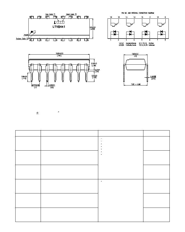
1.Year date code.
2. 2-digit work week.
3. Factory code shall be marked (Z : Taiwan, Y : Thailand).
4. All dimensions are in millimeters (inches).
5. Tolerance is
0.25mm (.010 ) unless otherwise noted.
6. Specifications are subject to change without notice.
PHO
T
OCOUPLER
12-97
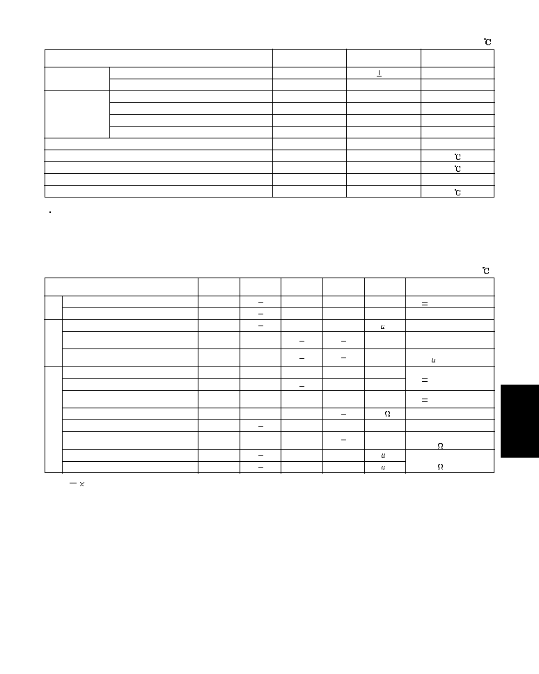
Electrical/Optical Characteristics
(Ta=25
)
Parameter Symbol Min. Typ. Max. Unit Conditions
Input
Output
Transfer
Characteristics
Forward Voltage
Terminal Capacitance
Collector Dark Current
Collector-Emitter
Breakdown Voltage
Emitter-Collector
Breakdown Voltage
Collector Current
*Current Transfer Ratio
Collector-emitter
Saturation Voltage
Isolation Resistance
Floating Capacitance
Cut-off Frequency
Response Time (Rise)
Response Time (Fall)
V
F
C
t
I
CEO
BV
CEO
BV
ECO
I
C
CTR
V
CE(sat)
R
ISO
C
f
f
c
t
r
t
f
35
6
6
600
50
1
1.2
50
0.8
100
0.6
6
60
53
1.4
250
1
75
7,500
1.0
1.0
300
250
V
pF
A
V
V
mA
%
V
G
pF
KHz
s
s
Absolute Maximum Ratings
(Ta=25
)
Parameter
Symbol Rating Unit
Input
Output
Total Power Dissipation
Operating Temperature
Storage Temperature
*1.Isolation Voltage
*2.Soldering Temperature
Forward Current
Power Dissipation
Collector-Emitter Voltage
Emitter-Collector Voltage
Collector Current
Collector Power Dissipation
I
F
P
V
CEO
V
ECO
I
C
P
C
P
tot
T
opr
T
stg
V
iso
T
sol
50
70
35
6
80
150
200
-30~+100
-55~+125
5
260
mA
mW
V
V
mA
mW
mW
KV
rms
*1. AC for 1 minute, R.H. = 40 ~ 60%
Isolation voltage shall be measured using the following method.
(1)Short between anode and cathode on the primary side and between collector, emitter and base on the secondary side.
(2)The isolation voltage tester with zero-cross circuit shall be used.
(3)The waveform of applied volttage shall be a sine wave.
*2. For 10 seconds.
I
F
=
20mA
V=0, f=1KHz
V
CE
=10V
I
C
=0.1mA
I
E
=10
A
I
F
=
1mA V
CE
=2V
I
F
=
20mA, I
C
=5mA
DC500V, 40~60% R.H.
V=0, f=1MHz
V
CE
=5V, I
C
=2mA
R
L
=100
, -3dB
V
CE
=2V, I
C
=10mA
R
L
=100
*CTR=
100%
I
C
I
F