Q
2L
Series SIDACtor
Æ
Device
Data Sheets
Features:
∑
RoHS compliant
∑
Chip Scale Package (CSP) sizing
∑
Wide range of I
PP
ratings including:
75A for 5x310/10x700µs ITU/YDT waveform
80A for 10x1000µs GR 1089 waveform
100A for 10x560µs TIA-968
∑
Bidirectional transient voltage protection
∑
Small footprint (QFN)
∑
Teccor
Æ
brand SIDACtor technology
∑
Recognized under UL E133083 file number
www.littelfuse.com ∑ +1 (800) 999-9445
©2005 Littelfuse ∑ Telecom Design Guide
1
Protection solution to meet:
∑
YD/T 950
∑
YD/T 993
∑
YD/T 1082
∑
GR 1089 Inter-building
∑
IEC 61000-4-5
∑
ITU K.20/21
∑
TIA/EIA-IS-968
Basic Recommendations
Electrical Parameters
Part Number
Marking
XXXX
VDRM
@ldrm=5µA
VS
@100V/µs
IH
IS
IT
VT
@IT=1 amp
Capacitance
@1MHz, 2V bias
Volts
Volts
mAmps
mAmps
Amps
Volts
pF
Min
Max
Min
Max
Min
Max
P0080Q12ALRP
P-8A
6
25
50
800
2.2
5
25
55
P0300Q12ALRP
P03A
25
40
50
800
2.2
5
15
35
P0640Q12ALRP
P06A
58
77
150
800
2.2
5
40
60
P0720Q12ALRP
P07A
65
88
150
800
2.2
5
40
60
P0900Q12ALRP
P09A
75
98
150
800
2.2
5
35
55
P1100Q12ALRP
P11A
90
130
150
800
2.2
5
30
50
P1300Q12ALRP
P13A
120
160
150
800
2.2
5
25
45
P1500Q12ALRP
P15A
140
180
150
800
2.2
5
25
40
P1800Q12ALRP
P18A
170
220
150
800
2.2
5
25
35
P2300Q12ALRP
P23A
190
260
150
800
2.2
5
25
35
P2600Q12ALRP
P26A
220
300
150
800
2.2
5
25
35
P3100Q12ALRP
P31A
275
350
150
800
2.2
5
20
35
P3500Q12ALRP
P35A
320
400
150
800
2.2
5
20
30
P0080Q12BLRP
P08B
6
25
50
800
2.2
5
25
55
P0300Q12BLRP
P03B
25
40
50
800
2.2
5
15
35
P0640Q12BLRP
P06B
58
77
150
800
2.2
5
40
60
P0720Q12BLRP
P07B
65
88
150
800
2.2
5
40
60
P0900Q12BLRP
P09B
75
98
150
800
2.2
5
35
55
P1100Q12BLRP
P11B
90
130
150
800
2.2
5
30
50
P1300Q12BLRP
P13B
120
160
150
800
2.2
5
25
45
P1500Q12BLRP
P15B
140
180
150
800
2.2
5
25
40
P1800Q12BLRP
P18B
170
220
150
800
2.2
5
25
35
P2300Q12BLRP
P23B
190
260
150
800
2.2
5
25
35
P2600Q12BLRP
P26B
220
300
150
800
2.2
5
25
35
P3100Q12BLRP
P31B
275
350
150
800
2.2
5
20
35
P3500Q12BLRP
P35B
320
400
150
800
2.2
5
20
30
PIN 2
PIN 1
The Q
2L
SIDACtor series provides bidirectional transient voltage protection in a low
profile, chip scale package. The small package QFN (Quad Flatpak No-Lead) is ideal
for dense board applications such as line cards, modems, phones, fax machines, and
other telecommunication equipment.
∑ All measurements are made at an ambient temperature of 25∞C. IPP
applies to -40∞C through +85∞C temperature range.
∑ IPP is a repetitive surge rating and is guaranteed for the life of the
product.
∑ Listed SIDACtor devices are bidirectional. All electrical parameters
and surge ratings apply to forward and reverse polarities.
∑ VS is measured at 100 V/µs.
∑ Off-state capacitance is measured at 1MHz with a 2 V bias and is a
typical value for "A" and "B" rated product.
www.littelfuse.com ∑ +1 (800) 999-9445
©2005 Littelfuse ∑ Telecom Design Guide
2
Data
Sheets
Surge Ratings
Series
Ipp
ITSM
di/dt
2x10
µs
1.2x50
µs/8x20µs
10x160
µs
10x560
µs
10x1000
µs
AC 60Hz
Amps
Amps
Amps
Amps
Amps
Amps
Amps/µs
Min
Min
Min
Min
Min
Min
Max
A
150
150
90
50
45
20
500
B
250
250
150
100
80
20
500
Q
2L
Series SIDACtor
Æ
Device
I
H
I
T
I
S
I
DRM
V
DRM
V
T
+V
-V
+I
-I
V
S
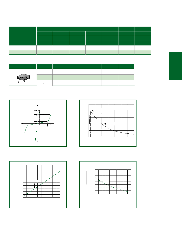
V-I: Characteristics
50
100
0
t
r
t
d
0
Peak
Value
Half Value
t ≠ Time (µs)
I
P
P
≠
P
e
a
k
P
u
l
s
e
C
u
r
r
e
n
t
≠
%
I
P
P
t
r
= rise time to peak value
t
d
= decay time to half value
Waveform = t
r
x t
d
V-I: Pulse Wave-form
-8
-40 -20 0 20 40 60 80 100 120 140 160
-6
-4
0
2
4
6
8
10
12
14
Junction Temperature (T
J
) ≠ ∞C
P
ercent of
V
S
Change ≠
%
25 ∞C
V-I: Junction Temperature
0.4
-40 -20 0 20 40 60 80 100 120 140 160
0.6
0.8
1.0
1.2
1.4
1.6
1.8
2.0
Case Temperature (T
C
) ≠ ∞C
Ratio of
I
H
I
H
(T
C
= 25 ∞C)
25 ∞C
V-I: Holding Current/Case Temperature
Thermal Considerations
Package
Symbol
Parameter
Value
Unit
QFN
TJ
Operating Junction Temperature Range
-40 to +150
∞C
TS
Storage Temperature Range
-65 to +150
∞C
R0JA
Thermal Resistance: Junction to Ambient
120
∞C/W
PIN 2
PIN 1
Data
Sheets
www.littelfuse.com ∑ +1 (800) 999-9445
©2005 Littelfuse ∑ Telecom Design Guide
3
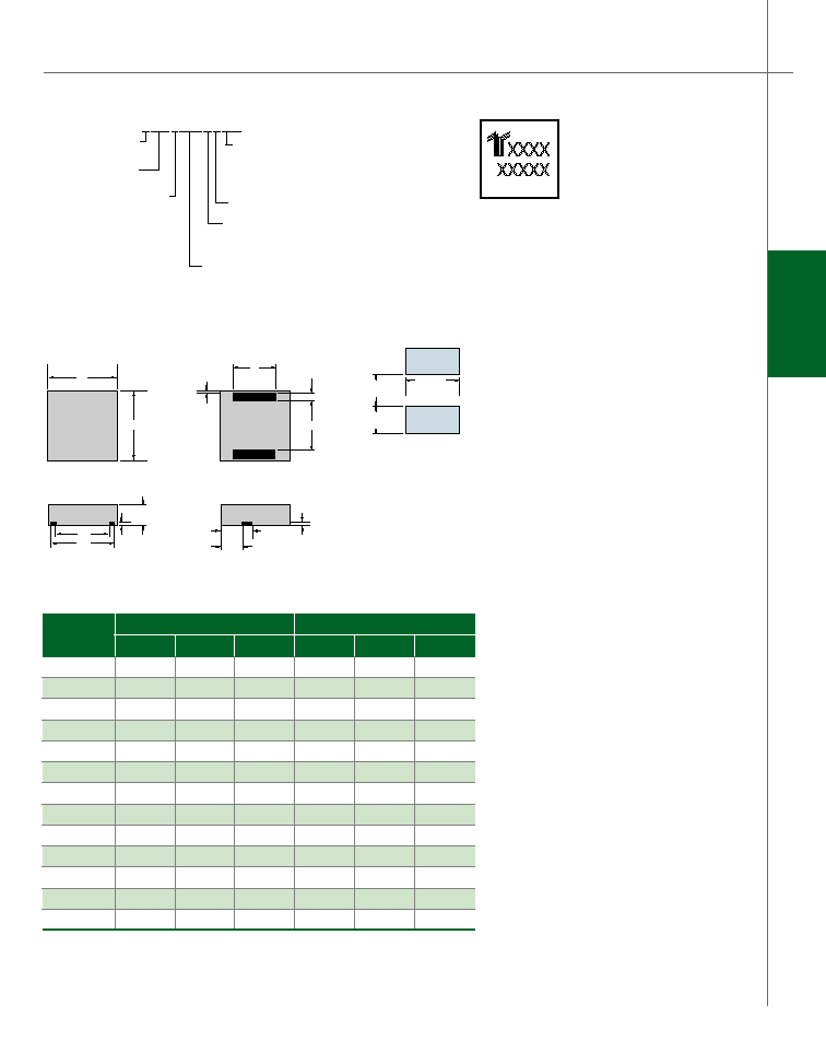
Mechanical Dimensions
Dimensions
Inches
Millimeters
Min
Typ
Max
Min
Typ
Max
A
0.114
0.118
0.122
2.900
3.000
3.100
B
0.114
0.118
0.122
2.900
3.000
3.100
C
0.075
0.079
0.083
1.900
2.000
2.100
E
0.011
0.015
0.019
0.285
0.385
0.485
F
0.076
0.080
0.084
1.930
2.030
2.130
H
0.035
0.039
0.043
0.900
1.000
1.100
J
0.000
0.004
0.008
0.000
0.100
0.200
K1
0.004
0.008
0.012
0.100
0.200
0.300
K2
0.004
0.008
0.012
0.100
0.200
0.300
M1
0.056
0.060
0.064
1.430
1.530
1.630
M2
0.038
0.042
0.046
0.970
1.070
1.170
N1
0.096
0.100
0.104
2.440
2.540
2.640
N2
0.082
0.086
0.090
2.080
2.180
2.280
Q
2L
Series SIDACtor
Æ
Device
2.54
(.100")
H
1.50
(.059")
1.27
(.050")
Can be A or B
K1
N2
N1
END VIEW
SIDE VIEW
M2
M1
K2
F
E
C
J
B
A
TOP VIEW
BOTTOM VIEW
Recommended
Soldering Pad Outline
(Reference Only)
2.54
(.100")
H
1.50
(.059")
1.27
(.050")
Can be A or B
K1
N2
N1
END VIEW
SIDE VIEW
M2
M1
K2
F
E
C
J
B
A
TOP VIEW
BOTTOM VIEW
Recommended
Soldering Pad Outline
(Reference Only)
Part Numbering
CONSTRUCTION VARIATION
0
P
: Single SIDACtor chip used
as a single device
PACKING STYLE
RP : Standard : Embossed carrier tape
SURGE Ipp Rating
A :
50AMP 10x560µs
B : 100AMP 10x560µs
PACKAGE TYPE
Q12 : QFN, 3.0mm x 3.0mm, two leaded package
L : RoHS Compliant
DEVICE TYPE
: SIDACtor
Pxxx0Q12ALRP
MEDIAN VOLTAGE
xxx : xxx volts
and reel per EIA 481-1, 12mm tape in 13" reel.
Device Marking
XXXX
YYYY
First Line: Product Name
Second Line: Lot number
Mechanical Drawings and Recommended Solder Pad Outline
* Reference Tech Brief
(EC642) for soldering
recommendations
Tape and Reel Dimensions
Symbols
Description
Inches
Millimeters
Minimum
Maximum
Minimum
Maximum
A
Reel Diameter
N/A
12.992
N/A
330.0
B
Drive Spoke Width
0.059
N/A
1.50
N/A
C
Arbor Hole Diameter
0.504
0.531
12.80
13.50
D
Drive Spoke Diameter
0.795
N/A
20.20
N/A
N
Hub Diameter
1.969
N/A
50.00
N/A
W1
Reel Inner Width at Hub
0.488
0.567
12.40
14.40
A0
Pocket Width at bottom
0.126
0.134
3.20
3.40
B0
Pocket Length at bottom
0.126
0.134
3.20
3.40
D0
Feed Hole Diameter
0.059
0.063
1.50
1.60
D1
Pocket Hole Diameter
0.059
N/A
1.50
N/A
E1
Feed hole position 1
0.065
0.073
1.65
1.85
E2
Feed hole position 2
0.400
0.408
10.15
10.35
F
Feed hole center-Pocket hole
0.215
0.219
5.45
5.55
K0
Pocket Depth
0.039
0.051
1.00
1.30
P0
Feed Hole Pitch
0.153
0.161
3.90
4.10
P1
Component Spacing
0.311
0.319
7.90
8.10
P2
Feed hole center-Pocket hole
0.077
0.081
1.95
2.05
T
Carrier Tape Thickness
0.010
0.014
0.25
0.35
W
Embossed Carrier Tape Width
0.453
0.484
11.50
12.30
W0
Cover Tape Width
0.358
0.366
9.10
9.30
www.littelfuse.com ∑ +1 (800) 999-9445
©2005 Littelfuse ∑ Telecom Design Guide
4
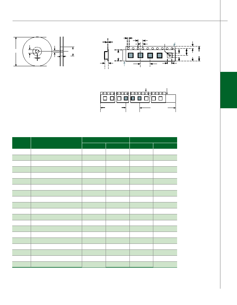
Tape and Reel Dimensional Drawings
Data
Sheets
A
B
D
C
W
1
N
Reel Dimension
K
0
P
0
P
1
W
D
0
A
0
D
1
P
2
E
2
F
W
0
CARRIER TAPE
COVER TAPE
T
E
1
B
0
Tape Dimension Items
TRAILER
160mm MIN
LEADER
400mm MIN
START
END
CARRIER TAPE
COVER TAPE
Tape Leader and Trailer Dimensions
A
B
D
C
W
1
N
Reel Dimension
K
0
P
0
P
1
W
D
0
A
0
D
1
P
2
E
2
F
W
0
CARRIER TAPE
COVER TAPE
T
E
1
B
0
Tape Dimension Items
TRAILER
160mm MIN
LEADER
400mm MIN
START
END
CARRIER TAPE
COVER TAPE
Tape Leader and Trailer Dimensions
Q
2L
Series SIDACtor
Æ
Device