5
SILICON PR
O
TECTION
CIRCUITS
Silicon Protection Circuits
209
w w w . l i t t e l f u s e . c o m
TVS Rail Clamp Diode Array with an Avalanche Diode
SP0506CA, SP0518CAA
This family of rail clamp or "diode steering" arrays are designed for very
low capacitance ESD protection and is offered in small surface mount
packages.
An Avalanche diode has been added between VP and VN
to suppress transients on the supply rails. The multi-channel devices
are used to help protect high speed sensitive digital or analog input
circuits on data, signal, or control lines with unipolar voltage levels up
to 5VDC. The state-of-the-art structure is designed to suppress ESD
and other transient over-voltage events to meet the International
Electrotechnical Compatibility (IEC) transient immunity standards IEC
61000-4-2 for Electrostatic Discharge Requirements.
The monolithic silicon devices are comprised of specially designed
low capacitance structures for transient voltage suppression (TVS).
The size and shape of these structures have be tailored for transient
protection. The very low capacitance and clamp voltage are ideal for
ultra high speed signal line protection.
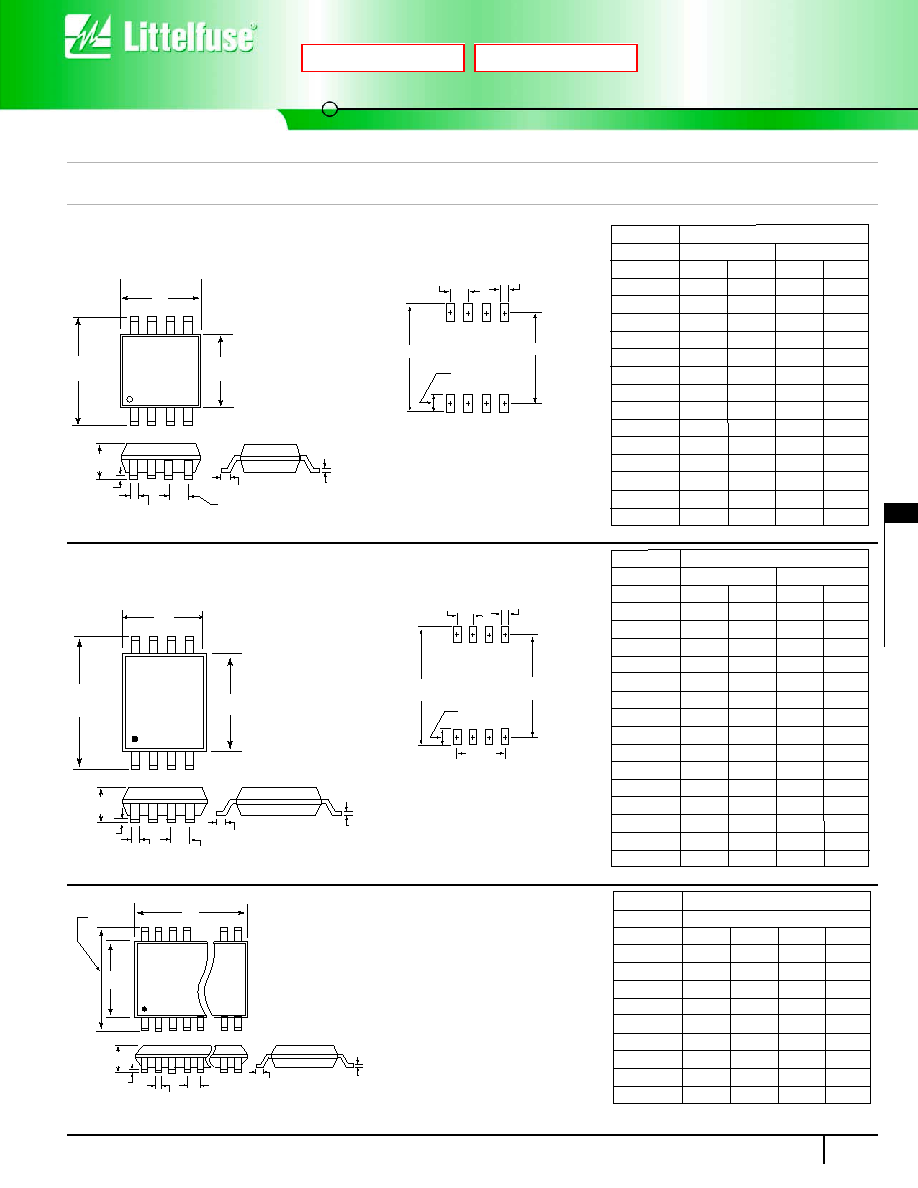
Ordering Information
Schematic
Part Number
SP0506CAAT
SP0506CABT
SP0518CAAT
Quantity Per
Reel
4000
2500
2500
Package Type
MSOP8
SOIC8
QSOP24
CH
6
6
18
1
2
3
4
8
7
6
5
CH 1
CH 2 V-
CH 3
CH 6
V
+
CH 5 CH 4
1 2 3 4 5 6 7 8 9 10 11 12
V
+
CH1 CH2 CH3 CH4 CH5 V
-
CH6 CH7 CH8 CH9 V
+
V
+
CH18 CH17 CH16 CH15 CH14 V
-
CH13 CH12 CH11 CH10 V
+
24 23 22 21 20 19 18 17 16 15 14 13
SP0518CAAT
SP0506CAAT
and
SP0506CABT
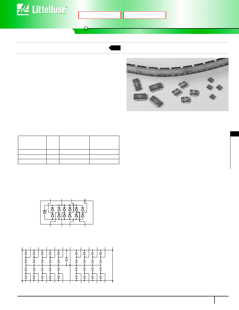
Features
� A low capacitance 2, 6 and 18 channel array of rail
clamp current steering diodes in small surface
mount packages
� ESD Protection Capability (SP0506CA)
- IEC 61000-4-2, Direct Discharge . . . . . . . . . . . . . . . . 8kV (Level 4)
- MIL STD 3015.7. . . . . . . . . . . . . . . . . . . . . . . . . . . . . . . . . . . 15kV
� ESD Protection Capability (SP0518CA)
- IEC 61000-4-2, Direct Discharge . . . . . . . . . . . . . . . 15kV (Level 4)
- MIL STD 3015.7 . . . . . . . . . . . . . . . . . . . . . . . . . . . . . . . . . . 15kV
� Input Protection for Applications Up to 5VDC
� Low Input Capacitance . . . . . . . . . . . . . . . . . . . . . . . . . 3 - 7pF Typical
� Low Clamp Voltage . . . . . . . . . . . . . . . . . . . . . . . . . . Vrail + 13V Max
� Low Input Leakage. . . . . . . . . . . . . . . . . . . . . . . . . . . . . . . 100nA Typ
� Operating Temperature Range . . . . . . . . . . . . . . . . . . . . 20�C to 85�C
Applications
� Computer ports
� Personal Digital Assistants (PDA)
� Portable handheld equipment (Laptop, Palmtop computers)
� Computer port, keyboard (USB1.1)
NEW
Next
Previous
TVS Rail Clamp Diode Array with an Avalanche Diode
SP0506CA, SP0518CAA
Silicon Protection Circuits
210
w w w . l i t t e l f u s e . c o m
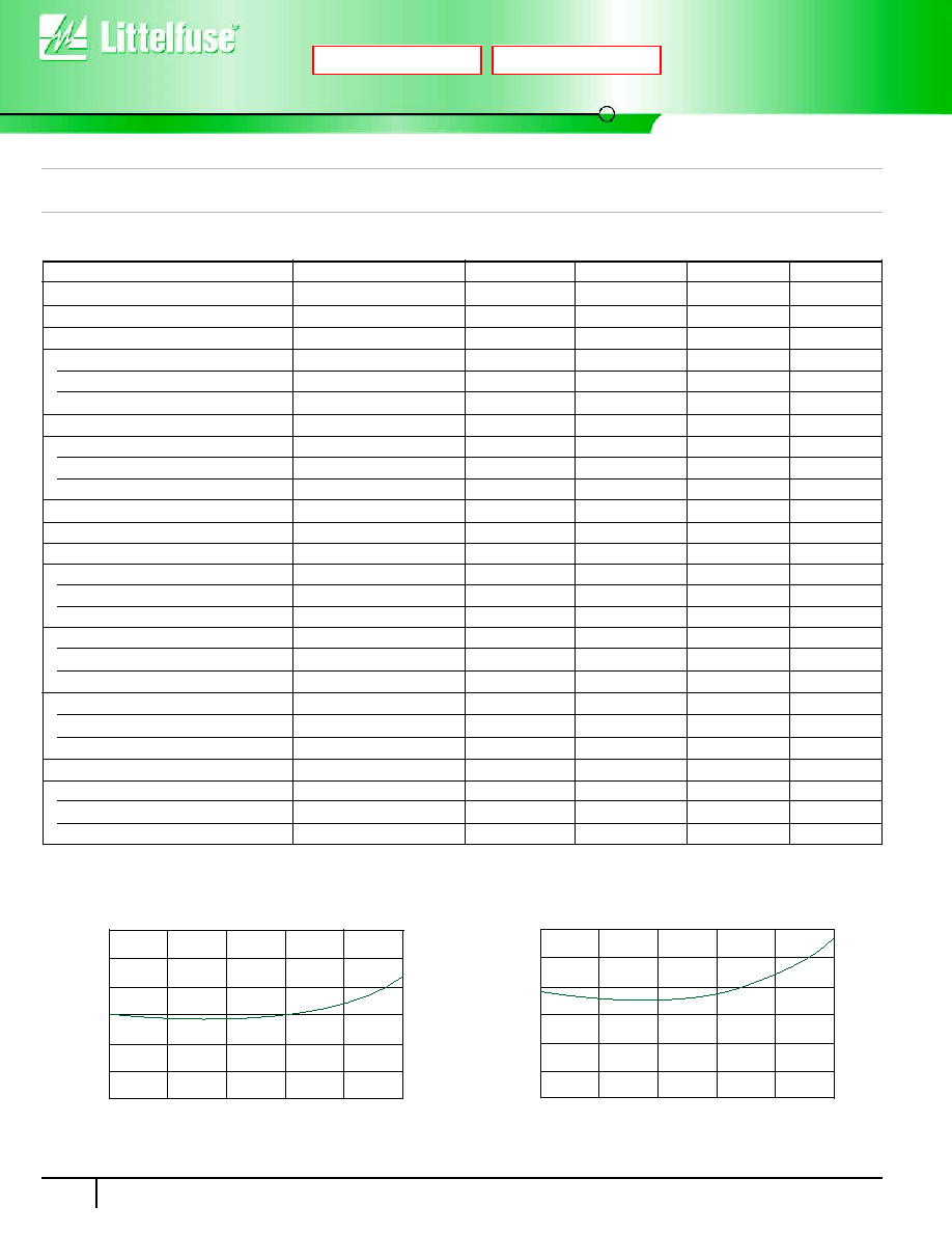
Typical Capacitance
C
IN
(pF)
V
IN
Typical Variation of C
IN
with V
IN
(
V
P
=
5V
,
V
N
=
0
V
,
0.1
�F chip capacitor between V
P
& V
N
)
0
1
2
3
4
5
0
2
4
6
C
IN
(pF)
V
IN
Typical Variation of C
IN
with V
IN
(
V
P
=
5V
,
V
N
=
0
V
,
0.1
�F chip capacitor between V
P
& V
N
)
0
1
2
3
4
5
0
2
4
6
8
10
12
SP0506x
SP0518
Electrical Specifications
T
A
= 25�C Unless Otherwise Specified
PARAMETER
Operating Supply Voltage
Supply Current
Channel Leakage Current
Signal Clamp Voltage
Positive
Negative
Diode Forward Voltage
Maximum Forward current
SP0506x
SP0518
Maximum DC Input voltage
ESD Test Level (SP0506x)
IEC-61000-4-2, Contact discharge
MIL-STD-883 Method 3015 (HBM)
ESD Test Level (SP0518)
IEC-61000-4-2, Contact discharge
MIL-STD-883 Method 3015 (HBM)
Capacitance
SP0506x
SP0518
Turn on/off Time
Temperature Range
Operating
Storage
TEST CONDITIONS
Vp - Vn
Vp - Vn = 5.5V
15kV ESD HBM
2.5VDC @ 1Mhz
2.5VDC @ 1Mhz
MIN
-
0.65
V
N
- 0.5
8
15
15
15
- 20
- 65
MAX
5.5
10
0.1
V
P
+ 13
V
N
- 13
0.95
20
40
V
P
+ 0.5
6
12
+85
+150
UNITS
V
�A
�A
V
V
V
mA
mA
V
kV
kV
kV
kV
pF
pF
ns
�C
�C
TYPICAL
-
0.1
3
7
<1
Next
Previous