 | –≠–ª–µ–∫—Ç—Ä–æ–Ω–Ω—ã–π –∫–æ–º–ø–æ–Ω–µ–Ω—Ç: V22CH8 | –°–∫–∞—á–∞—Ç—å:  PDF PDF  ZIP ZIP |
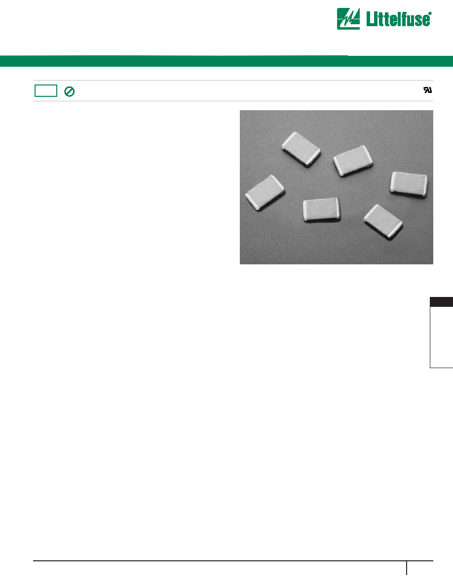
Surface Mount Varistors
195
w w w . l i t t e l f u s e . c o m
Transient Voltage Surge Suppressor
CH Varistor Series
Æ
CH series transient surge suppressors are small, metal-oxide varistors
(MOVs) manufactured in leadless chip form. They are intended for use in a
variety of applications from low voltage DC to off-line board-level protection.
These devices, which have significantly lower profiles than traditional
radial-lead varistors, permit designers to reduce the size and weight and
increase the reliability of their equipment designs.
CH series varistors are available in a voltage range from 14V to
275V VM(AC)RMS , and energy ratings up to 23J.
See the Littelfuse Multilayer Suppressor Series also.
Features
∑ Lead-Free
∑ Leadless, Surface Mount Chip in 5 x 8mm Size
∑ Voltage Ratings VM(AC)RMS,. . . . . . . . . . . . . . . . . . . . . .14V to 275V
∑ Supplied in Tape and Reel or Bulk Pack
∑ No Derating up to 125
o
C Ambient
AGENCY APPROVALS:
Recognized under the components program of
Underwriters Laboratories.
AGENCY FILE NUMBERS:
UL E75961, E135010.
RoHS
Pb
3
SURF
A
CE MOUNT
V
ARIST
ORS
Surface Mount Varistors
196
w w w . l i t t e l f u s e . c o m
Transient Voltage Surge Suppressor
CH Varistor Series
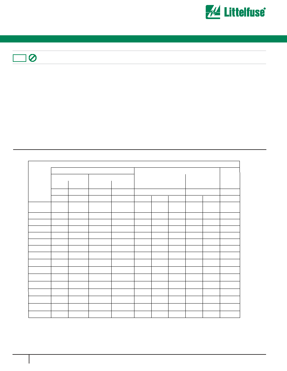
PART
NUMBER
MAXIMUM RATINGS (125
o
C)
SPECIFICATIONS (25
o
C)
CONTINUOUS
TRANSIENT
VARISTOR VOLTAGE AT 1mA
DC TEST CURRENT
MAX CLAMPING
VOLT V
C
AT TEST
CURRENT (8/20
µ
s)
TYPICAL
CAPACI-
TANCE
V
RMS
V
DC
ENERGY
(10/1000
µ
s)
PEAK
CURRENT
(8/20
µ
s)
V
M(AC)
V
M(DC)
W
TM
I
TM
MIN
V
N(DC)
MAX
V
C
I
P
f = 1MHz
(V)
(V)
(J)
(A)
(V)
(V)
(V)
(V)
(A)
(pF)
V22CH8
14
18
(Note 3)
10.0
(Note 2)
250
18.7
22.0
26.0
47
5
1600
V27CH8
17
22
1.0
250
23.0
27.0
31.1
57
5
1300
V33CH8
20
26
1.2
250
29.5
33.0
36.5
68
5
1100
V39CH8
25
31
1.5
250
35.0
39.0
43.0
79
5
900
V47CH8
30
38
1.8
250
42.0
47.0
52.0
92
5
800
V56CH8
35
45
2.3
250
50.0
56.0
62.0
107
5
700
V120CH8
75
102
6.0
500
108.0
120.0
132.0
200
10
300
V150CH8
95
127
8.0
500
135.0
150.0
165.0
250
10
250
V180CH8
115
153
10.0
500
162.0
180.0
198.0
295
10
200
V200CH8
130
175
11.0
500
184.0
200.0
228.0
340
10
180
V220CH8
140
180
12.0
500
198.0
220.0
242.0
360
10
160
V240CH8
150
200
13.0
500
212.0
240.0
268.0
395
10
150
V360CH8
230
300
20.0
500
324.0
360.0
396.0
595
10
100
V390CH8
250
330
21.0
500
354.0
390.0
429.0
650
10
90
V430CH8
275
369
23.0
500
389.0
430.0
473.0
710
10
80
NOTES:
1. Power dissipation of transients not to exceed 0.25W.
2. Energy rating for impulse duration of 30ms minimum to one half of peak current value.
3. Also rated to withstand 24V for 5 minutes.
V150 - V430 CH Varistors are recognized under UL file #E75961 as a recognized component.
V68CH8
40
56
3.0
250
61.0
68.0
75.0
127
10
600
Absolute Maximum Ratings
For ratings of individual members of a series, see Device Ratings and Specifications chart
Continuous:
Steady State Applied Voltage:
AC Voltage Range (VM(AC)RMS) . . . . . . . . . . . . . . . . . . . . . . . . . . . . . . . . . . . . . . . . . . . . . . . . . . . . . . . . . . . . . . . . . . . . . . . . 14 to 275
V
DC Voltage Range (VM(DC)) . . . . . . . . . . . . . . . . . . . . . . . . . . . . . . . . . . . . . . . . . . . . . . . . . . . . . . . . . . . . . . . . . . . . . . . . . . . . 18 to 369
V
Transient:. . . . . . . . . . . . . . . . . . . . . . . . . . . . . . . . . . . . . . . . . . . . . . . . . . . . . . . . . . . . . . . . . . . . . . . . . . . . . . . . . . . . . . . . . . . . . . . . . .
V
Peak Pulse Current (ITM)
For 8/20µs Current Wave (See Figure 2) . . . . . . . . . . . . . . . . . . . . . . . . . . . . . . . . . . . . . . . . . . . . . . . . . . . . . . . . . . . . . . . . . . 250 to 500
A
Single Pulse Energy Range
For 10/1000µs Current Wave (WTM) . . . . . . . . . . . . . . . . . . . . . . . . . . . . . . . . . . . . . . . . . . . . . . . . . . . . . . . . . . . . . . . . . . . . . . 1.0 to 23
J
Operating Ambient Temperature Range (TA) . . . . . . . . . . . . . . . . . . . . . . . . . . . . . . . . . . . . . . . . . . . . . . . . . . . . . . . . . . . . . . . . . . -55 to 125
O
C
Storage Temperature Range (TSTG) . . . . . . . . . . . . . . . . . . . . . . . . . . . . . . . . . . . . . . . . . . . . . . . . . . . . . . . . . . . . . . . . . . . . . . . . -55 to 150
O
C
Temperature Coefficient (
V) of Clamping Voltage (VC) at Specified Test Current . . . . . . . . . . . . . . . . . . . . . . . . . . . . . . . . . . . . . . . <0.01
%/
O
C
CAUTION: Stresses above those listed in "Absolute Maximum Ratings" may cause permanent damage to the device. This is a stress only rating and operation of the device
at these or any other conditions above those indicated in the operational sections of this specification is not implied.
Device Ratings and Specifications
CH SERIES UNITS
Pb
RoHS
Surface Mount Varistors
197
w w w . l i t t e l f u s e . c o m
Transient Voltage Surge Suppressor
CH Varistor Series
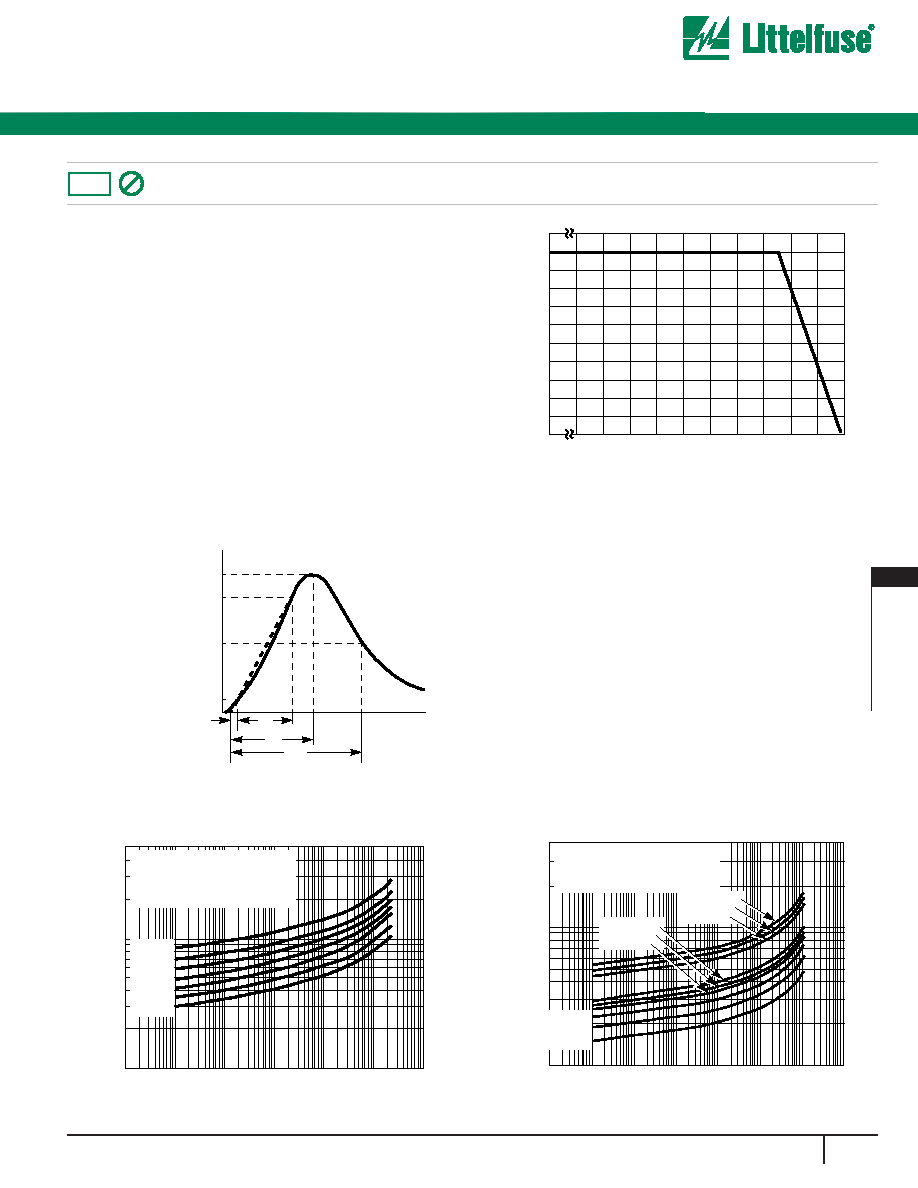
Power Dissipation Ratings
Continuous power dissipation capability is not an applicable design
requirement for a suppressor, unless transients occur in rapid succession.
Under this condition, the average power dissipation required is simply the
energy (watt-seconds) per pulse times the number of pulses per second.
The power so developed must be within the specifications shown on the
Device Ratings and Specifications table for the specific device.
Furthermore, the operating values need to be derated at high tempera-
tures as shown in Figure 1. Because varistors can only dissipate a
relatively small amount of average power they are, therefore, not suitable
for repetitive applications that involve substantial amounts of average
power dissipation.
FIGURE 1. CURRENT, ENERGY AND POWER DERATING
CURVE
100
90
80
70
60
50
40
30
20
10
0
-55
50
60
70
80
90
100
110
120
130
140
150
AMBIENT TEMPERATURE (
o
C)
PERCENT OF RA
TED
V
ALUE
FIGURE 2. PEAK PULSE CURRENT TEST WAVEFORM
100
90
50
10
O
1
T
T
1
T
2
TIME
PERCENT OF PEAK V
ALUE
O
1
= Virtual Origin of Wave
T = Time From 10% to 90% of Peak
T
1
= Virtual Front time = 1.25 ∑ t
T
2
= Virtual Time to Half Value (Impulse Duration)
Example: For an 8/20
µ
s Current Waveform:
8
µ
s = T
1
= Virtual Front Time
20
µ
s = T
2
= Virtual Time to Half Value
FIGURE 3. CLAMPING VOLTAGE FOR V22CH8 - V68CH8
500
400
300
200
100
90
80
70
60
50
40
30
20
10
MAXIMUM PEAK
V
O
L
TS (V)
PEAK AMPERES (A)
10
-3
10
-2
10
-1
10
0
10
1
10
2
10
3
V56CH8
V47CH8
V39CH8
V33CH8
V27CH8
V22CH8
MAXIMUM CLAMPING VOLTAGE
MODEL SIZE 5 x 8mm
22 TO 56V
N(DC)
RATING
T
A
= -55
o
C TO 125
o
C
V68CH8
FIGURE 4. CLAMPING VOLTAGE FOR V120CH8 - V430CH8
4,000
3,000
2,000
1,000
900
800
700
600
500
400
300
200
100
10
-3
10
-2
10
-1
10
0
10
1
10
2
10
3
10
4
V180CH8
V150CH8
V120CH8
V430CH8
V390CH8
V360CH8
V240CH8
V220CH8
V200CH8
PEAK AMPERES (A)
MAXIMUM PEAK
V
O
L
TS (V)
MAXIMUM CLAMPING VOLTAGE
MODEL SIZE 5 x 8mm
100 TO 430V
N(DC)
RATING
T
A
= -55
o
C TO 125
o
C
Transient V-I Characteristics Curves
Pb
RoHS
3
SURF
A
CE MOUNT
V
ARIST
ORS
Surface Mount Varistors
198
w w w . l i t t e l f u s e . c o m
Transient Voltage Surge Suppressor
CH Varistor Series
Recommended Pad Outline
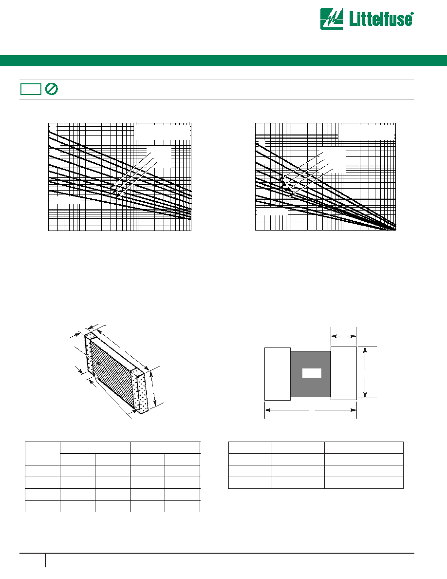
FIGURE 5. SURGE CURRENT RATING CURVES FOR
V22CH8 - V56CH8
500
200
50
20
10
5
2
1
0.2
0.5
100
20
100
1,000
10,000
IMPULSE DURATION (
µ
s)
SURGE CURRENT (A)
1
2
10
10
2
10
3
10
4
10
5
10
6
INDEFINITE
MODEL SIZE 5 x 8mm
V22CH8 - V56CH8
Pulse Rating Curves
FIGURE 6. SURGE CURRENT RATING CURVES FOR
V120CH8 - V430CH8
20
100
1,000
10,000
IMPULSE DURATION (
µ
s)
2,000
1,000
500
200
100
50
20
10
5
2
1
1
2
10
10
2
10
3
10
4
10
5
INDEFINITE
MODEL SIZE 5 x 8mm
V120CH8 - V430CH8
10
6
SURGE CURRENT (A)
NOTE: If pulse ratings are exceeded, a shift of VN(DC) (at specified current) of more than ±10% could result. This type of shift, which normally results in a decrease of VN(DC),
may result in the device not meeting the original published specifications, but it does not prevent the device from continuing to function, and to provide ample protection.
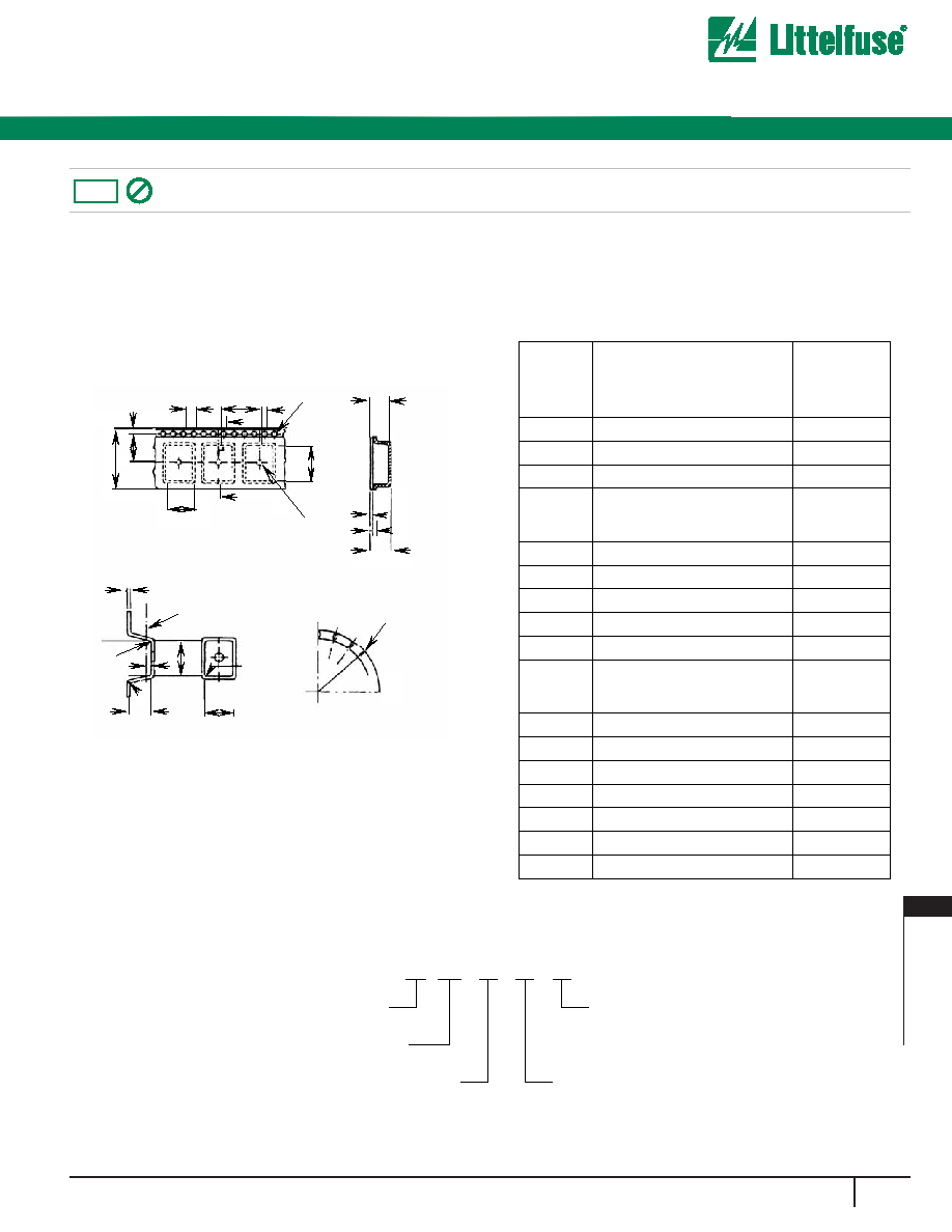
Mechanical Dimensions
E
PASSIVATION
CONTACT AREA
W
L
D
NOTE 1
C
A
B
SYMBOL
INCHES
MILLIMETERS
MIN
MAX
MIN
MAX
D
-
0.080
-
2.03
E
0.016
0.050
0.41
1.27
L
0.311
0.335
7.90
8.51
W
0.185
0.207
4.70
5.26
SYMBOL
INCHES
MILLIMETERS
A
0.402
10.21
B
0.216
5.50
C
0.087
2.21
NOTE: Avoid metal runs in this area. Soldering recommendations:
Material - 62/36/2 Sn/Pb/Ag or equivalent. Temperature - 230
o
C
Max., 5s. Max. Flux - R.M.A.
Pb
RoHS
Surface Mount Varistors
199
w w w . l i t t e l f u s e . c o m
Transient Voltage Surge Suppressor
CH Varistor Series
Standard Packaging
CH Series varistors are always shipped in tape and reel.The standard 13in
reel utilized contains 4000 pieces.
Note also that the CH Series receives no branding on the chip itself.
Tape and Reel Specifications
∑ Conforms to EIA-481, Revision A
∑ Can be Supplied to lEG Publication 286-3
Special Packaging
Option 1
- 7-inch reels containing 1000 pieces are available. To order
7in reels add a T suffix to the part number; e.g., V47CH8T.
Option 2
- For small quantities (less than 100 pieces) the units are
shipped bulk pack. To order, add a S suffix to the part number;
e.g., V47CH8S.
Ordering Information
B
0
D
P
2
P
P
0
A
0
D
1
E
F
W
CROSS SECTION
(REF. PLANE FOR A
0
& B
0
)
T
R
1
R
2
K
0
A
0
R
3
B
0
H
0
K
0
SECTION
THRU
CAVITY
T
1
T
K
MINIMUM
BENDING
RADIUS
R
4
CAVITY DETAILS
REELED RADIUS DETAILS
PLAN VIEW OF STRIP
SYMBOL
PARAMETER
SIZE (mm)
B
0
Cavity Length
8.5
±
0.1
A
0
Cavity Width
5.5
±
0.1
K
0
Cavity Depth
2.0 Min.
H
0
Ref. Plane for A
0
and B
0
+0.10
0.3
-0.05
R
1
, R
2
, R
3
Tape Cavity Radii
0.5 Max.
T
Carrier Tape Thickness
1.0 Max.
T
1
Cover Tape Thickness
0.1 Max.
E
Sprocket Hole from Edge
1.75
±
0.1
P
0
Sprocket Hole Pitch
4.0
±
0.1
D
Sprocket Hole Diameter
+0.1
1.5
-0.0
P
2
Hole Centre to Component Centre
2.0
±
0.15
R
4
Min. Bending Radius
40.0 Min.
D
1
Ejection Hole Diameter
1.5 Min.
K
Overall Thickness
3.0 Min.
P
Pitch Of Component
8.0
±
0.1
F
Sprocket Hole to Ejection Hole
7.5
±
0.1
W
Carrier Tape Width
16.0
±
0.3
V
220
CH
8
RELATIVE SIZE INDICATOR
LITTELFUSE VARISTOR TECHNOLOGY
SERIES DESIGNATOR
NOMINAL VARISTOR VOLTAGE
PACKAGING OPTIONS
No Letter: Standard 13 Inch Reel
T: 7 Inch Reel
S: Bulk Pack
X
Pb
RoHS
3
SURF
A
CE MOUNT
V
ARIST
ORS