
DEVICES INCORPORATED
L10C11
4/8-bit Variable Length Shift Register
Pipeline Registers
03/27/2000≠LDS.11-L
1
u
u
u
u
u Variable Length 4 or 8-bit Wide
Shift Register
u
u
u
u
u Selectable Delay Length from 3 to
18 Stages
u
u
u
u
u Low Power CMOS Technology
u
u
u
u
u Replaces Fairchild TMC2011
u
u
u
u
u Load, Shift, and Hold Instructions
u
u
u
u
u Separate Data In and Data Out Pins
u
u
u
u
u Package Styles Available:
∑ 24-pin Plastic DIP
∑ 28-pin Plastic LCC, J-Lead
FEATURES
DESCRIPTION
L10C11
4/8-bit Variable Length Shift Register
DEVICES INCORPORATED
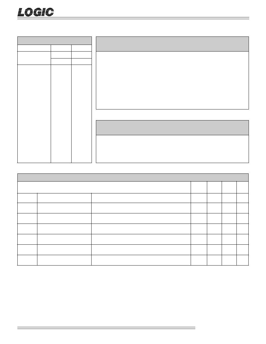
The L10C11 is a high-speed, low
power CMOS variable length shift
register. The L10C11 consists of two
4-bit wide, adjustable length shift
registers. These registers share control
signals and a common clock. Both
shift registers can be programmed
together to any length from 3 to 18
stages inclusive, or one register can be
fixed at 18 stages of delay while the
other is variable. The configuration
implemented is determined by the
Length Code (L
3-0
) and the MODE
control line as shown in Table 1.
Each input is applied to a chain of
registers which are clocked on the
rising edge of the common CLK input.
These registers are numbered R1
through R17 and R1' through R17',
corresponding to the D
3-0
and D
7-4
data fields respectively. A multi-
plexer serves to route the contents of
any of registers R2 through R17 to the
output register, denoted R18. A
similar multiplexer operates on the
contents of R2' through R17' to load
R18'. Note that the minimum-length
path from data inputs to outputs is R1
to R2 to R18, consisting of three stages
of delay.
The MODE input determines whether
one or both of the internal shift
registers have variable length. When
MODE = 0, both D
3-0
and D
7-4
are
delayed by an amount which is
controlled by L
3-0
. When MODE = 1,
the D
7-4
field is delayed by 18 stages
independent of L
3-0
.
The Length Code (L
3-0
) controls the
number of stages of delay applied to
the D inputs as shown in Table 1.
When the Length Code is 0, the inputs
are delayed by 3 clock periods. When
the Length Code is 1, the delay is 4
clock periods, and so forth. The
Length Code and MODE inputs are
latched on the rising edge of CLK.
Both the Length Code and MODE
values may be changed at any time
without affecting the contents of
registers R1 through R17 or R1'
through R17'.
L10C11 B
LOCK
D
IAGRAM
REGISTER R1
REGISTER R2
REGISTER R3
REGISTER R15
REGISTER R16
REGISTER R17
L REGISTER
D
3-0
4
REGISTER R1'
REGISTER R2'
REGISTER R3'
REGISTER R15'
REGISTER R16'
REGISTER R17'
D
7-4
4
L
3-0
MODE
4
CLK
R17
R16
R15
R4
R3
R2
MUX
REGISTER R18
4
Y
3-0
REGISTER R18'
4
Y
7-4
R17'
R16'
R15'
R4'
R3'
R2'
MUX
DEVICES INCORPORATED
L10C11
4/8-bit Variable Length Shift Register
Pipeline Registers
03/27/2000≠LDS.11-L
2
Length Code
Mode = 0
Mode = 1
Delay
Delay
L
3
L
2
L
1
L
0
Y
3-0
Y
7-4
Y
3-0
Y
7-4
0
0
0
0
3
3
3
18
0
0
0
1
4
4
4
18
0
0
1
0
5
5
5
18
0
0
1
1
6
6
6
18
0
1
0
0
7
7
7
18
0
1
0
1
8
8
8
18
0
1
1
0
9
9
9
18
0
1
1
1
10
10
10
18
1
0
0
0
11
11
11
18
1
0
0
1
12
12
12
18
1
0
1
0
13
13
13
18
1
0
1
1
14
14
14
18
1
1
0
0
15
15
15
18
1
1
0
1
16
16
16
18
1
1
1
0
17
17
17
18
1
1
1
1
18
18
18
18
T
ABLE
1.
C
ONTROL
E
NCODING
Storage temperature ..................................................... ≠65∞C to +150∞C
Operating ambient temperature ..................................... ≠55∞C to +125∞C
V
CC
supply voltage with respect to ground ...................... ≠0.5 V to +7.0 V
Input signal with respect to ground .................................. ≠3.0 V to +7.0 V
Signal applied to high impedance output ......................... ≠3.0 V to +7.0 V
Output current into low outputs ....................................................... 25 mA
Latchup current ......................................................................... > 400 mA
M
AXIMUM
R
ATINGS
Above which useful life may be impaired (Notes 1, 2, 3, 8)
O
PERATING
C
ONDITIONS
To meet specified electrical and switching characteristics
Symbol
Parameter
Test Condition
Min
Typ
Max
Unit
V
OH
Output High Voltage
V
CC
= Min., I
OH
= ≠12 mA
2.4
V
V
OL
Output Low Voltage
V
CC
= Min., I
OL
= 24 mA
0.5
V
V
IH
Input High Voltage
2.0
V
CC
V
V
IL
Input Low Voltage
(Note 3)
0.0
0.8
V
I
IX
Input Current
Ground
V
IN
V
CC
(Note 12)
±
20
µA
I
CC1
V
CC
Current, Dynamic
(Notes 5, 6)
10
20
mA
I
CC2
V
CC
Current, Quiescent
(Note 7)
1.0
mA
E
LECTRICAL
C
HARACTERISTICS
Over Operating Conditions (Note 4)
Mode
Temperature Range
Supply Voltage
Active Operation, Com.
0∞C to +70∞C
4.75 V £ V
CC
£ 5.25 V
Active Operation, Mil.
≠55∞C to +125∞C
4.50 V £ V
CC
£ 5.50 V
DEVICES INCORPORATED
L10C11
4/8-bit Variable Length Shift Register
Pipeline Registers
03/27/2000≠LDS.11-L
3
1234567890123456789012345678901212345678901234
1234567890123456789012345678901212345678901234
1234567890123456789012345678901212345678901234
1234567890123456789012345678901212345678901234
1234567890123456789012345678901212345678901234
1234567890123456789012345678901212345678901234
1234567890123456789012345678901212345678901234
1234567890123456789012345678901212345678901234
1234567890123456789012345678901212345678901234
1234567890123456789012345678901212345678901234
1234567890123456789012345678901212345678901234
1234567890123456789012345678901212345678901234
1234567890123456789012345678901212345678901234
1234567890123456789012345678901212345678901234
1234567890123456789012345678901212345678901234
1234567890123456789012345678901212345678901234
1234567890123456789012345678901212345678901234
1234567890123456789012345678901212345678901234
1234567890123456789012345678901212345678901234
1234567890123456789012345678901212345678901234
1234567890123456789012345678901212345678901234
1234567890123456789012345678901212345678901234
1234567890123456789012345678901212345678901234
1234567890123456789012345678901212345678901234
1234567890123456789012345678901212345678901234
1234567890123456789012345678901212345678901234
L10C11≠
30*
25*
20*
Symbol
Parameter
Min
Max
Min
Max
Min
Max
t
PD
Output Delay
30
25
20
t
PW
Clock Pulse Width
15
12
12
t
SD
Data Setup Time
25
10
10
t
HD
Data Hold Time
2
2
0
t
SL
L
3-0
, MODE Setup Time
25
10
10
t
HL
L
3-0
, MODE Hold Time
2
2
0
1234567890123456
1234567890123456
1234567890123456
1234567890123456
1234567890123456
1234567890123456
1234567890123456
1234567890123456
1234567890123456
1234567890123456
1234567890123456
1234567890123456
1234567890123456
1234567890123456
1234567890123456
1234567890123456
1234567890123456
1234567890123456
1234567890123456
1234567890123456
1234567890123456
1234567890123456
1234567890123456
1234567890123456
1234567890123456
1234567890123456
L10C11≠
25*
20
15
Symbol
Parameter
Min
Max
Min
Max
Min
Max
t
PD
Output Delay
25
20
15
t
PW
Clock Pulse Width
15
12
10
t
SD
Data Setup Time
20
10
8
t
HD
Data Hold Time
2
0
0
t
SL
L
3-0
, MODE Setup Time
20
10
8
t
HL
L
3-0
, MODE Hold Time
2
0
0
C
OMMERCIAL
O
PERATING
R
ANGE
(0∞C to +70∞C)
Notes 9, 10 (ns)
SWITCHING CHARACTERISTICS
M
ILITARY
O
PERATING
R
ANGE
(≠55∞C to +125∞C)
Notes 9, 10 (ns)
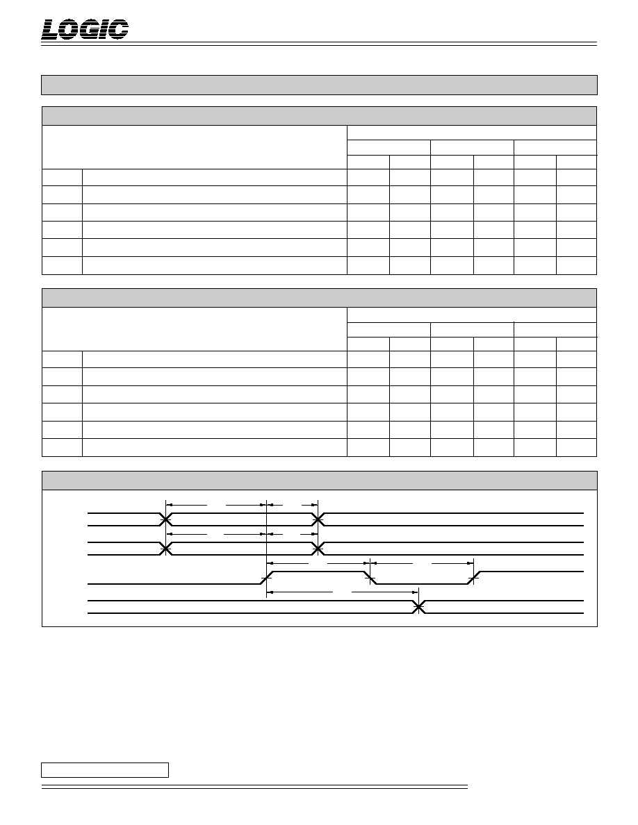
S
WITCHING
W
AVEFORMS
t
SL
CLK
t
SD
t
HD
t
HL
t
PW
t
PW
t
PD
D
7-0
L
3-0
Y
7-0
MODE
123456789012345678901234
123456789012345678901234
123456789012345678901234
123456789012345678901234
*D
ISCONTINUED
S
PEED
G
RADE

DEVICES INCORPORATED
L10C11
4/8-bit Variable Length Shift Register
Pipeline Registers
03/27/2000≠LDS.11-L
4
1. Maximum Ratings indicate stress
specifications only. Functional oper-
ation of these products at values be-
yond those indicated in the Operating
Conditions table is not implied. Expo-
sure to maximum rating conditions for
extended periods may affect reliability.
2. The products described by this speci-
fication include internal circuitry de-
signed to protect the chip from damaging
substrate injection currents and accumu-
lations of static charge. Nevertheless,
conventional precautions should be ob-
served during storage, handling, and use
of these circuits in order to avoid expo-
sure to excessive electrical stress values.
3. This device provides hard clamping of
transient undershoot and overshoot. In-
put levels below ground or above V
CC
will be clamped beginning at ≠0.6 V and
V
CC
+ 0.6 V. The device can withstand
indefinite operation with inputs in the
range of ≠0.5 V to +7.0 V. Device opera-
tion will not be adversely affected, how-
ever, input current levels will be well in
excess of 100 mA.
4. Actual test conditions may vary from
those designated but operation is guar-
anteed as specified.
5. Supply current for a given application
can be accurately approximated by:
where
N = total number of device outputs
C = capacitive load per output
V = supply voltage
F = clock frequency
6. Tested with all outputs changing ev-
ery cycle and no load, at a 5 MHz clock
rate.
7. Tested with all inputs within 0.1 V of
V
CC
or Ground, no load.
8. These parameters are guaranteed
but not 100% tested.
NCV F
4
2
NOTES
9. AC specifications are tested with
input transition times less than 3 ns,
output reference levels of 1.5 V (except
t
DIS
test), and input levels of nominally
0 to 3.0 V. Output loading may be a
resistive divider which provides for
specified I
OH
and I
OL
at an output
voltage of V
OH
min and V
OL
max
respectively. Alternatively, a diode
bridge with upper and lower current
sources of I
OH
and I
OL
respectively,
and a balancing voltage of 1.5 V may be
used. Parasitic capacitance is 30 pF
minimum, and may be distributed.
This device has high-speed outputs ca-
pable of large instantaneous current
pulses and fast turn-on/turn-off times.
As a result, care must be exercised in the
testing of this device. The following
measures are recommended:
a. A 0.1 µF ceramic capacitor should be
installed between V
CC
and Ground
leads as close to the Device Under Test
(DUT) as possible. Similar capacitors
should be installed between device V
CC
and the tester common, and device
ground and tester common.
b. Ground and V
CC
supply planes
must be brought directly to the DUT
socket or contactor fingers.
c. Input voltages should be adjusted to
compensate for inductive ground and V
CC
noise to maintain required DUT input
levels relative to the DUT ground pin.
10. Each parameter is shown as a min-
imum or maximum value. Input re-
quirements are specified from the point
of view of the external system driving
the chip. Setup time, for example, is
specified as a minimum since the exter-
nal system must supply at least that
much time to meet the worst-case re-
quirements of all parts. Responses from
the internal circuitry are specified from
the point of view of the device. Output
delay, for example, is specified as a
maximum since worst-case operation of
any device always provides data within
that time.
11. For the t
ENA
test, the transition is
measured to the 1.5 V crossing point
with datasheet loads. For the t
DIS
test,
the transition is measured to the
±200mV level from the measured
steady-state output voltage with
±10mA loads. The balancing volt-
age, V
TH
, is set at 3.5 V for Z-to-0
and 0-to-Z tests, and set at 0 V for Z-
to-1 and 1-to-Z tests.
12. These parameters are only tested at
the high temperature extreme, which is
the worst case for leakage current.
S1
I
OH
I
OL
V
TH
C
L
DUT
OE
0.2 V
t
DIS
t
ENA
0.2 V
1.5 V
1.5 V
3.5V Vth
1
Z
0
Z
Z
1
Z
0
1.5 V
1.5 V
0V Vth
V
OL
*
V
OH
*
V
OL
*
V
OH
*
Measured V
OL
with I
OH
= ≠10mA and I
OL
= 10mA
Measured V
OH
with I
OH
= ≠10mA and I
OL
= 10mA
F
IGURE
B. T
HRESHOLD
L
EVELS
F
IGURE
A. O
UTPUT
L
OADING
C
IRCUIT
DEVICES INCORPORATED
L10C11
4/8-bit Variable Length Shift Register
Pipeline Registers
03/27/2000≠LDS.11-L
5
1234567890123456789012345678901212345678901234567
1234567890123456789012345678901212345678901234567
1234567890123456789012345678901212345678901234567
1234567890123456789012345678901212345678901234567
1234567890123456789012345678901212345678901234567
1234567890123456789012345678901212345678901234567
1234567890123456789012345678901212345678901234567
1234567890123456789012345678901212345678901234567
1234567890123456789012345678901212345678901234567
1234567890123456789012345678901212345678901234567
1234567890123456789012345678901212345678901234567
1234567890123456789012345678901212345678901234567
1234567890123456789012345678901212345678901234567
1234567890123456789012345678901212345678901234567
1234567890123456789012345678901212345678901234567
1234567890123456789012345678901212345678901234567
1234567890123456789012345678901212345678901234567
1234567890123456789012345678901212345678901234567
1234567890123456789012345678901212345678901234567
1234567890123456789012345678901212345678901234567
1234567890123456789012345678901212345678901234567
1234567890123456789012345678901212345678901234567
1234567890123456789012345678901212345678901234567
1234567890123456789012345678901212345678901234567
1234567890123456789012345678901212345678901234567
1234567890123456789012345678901212345678901234567
1234567890123456789012345678901212345678901234567
1234567890123456789012345678901212345678901234567
1234567890123456789012345678901212345678901234567
1234567890123456789012345678901212345678901234567
1234567890123456789012345678901212345678901234567
1234567890123456789012345678901212345678901234567
1234567890123456789012345678901212345678901234567
1234567890123456789012345678901212345678901234567
1234567890123456789012345678901212345678901234567
1234567890123456789012345678901212345678901234567
1234567890123456789012345678901212345678901234567
1234567890123456789012345678901212345678901234567
1234567890123456789012345678901212345678901234567
1234567890123456789012345678901212345678901234567
1234567890123456789012345678901212345678901234567
1234567890123456789012345678901212345678901234567
1234567890123456789012345678901212345678901234567
1234567890123456789012345678901212345678901234567
1234567890123456789012345678901212345678901234567
1234567890123456789012345678901212345678901234567
1234567890123456789012345678901212345678901234567
1234567890123456789012345678901212345678901234567
1234567890123456789012345678901212345678901234567
1234567890123456789012345678901212345678901234567
1234567890123456789012345678901212345678901234567
1234567890123456789012345678901212345678901234567
1234567890123456789012345678901212345678901234567
1234567890123456789012345678901212345678901234567
1234567890123456789012345678901212345678901234567
1234567890123456789012345678901212345678901234567
1234567890123456789012345678901212345678901234567
1234567890123456789012345678901212345678901234567
1234567890123456789012345678901212345678901234567
1234567890123456789012345678901212345678901234567
1234567890123456789012345678901212345678901234567
1234567890123456789012345678901212345678901234567
1234567890123456789012345678901212345678901234567
1234567890123456789012345678901212345678901234567
1234567890123456789012345678901212345678901234567
1234567890123456789012345678901212345678901234567
1234567890123456789012345678901212345678901234567
1234567890123456789012345678901212345678901234567
1234567890123456789012345678901212345678901234567
Plastic DIP
(P2)
L10C11PC20
L10C11PC15
24-pin -- 0.3" wide
ORDERING INFORMATION
24-pin -- 0.6" wide
0∞C to +70∞C -- C
OMMERCIAL
S
CREENING
Speed
20 ns
15 ns
≠55∞C to +125∞C -- MIL-STD-883 C
OMPLIANT
≠55∞C to +125∞C -- C
OMMERCIAL
S
CREENING
1
2
3
4
5
6
7
8
9
10
11
12
24
23
22
21
20
19
18
17
16
15
14
13
D
0
D
1
D
2
D
3
L
0
L
1
V
CC
CLK
D
4
D
5
D
6
D
7
Y
0
Y
1
Y
2
Y
3
L
2
L
3
GND
MODE
Y
4
Y
5
Y
6
Y
7
1
2
3
4
5
6
7
8
9
10
11
12
24
23
22
21
20
19
18
17
16
15
14
13
D
0
D
1
D
2
D
3
L
0
L
1
V
CC
CLK
D
4
D
5
D
6
D
7
Y
0
Y
1
Y
2
Y
3
L
2
L
3
GND
MODE
Y
4
Y
5
Y
6
Y
7
Plastic DIP
(P1)
Discontinued Package