 | –≠–ª–µ–∫—Ç—Ä–æ–Ω–Ω—ã–π –∫–æ–º–ø–æ–Ω–µ–Ω—Ç: LF2242-25 | –°–∫–∞—á–∞—Ç—å:  PDF PDF  ZIP ZIP |
DEVICES INCORPORATED
LF2242
12/16-bit Half-Band Interpolating/
Decimating Digital Filter
Video Imaging Products
1
08/16/2000≠LDS.2242-K
LF2242
12/16-bit Half-Band Interpolating/
Decimating Digital Filter
DEVICES INCORPORATED
u
u
u
u
u
40 MHz Clock Rate
u
u
u
u
u Passband (0 to 0.22
f
S
)
Ripple:
±
0.02 dB
u
u
u
u
u Stopband (0.28
f
S
to 0.5
f
S
)
Rejection: 59.4 dB
u
u
u
u
u User-Selectable 2:1 Decimation or
1:2 Interpolation
u
u
u
u
u 12-bit Two's Complement Input
and 16-bit Output with
User-Selectable Rounding, 8- to
16-Bits
u
u
u
u
u User-Selectable Two's Complement
or Inverted Offset Binary Output
Formats
u
u
u
u
u Three-State Outputs
u
u
u
u
u Replaces TRW/ Raytheon/
Fairchild TMC2242
u
u
u
u
u Package Styles Available:
∑ 44-pin PLCC, J-Lead
∑ 44-pin PQFP
FEATURES
DESCRIPTION
The LF2242 is a linear-phase, half-
band (low pass) interpolating/
decimating digital filter that, unlike
intricate analog filters, requires no
tuning. The LF2242 can also signifi-
cantly reduce the complexity of
traditional analog anti-aliasing pre-
filters without compromising the
signal bandwidth or attenuation. This
can be achieved by using the LF2242
as a decimating post-filter with an
A/D converter and by sampling the
signal at twice the rate needed.
Likewise, by using the LF2242 as an
interpolating pre-filter with a D/A
converter, the corresponding analog
reconstruction post-filter circuitry can
be simplified.
The coefficients of the LF2242 are
fixed, and the only user programming
required is the selection of the mode
(interpolate, decimate, or pass-
through) and rounding. The asyn-
chronous three-state output enable
control simplifies interfacing to a bus.
Data can be input into the LF2242 at a
rate of up to 40 million samples per
second. Within the 40 MHz I/O limit,
the output sample rate can be one-
half, equal to, or two times the input
sample rate. Once data is clocked in,
the 55-value output response begins
after 7 clock cycles and ends after 61
clock cycles. The pipeline latency
from the input of an impulse response
to its corresponding output peak is 34
clock cycles.
The output data may be in either
two's complement format or inverted
offset binary format. To avoid
truncation errors, the output data is
always internally rounded before it is
latched into the output register.
Rounding is user-selectable, and the
output data can be rounded from 16
bit values down to 8 bit values.
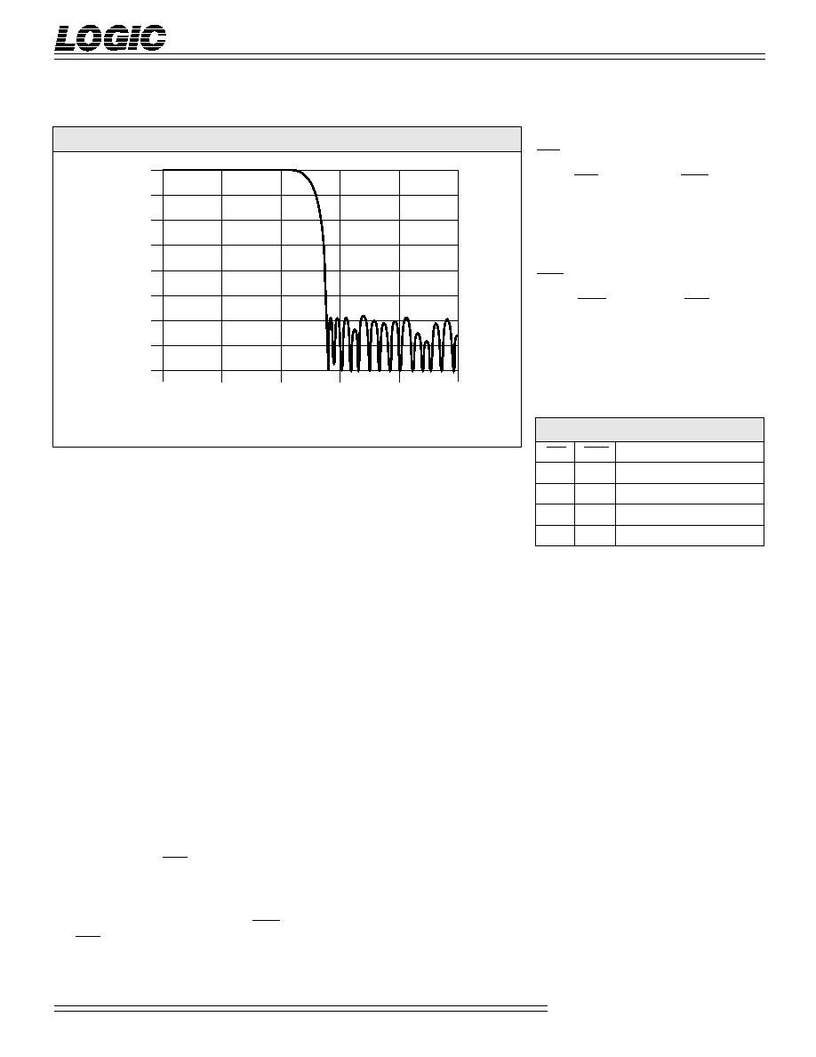
DC gain of the LF2242 is 1.0015
(0.0126 dB) in pass-through and
decimate modes and 0.5007 (≠3.004
dB) in interpolate mode. Passband
ripple does not exceed
±
0.02 dB from
0 to 0.22f
S
with stopband attenuation
greater than 59.4 dB from 0.28f
S
to
0.5f
S
(Nyquist frequency). The
response of the filter is ≠6 dB at 0.25f
S
.
Full compliance with CCIR Recom-
mendation 601 (≠12 dB at 0.25f
S
) can
be achieved by cascading two devices
serially.
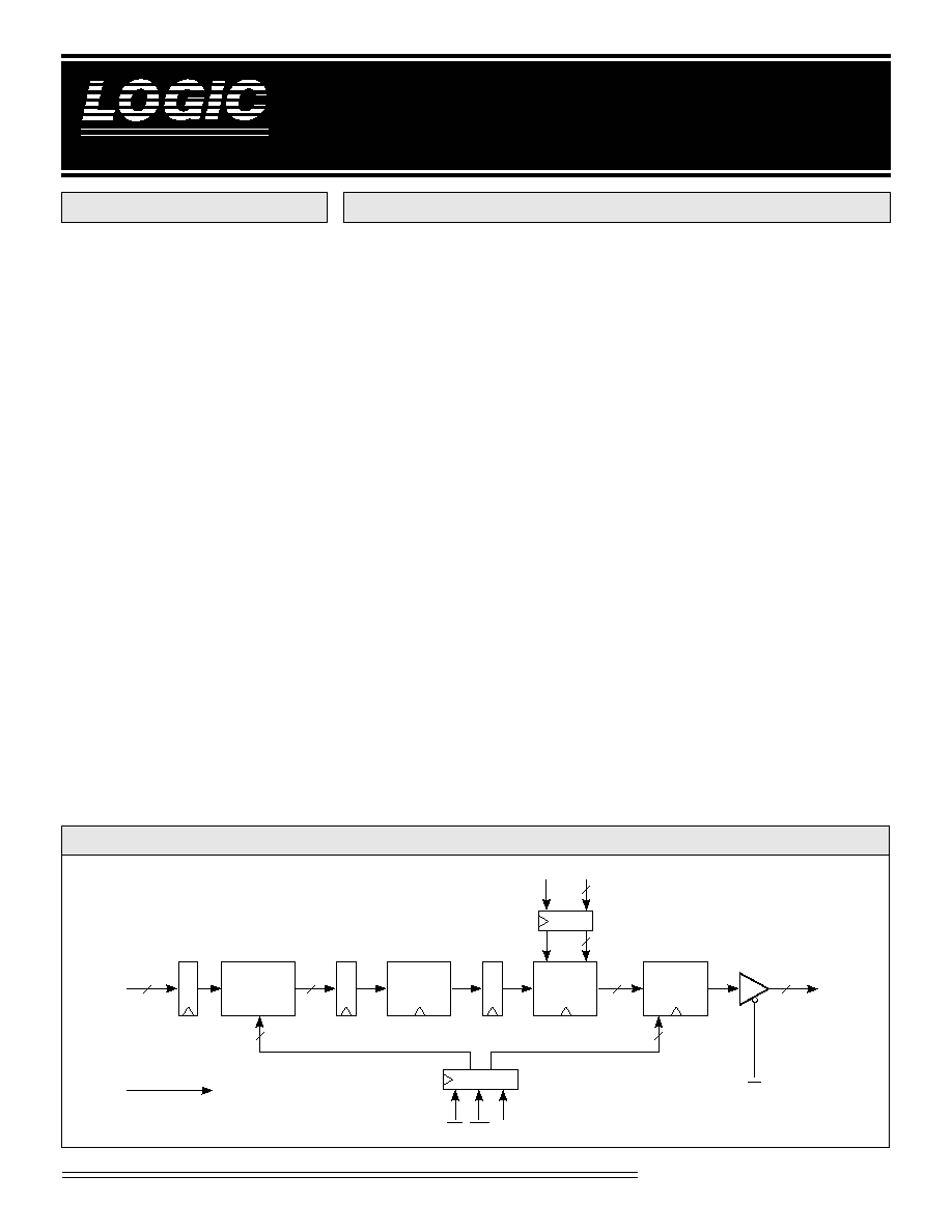
LF2242 B
LOCK
D
IAGRAM
OE
TO ALL REGISTERS
SI
11≠0
INTERPOLATION
CIRCUIT
55-TAP
FIR
FILTER
ROUND
AND LIMIT
CIRCUIT
DECIMATION
CIRCUIT
16
3
3
RND
2≠0
TCO
SO
15≠0
3
3
SYNC
INT DEC
CLK
16
12
12
DEVICES INCORPORATED
LF2242
12/16-bit Half-Band Interpolating/
Decimating Digital Filter
Video Imaging Products
2
08/16/2000≠LDS.2242-K
Controls
INT -- Interpolation Control
When INT is LOW and DEC is HIGH
(Table 1), the device internally forces
every other incoming data sample to
zero. This effectively halves the input
data rate and the output amplitude.
DEC -- Decimation Control
When DEC is LOW and INT is HIGH
(Table 1), the output register is strobed on
every other rising edge of CLK (driven at
half the clock rate), decimating the output
data stream.
F
IGURE
1.
F
REQUENCY
R
ESPONSE
OF
F
ILTER
SIGNAL DEFINITIONS
Power
V
CC
and GND
+5 V power supply. All pins must be
connected.
Clock
CLK -- Master Clock
The rising edge of CLK strobes all regis-
ters. All timing specifications are refer-
enced to the rising edge of CLK.
SYNC -- Synchronization Control
Incoming data is synchronized by hold-
ing SYNC HIGH on CLK
N
, and then by
bringing SYNC LOW on CLK
N+1
with
the first word of input data. SYNC is held
LOW until resynchronization is desired,
or it can be toggled at half the clock rate.
For interpolation (INT = LOW), input
data should be presented at the first ris-
ing edge of CLK for which SYNC is LOW
and then at every alternate rising edge of
CLK thereafter. SYNC is inactive if DEC
and INT are equal (pass-through mode).
Inputs
SI
11≠0
-- Data Input
12-bit two's complement data input
port. Data is latched into the register on
the rising edge of CLK. The LSB is SI
0
(Figure 2).
Outputs
SO
15-0
Data Output
The current 16-bit result is available on
the SO
15-0
outputs. The LF2242's limiter
ensures that a valid full-scale (7FFF
positive or 8000 negative) output will be
generated in the event of an internal
overflow. The LSB is SO
0
(Figure 2).
0
0.1
S
0.2
S
0.3
S
0.4
S
0.5
S
FREQUENCY (NORMALIZED)
0
≠10
≠20
≠30
≠40
≠50
≠60
≠70
≠80
GAIN (dB)
INT
DEC
MODE
0
0
Pass-through*
0
1
Interpolate
1
0
Decimate
1
1
Pass-through*
*Input and output registers run at full
clock rate
T
ABLE
1.
M
ODE
S
ELECTION
DEVICES INCORPORATED
LF2242
12/16-bit Half-Band Interpolating/
Decimating Digital Filter
Video Imaging Products
3
08/16/2000≠LDS.2242-K
RND
2-0
-- Rounding Control
The rounding control inputs set the posi-
tion of the effective LSB of the output data
by adding a rounding bit to the internal
bit position that is one below that speci-
fied by RND
2-0
. All bits below the effec-
tive LSB position are subsequently ze-
roed (Table 2).
TCO -- Two's Complement Format
Control
The TCO input determines the format of
the output data. When TCO is HIGH, the
output data is presented in two's comple-
ment format. When TCO is LOW, the
data is in inverted offset binary format
(all output bits are inverted except the
MSB -- the MSB is unchanged).
OE -- Output Enable
When the OE signal is LOW, the current
data in the output register is available on
the SO
15-0
pins. When OE is HIGH, the
outputs are in a high-impedance state.
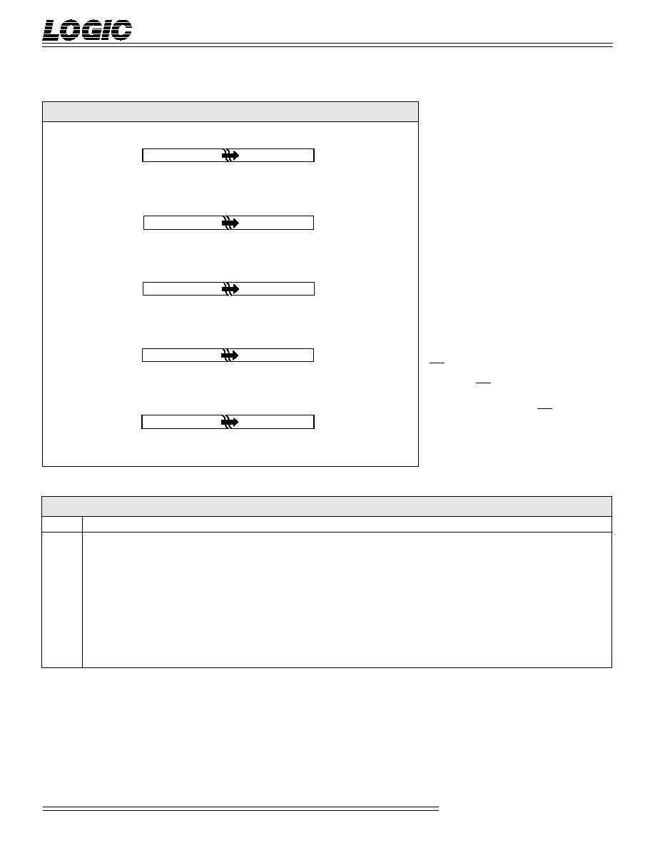
F
IGURE
2.
I
NPUT
AND
O
UTPUT
F
ORMATS
RND
2-0
SO
15
SO
14
SO
13
SO
12
∑ ∑ ∑
SO
8
SO
7
SO
6
SO
5
SO
4
SO
3
SO
2
SO
1
SO
0
000
X
X
X
X
∑ ∑ ∑
X
X
X
X
X
X
X
X
R
001
X
X
X
X
∑ ∑ ∑
X
X
X
X
X
X
X
R
0
010
X
X
X
X
∑ ∑ ∑
X
X
X
X
X
X
R
0
0
011
X
X
X
X
∑ ∑ ∑
X
X
X
X
X
R
0
0
0
100
X
X
X
X
∑ ∑ ∑
X
X
X
X
R
0
0
0
0
101
X
X
X
X
∑ ∑ ∑
X
X
X
R
0
0
0
0
0
110
X
X
X
X
∑ ∑ ∑
X
X
R
0
0
0
0
0
0
111
X
X
X
X
∑ ∑ ∑
X
R
0
0
0
0
0
0
0
'R' indicates the half-LSB rounded bit (effective LSB position)
T
ABLE
2.
R
OUNDING
F
ORMAT
Two's Complement Input Format
Two's Complement Output Format (TCO = 1, Non-interpolate)
Two's Complement Output Format (TCO = 1, Interpolate)
Inverted Offset Binary Output Format (TCO = 0, Non-interpolate)
Inverted Offset Binary Output Format (TCO = 0, Interpolate)
10
9
8
2
1
0
11
3
≠2
0
2
≠1
2
≠2
2
≠8
2
≠9
2
≠10
2
≠3
2
≠11
(Sign)
14 13 12
2
1
0
15
3
≠2
0
2
≠1
2
≠2
2
≠12
2
≠13
2
≠14
2
≠3
2
≠15
(Sign)
14 13 12
2
1
0
15
3
≠2
1
2
0
2
≠1
2
≠11
2
≠12
2
≠13
2
≠2
2
≠14
(Sign)
14 13 12
2
1
0
15
3
2
0
2
≠1
2
≠2
2
≠12
2
≠13
2
≠14
2
≠3
2
≠15
(Sign)
14 13 12
2
1
0
15
3
2
1
2
0
2
≠1
2
≠11
2
≠12
2
≠13
2
≠2
2
≠14
(Sign)
DEVICES INCORPORATED
LF2242
12/16-bit Half-Band Interpolating/
Decimating Digital Filter
Video Imaging Products
4
08/16/2000≠LDS.2242-K
Storage temperature ........................................................................................................... ≠65∞C to +150∞C
Operating ambient temperature ........................................................................................... ≠55∞C to +125∞C
V
CC
supply voltage with respect to ground ............................................................................ ≠0.5 V to +7.0 V
Input signal with respect to ground ............................................................................... ≠0.5 V to V
CC
+ 0.5 V
Signal applied to high impedance output ...................................................................... ≠0.5 V to V
CC
+ 0.5 V
Output current into low outputs ............................................................................................................. 25 mA
Latchup current ............................................................................................................................... > 400 mA
M
AXIMUM
R
ATINGS
Above which useful life may be impaired (Notes 1, 2, 3, 8)
O
PERATING
C
ONDITIONS
To meet specified electrical and switching characteristics
Mode
Temperature Range (Ambient)
Supply
Voltage
Active Operation, Commercial
0∞C to +70∞C
4.75 V
V
CC
5.25 V
Active Operation, Industrial
-40∞C to +85∞C
4.75 V
V
CC
5.25 V
Symbol
Parameter
Test Condition
Min
Typ
Max
Unit
V
OH
Output High Voltage
V
CC
= Min., I
OH
= ≠2.0 mA
2.4
V
V
OL
Output Low Voltage
V
CC
= Min., I
OL
= 4.0 mA
0.4
V
V
IH
Input High Voltage
2.0
V
CC
V
V
IL
Input Low Voltage
(Note 3)
0.0
0.8
V
I
IX
Input Current
Ground
V
IN
V
CC
(Note 12)
±
10
µA
I
OZ
Output Leakage Current
(Note 12)
±
10
µA
I
CC1
V
CC
Current, Dynamic
(Notes 5, 6)
80
mA
I
CC2
V
CC
Current, Quiescent
(Note 7)
10
mA
C
IN
Input Capacitance
T
A
= 25∞C, f = 1 MHz
10
pF
C
OUT
Output Capacitance
T
A
= 25∞C, f = 1 MHz
10
pF
E
LECTRICAL
C
HARACTERISTICS
Over Operating Conditions (Note 4)
DEVICES INCORPORATED
LF2242
12/16-bit Half-Band Interpolating/
Decimating Digital Filter
Video Imaging Products
5
08/16/2000≠LDS.2242-K
LF2242≠
33
25
Symbol
Parameter
Min
Max
Min
Max
t
CYC
Cycle Time
33
25
t
PW
Clock Pulse Width
10
10
t
S
Input Setup Time
10
8
t
H
Input Hold Time
0
0
t
D
Output Delay
20
16
t
DIS
Three-State Output Disable Delay (Note 11)
15
15
t
ENA
Three-State Output Enable Delay (Note 11)
15
15
SWITCHING CHARACTERISTICS
C
OMMERCIAL
O
PERATING
R
ANGE
(0∞C to +70∞C)
Notes 9, 10 (ns)
S
WITCHING
W
AVEFORMS
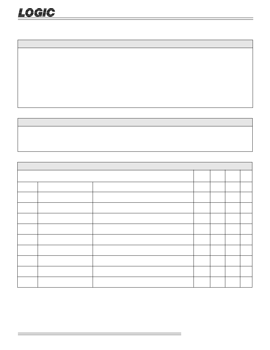
:
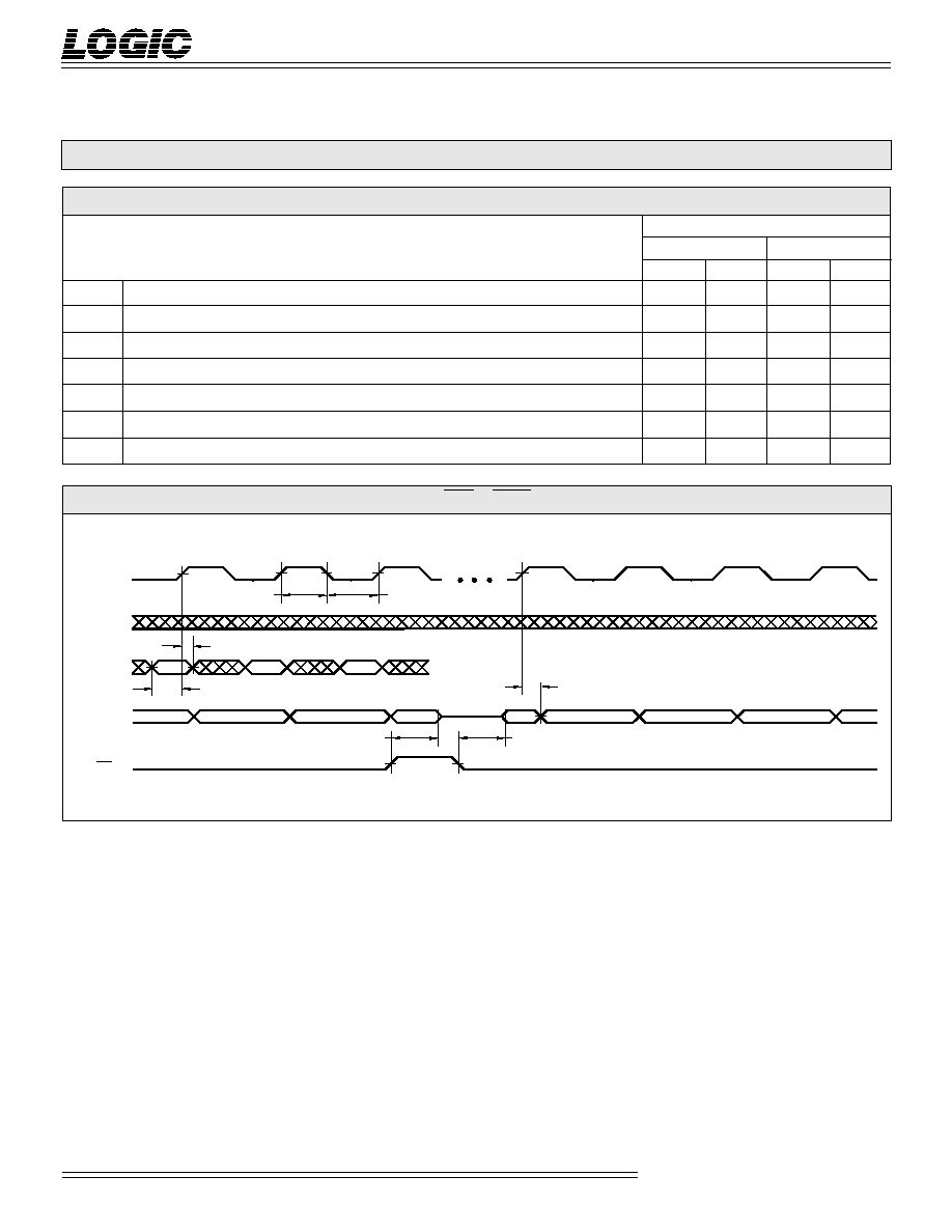
P
ASS
-T
HROUGH
M
ODE
(INT = DEC)
CLK
t
DIS
SI
11-0
SO
15-0
OE
N
t
S
t
PW
1
2
3
7
SYNC
N+1
N+2
t
H
8
9
10
HIGH IMPEDANCE
t
ENA
t
D
f(
N
)
f(
N+1
)
f(
N+2
)
t
PW