
DEVICES INCORPORATED
Video Imaging Products
1
LF3304
Dual Line Buffer/FIFO
08/16/2000≠LDS.3304-F
LF3304
Dual Line Buffer/FIFO
DEVICES INCORPORATED
u
u
u
u
u 100 MHz Data Rate for Video and
other High-Speed Applications
u
u
u
u
u One 24-bit, Two 12-bit, Three
8-bit Data Paths, or One Double
Depth 12-bit
u
u
u
u
u Dual Modes: Line Buffer or FIFO
u
u
u
u
u User-Programmable FIFO Flags
u
u
u
u
u User-Resettable Read and Write
Pointers
u
u
u
u
u Single 3.3 V Power Supply,
5 V Tolerant I/O
u
u
u
u
u 100-lead PQFP
FEATURES
DESCRIPTION
The LF3304 is a dual line buffer/
FIFO, designed to operate at HDTV
rates. The LF3304 will operate in
two distinct modes: Line Buffer and
FIFO. In these modes the two memo-
ries can operate independently or
with common control.
The LF3304 comprises two 12-bit 4K
memories configurable in a variety of
ways including: Two 12-bit 4K deep
line buffers (independent lengths),
Three 8-bit 4K deep line buffers
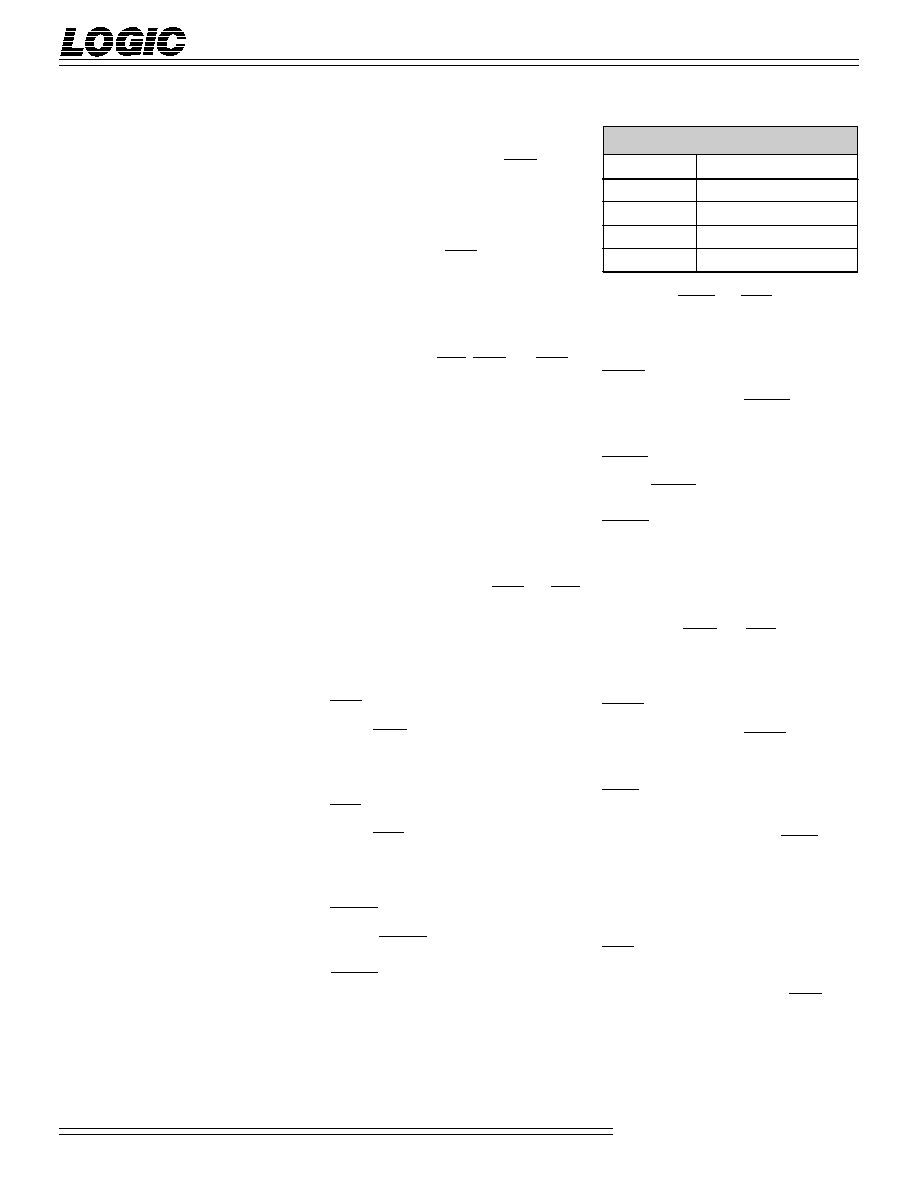
VARIABLE LENGTH RAM ARRAY B
4K x 12-bit
VARIABLE LENGTH RAM ARRAY A
4K x 12-bit
AIN
11-0
12
BIN
11-0
12
AOUT
11-0
12
BOUT
11-0
12
OEB
RAM ARRAY 2
CONTROL
LENGTH
11-0
WENB
RENB
RRB
RWB
RAM ARRAY 1
CONTROL
WENA
RENA
RRA
RWA
EFB
PAFB
FFB
PAEB
PAEA
FFA
EFA
PAFA
12
ADDRA
LDB
FLAG
GENERATOR
FLAG
GENERATOR
MASTER
CONTROL
MODE
1-0
2
WCLKA
RCLKA
WCLKB
RCLKB
LDA
ADDRB
OEA
LF3304 B
LOCK
D
IAGRAM
(common lengths), One 12-bit 8K
deep line buffer, or Two 12-bit 4K
FIFOs (independent operation).
In FIFO mode, independent Read
and Write Resets give the designer
control over the internal pointers
providing flexibility not commonly
found in ordinary FIFOs.
The LF3304 operatates at a maximum
data rate of 100 MHz and is available
in a 100-lead PQFP package.
DEVICES INCORPORATED
LF3304
Dual Line Buffer/FIFO
2
Video Imaging Products
08/16/2000≠LDS.3304-F
the data presented on LENGTH
11-0
is
loaded into the device on the active edge of
WCLKA in conjunction with LDA being
driven LOW. To set the length of RAM
Array B the data presented on
LENGTH
11-0
is loaded into the device
on the active edge of WCLKB in
conjunction with LDB being driven
LOW. If an equal length is desired for
both RAM Arrays, the data presented
on LENGTH
11-0
is loaded into the
device on the active edge of WCLK
(WCLKA and WCLKB tied together) in
conjuction with LDx (LDA and LDB
tied together) being driven LOW.
MODE
1-0
-- Mode Select
The mode select inputs determine the
operating mode of the LF3304 (Table 1) for
data being input on the next clock cycle.
When switching between modes, the
internal pipeline latencies of the device
must be observed. After switching
operating modes, either the user must
allow enough clock clycles to pass to flush
the internal RAM Array or RWx and RRx
must be driven LOW together before valid
data will appear on the outputs.
Controls
LDA -- RAM Array A Load
When LDA is LOW, data on
LENGTH
11-0
is latched in the length
register on the rising edge of xCLKA.
LDB -- RAM Array B Load
When LDB is LOW, data on
LENGTH
11-0
is latched in the length
register on the rising edge of xCLKB.
WENA -- Write Enable A
Driving WENA LOW places the device in
programmable delay mode and driving
WENA HIGH places RAM Array A in
recirculate mode (programmable circular
buffer). When in recirculate mode, the
write pointer position remains fixed while
data on AIN
11-0
is ignored. When
switching back from recirculate mode to
MODE
1-0
Mode Select
0 0
Dual Line Buffer
0 1
Cascaded Line Buffer
1 0
Dual FIFO
1 1
Reserved
delay mode, RWA and RRA should be
brought LOW to properly reset the Write
and Read pointers.
RENA -- Read Enable B
In Line Buffer mode, RENA must be
kept LOW.
WENB -- Write Enable B
Driving WENB LOW places the device in
programmable delay mode and driving
WENB HIGH places RAM Array B in
recirculate mode (programmable circular
buffer). When in recirculate mode, the
write pointer position remains fixed
while data on BIN
11-0
is ignored. When
switching back from recirculate mode to
delay mode, RWB and RRB should be
brought LOW to properly reset the Write
and Read pointers.
RENB -- Read Enable B
In Line Buffer mode, RENB must be
kept LOW.
RWA -- Reset Write A
The write address pointer is reset to the
first physical location when RWA is set
LOW. After power up, the LF3304
requires a Reset Write for initialization
because the write address pointer is not
defined at that time.
RRA -- Reset Read A
The read address pointer is reset to the
first physical location when RRA is set
LOW. After power up, the LF3304
requires a Reset Read for initialization
because the read address pointer is not
defined at that time.
LINE BUFFER MODE
SIGNAL DEFINITIONS
Power
V
CC
and GND
+3.3 V power supply. All pins must
be connected.
Clocks
WCLKA -- Write Clock A
WCLKA and RCLKA must be tied
together for RAM Array A to properly
operate as a Line Buffer. The rising edge
of xCLKA strobes all appropriate
enabled registers.
RCLKA -- Read Clock A
See WCLKA description.
WCLKB -- Write Clock B
WCLKB and RCLKB must be tied
together for RAM Array B to properly
operate as a Line Buffer. The rising
edge of xCLKB strobes all appropriate
enabled registers.
RCLKB -- Read Clock B
See WCLKB description.
Inputs
AIN
11-0
-- Data Input A
AIN
11-0
is the 12-bit registered data
input port.
BIN
11-0
-- Data Input B
BIN
11-0
is the 12-bit registered data
input port.
LENGTH
11-0
-- Line Buffer Length
The 12-bit value is used to specify the
length of each of the RAM Arrays. An
integer value ranging from 0 to 4095 is
used to select a delay ranging from 2 to
4097 clock cycles. The value placed on
LENGTH
11-0
is equal to the desired delay
minus 8. To set the length of RAM Array A
T
ABLE
1.
D
EVICE
C
ONFIGURATION
8
DEVICES INCORPORATED
Video Imaging Products
3
LF3304
Dual Line Buffer/FIFO
08/16/2000≠LDS.3304-F
RWB -- Reset Write B
See RWA Description.
RRB -- Reset Read B
See RRA description.
OEA -- Output Enable A
When OEA is LOW, AOUT
11-0
is
enabled for output. When OEA is
HIGH, AOUT
11-0
is placed in a high-
impedence state.
OEB -- Output Enable B
When OEB is LOW, BOUT
11-0
is
enabled for output. When OEB is
HIGH, BOUT
11-0
is placed in a high-
impedence state.
Outputs
AOUT
11-0
-- Data Output A
AOUT
11-0
is the 12-bit registered
data output port.
BOUT
11-0
-- Data Output B
BOUT
11-0
is the 12-bit registered
data output port.
FIFO MODE
SIGNAL DEFINITIONS
Power
V
CC
and GND
+3.3 V power supply. All pins must be
connected.
Clocks
WCLKA -- Write Clock A
Data present on AIN
11-0
is written
into the LF3304 on the rising edge of
WCLKA when the device is configured
for writing.
RCLKA -- Read Clock A
Data is read from the LF3304 and
presented on the output port (AOUT
11-0
)
after t
D
has elapsed from the rising
edge of RCLKA when the device is
configured for reading and the output
port is enabled. WCLKA and RCLKA
can be tied together and driven by the
same external clock or they may be
controlled by separate external clocks.
WCLKB -- Write Clock B
Data present on BIN
11-0
is written into
the LF3304 on the rising edge of
WCLKB when the device is configured
for writing.
RCLKB -- Read Clock B
Data is read from the LF3304 and
presented on the output port (BOUT
11-0
)
after t
D
has elapsed from the rising
edge of RCLKB when the device is
configured for reading and the output
port is enabled. WCLKB and RCLKB
can be tied together and driven by the
same external clock or they may be
controlled by separate external clocks.
Inputs
AIN
11-0
-- Data Input A
AIN
11-0
is the 12-bit registered data
input port.
BIN
11-0
-- Data Input B
BIN
11-0
is the 12-bit registered data
input port.
ADDRA -- Address A
If LDA is LOW, on the rising edge of
WCLKA data present on AIN
11-0
is
written into the PAFA or PAEA register
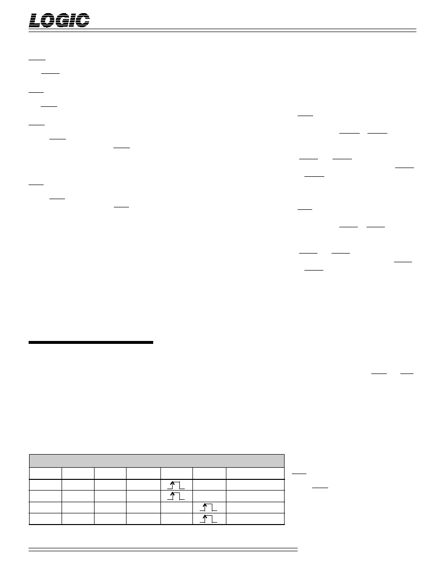
depending on ADDRA (see Table 2).
The LSB, AIN
0
, corresponds to the LSB
of PAFA and PAEA registers. The MSB,
AIN
11
, corresponds to the MSB of PAFA
and PAEA registers.
ADDRB -- Address B
If LDB is LOW, on the rising edge of
WCLKB data present on BIN
11-0
is
written into the PAFB or PAEB register
depending on ADDRB (see Table 2).
The LSB, BIN
0
, corresponds to the LSB
of PAFB and PAEB registers. The MSB,
BIN
11
, corresponds to the MSB of PAFB
and PAEB registers.
MODE
1-0
-- Mode Select
The mode select inputs determine the
operating mode of the LF3304 (Table 1) for
data being input on the next clock cycle.
When switching between modes, the
internal pipeline latencies of the device
must be observed. After switching
operating modes, either the user must
allow enough clock clycles to pass to flush
the internal RAM Array or RWx and RRx
must be driven LOW together before valid
data will appear on the outputs.
LENGTH -- Non-Flag Pins
In FIFO Mode, the unused LENGTH pins
(LENGTH
11
, LENGTH
10
, LENGTH
5
,
LENGTH
4
) must be tied LOW.
Controls
LDA -- RAM Array A Load
When LDA is LOW, data on AIN
11-0
is
latched in the LF3304 on the rising edge
of WCLKA.
T
ABLE
2.
L
OADING
P
ROGRAMMABLE
F
LAG
R
EGISTERS
ADDRA
ADDRB
LDA
LDB
WCLKA
WCLKB
Operation
0
x
0
x
x
PAEA Register
1
x
0
x
x
PAFA Register
x
0
x
0
x
PAEB Register
x
1
x
0
x
PAFB Register

DEVICES INCORPORATED
LF3304
Dual Line Buffer/FIFO
4
Video Imaging Products
08/16/2000≠LDS.3304-F
LDB -- RAM Array B Load
When LDB is LOW, data on BIN
11-0
is
latched in the LF3304 on the rising
edge of WCLKB.
WENA -- Write Enable A
If WENA is LOW, data on AIN
11-0
is
written to the device on the rising edge
of WCLKA. When RAM Array A is
full, WENA is ignored.
RENA -- Read Enable A
If RENA is LOW, data from RAM Array
A is read and presented on AOUT
11-0
after t
D
has elapsed from the rising
edge of RCLKA if the output port is
enabled. If RENA goes HIGH, the last
value loaded in the RAM Array A
output register will remain unchanged.
When RAM Array A is empty, RENA is
ignored.
WENB -- Write Enable B
If WENB is LOW, data on BIN
11-0
is
written to the device on the rising edgle
of WCLKB. When RAM Array B is full,
WENB is ignored.
RENB -- Read Enable B
If RENB is LOW, data from RAM Array
B is read and presented on BOUT
11-0
after tD has elapsed from the rising
edge of RCLKB if the output port is
enabled. If RENB goes HIGH, the last
value loaded in the RAM Array B
output register will remain unchanged.
When RAM Array B is empty, RENB is
ignored.
RWA -- Reset Write A
The write address pointer is reset to the
first physical location when RWA is set
LOW. After power up, the LF3304
requires a Reset Write for initialization
because the write address pointer is not
defined at that time.
RRA -- Reset Read A
The read address pointer is reset to the first
physical location when RRA is set LOW.
After power up, the LF3304 requires a Reset
Read for initialization because the read
address pointer is not defined at that time.
RWB -- Reset Write B
See RWA Description.
RRB -- Reset Read B
See RRA description.
OEA -- Output Enable A
When OEA is LOW, AOUT
11-0
is
enabled for output. When OEA is
HIGH, AOUT
11-0
is placed in a high-
impedence state. The flag outputs are
not affected by OEA.
OEB -- Output Enable B
When OEB is LOW, BOUT
11-0
is
enabled for output. When OEB is
HIGH, BOUT
11-0
is placed in a high-
impedence state. The flag outputs are
not affected by OEB.
Outputs
AOUT
11-0
-- Data Output A
AOUT
11-0
is the 12-bit registered data
output port.
BOUT
11-0
-- Data Output B
BOUT
11-0
is the 12-bit registered data
output port.
FFA -- Full Flag A
FFA goes LOW when RAM Array A is
full of data. When FFA is LOW, RAM
Array A can not be written to. The Full
Flag is synchronized to the rising edge
of WCLKA.
EFA -- Empty Flag A
EFA goes LOW when the read pointer is
equal to the write pointer, indicating that
RAM Array A is empty. When EFA is
LOW, read operations can not be
performed. The Empty Flag is synchro-
nized to the rising edge of RCLKA.
FFB -- Full Flag B
FFB goes LOW when RAM Array B is full
of data. When FFB is LOW, RAM Array B
can not be written to. The Full Flag is
synchronized to the rising edge of WCLKB.
EFB -- Empty Flag B
EFB goes LOW when the read pointer
is equal to the write pointer, indicating
that RAM Array B is empty. When EFB
is LOW, read operations can not be
performed. The Empty Flag is synchro-
nized to the rising edge of RCLKB.
PAFA -- Programmable Almost-Full Flag A
PAFA goes LOW when the write
pointer is (Full ≠ N) locations ahead of
the read pointer. N is the value stored
in the PAFA register and has no default
value. PAFA is synchronized to the
rising edge of WCLKA.
PAEA -- Programmable Almost-Empty Flag A
PAEA goes HIGH when the write
pointer is (N + 1) location ahead of the
read pointer. N is the value stored in
the PAEA register and has no default
value. PAEA is synchronized to the
rising edge of RCLKA.
PAFB -- Programmable Almost-Full Flag B
PAFB goes LOW
when
the write pointer
is (Full ≠ N) locations ahead of the read
pointer. N is the value stored in the
PAFB register and has no default value.
PAFB is synchronized to the rising
edge of WCLKB.
PAEB -- Programmable Almost-Empty Flag B
PAEB goes HIGH when the write
pointer is (N + 1) location ahead of the
read pointer. N is the value stored in
the PAEB register and has no default
value. PAEB is synchronized to the
rising edge of RCLKB.

DEVICES INCORPORATED
Video Imaging Products
5
LF3304
Dual Line Buffer/FIFO
08/16/2000≠LDS.3304-F
FIFO MODE
OPERATION
Initialization
Upon power-up, the LF3304 requires
the initialization of the internal read
and write address pointers. This
initialization sequence can be done
by either a Flag Enable Reset or a
Flag Disable Reset.
A Flag Enable Reset will force the
FIFO to operate in a `Flag Enabled'
mode. In this mode, writing will be
disabled when FFx is LOW and
reading is disabled when EFx is
LOW. Any `write beyond full' event
or `read beyond empty' event will be
disabled. Note: in an `empty' state,
the last data word read from the
FIFO is held on the output bus until
the next valid read cycle.
A Flag Disable Reset will force the
FIFO to operate in a `Flag Disabled'
mode. In this mode, the user is
allowed to write over previously un-
read data and read out previously
read data. Consequently, any
enabled write or read is valid thus
allowing the write and read pointers
to `wrap-around'. Note: due to the
nature of this mode, the flag status
should be disregarded. For example,
as the 4096th data word is written
into the FIFO, assuming that no
preceding read cycles have occured,
FFx will be driven LOW thus indicat-
ing a `full'state. While the FIFO is
still in this `full' state, the next
enabled write will access address
000H, thus writing over data that
has not yet been read out.
Flag Enable Reset
A Flag Enable Reset resets the read
and write pointers and enables the
flags to control the reading and
writing of data according to the Full
Flag and Empty Flag conditions. A
Flag Enable Reset occurs when the
following conditions are met:
1.
RWA/RWB must be LOW for at
least one WCLKA/WCLKB cycle.
2.
RRA/RRB must be LOW for at
least one RCLKA/RCLKB cycle.
3.
WENx and RENx must be HIGH
during the above two conditions
plus one addition write or read
cycle (which ever is longer).
The Flag Enable Reset condition can
be disabled if one of the two Flag
Disable Reset conditions are applied.
Flag Disable Reset
A Flag Disable Reset resets the read
and write pointers and disables the
flags from controlling the reading
and writing of data. A Flag Disable
Reset occurs when the following
conditions are met:
1.
RWA/RWB must be LOW for at
least one WCLKA/WCLKB cycle
while WENx is LOW.
2.
RRA/RRB must be LOW for at
least one RCLKA/RCLKB cycle
while RENx is LOW.
Configuration of Programmable Flags
In order to load a FIFO A Program-
mable Flag Register, a rising edge of
WCLKA, while WENA is LOW,
latches AIN11-0 into either the PAFA
or PAEA Register - depending on the
states of ADDRA and LDA (See
Table 2).
In order to load a FIFO B Program-
mable Flag Register, a rising edge of
WCLKB, while WENB is LOW,
latches BIN11-0 into either the PAFB
or PAEB Register - depending on the
states of ADDRB and LDB (See Table
2). See the Figure labeled "Program-
mable Flag Load Timing."