 | –≠–ª–µ–∫—Ç—Ä–æ–Ω–Ω—ã–π –∫–æ–º–ø–æ–Ω–µ–Ω—Ç: LF3320 | –°–∫–∞—á–∞—Ç—å:  PDF PDF  ZIP ZIP |
DEVICES INCORPORATED
Video Imaging Products
2-1
LF3320
Horizontal Digital Image Filter
08/16/2000≠LDS.3320-N
FEATURES
DESCRIPTION
The LF3320 filters digital images in the
horizontal dimension at real-time
video rates. The input and coefficient
data are both 12 bits and in two's
complement format. The output is also
in two's complement format and may
be rounded to 16 bits.
The LF3320 is designed to take
advantage of symmetric coefficient
sets. When symmetric coefficient sets
are used, the device can be configured
as a single 32-tap FIR filter or as two
separate 16-tap FIR filters.
When asymmetric coefficient sets are
used, the device can be configured as a
single 16-tap FIR filter or as two
separate 8-tap FIR filters. Multiple
LF3320s can be cascaded to create
larger filters.
Interleave/Decimation Registers (I/D
Registers) allow interleaved data to be
fed directly into the device and filtered
without separating the data into
individual data streams.
The LF3320 can handle a maximum of
sixteen data sets interleaved together.
The I/D Registers and on-chip accu-
mulators facilitate using decimation to
increase the number of filter taps.
Decimation of up to 16:1 is supported.
The LF3320 contains enough on-board
memory to store 256 coefficient sets.
Two separate LF Interfaces
TM
allow all
256 coefficient sets to be updated within
vertical blanking.
LF3320
Horizontal Digital Image Filter
DEVICES INCORPORATED
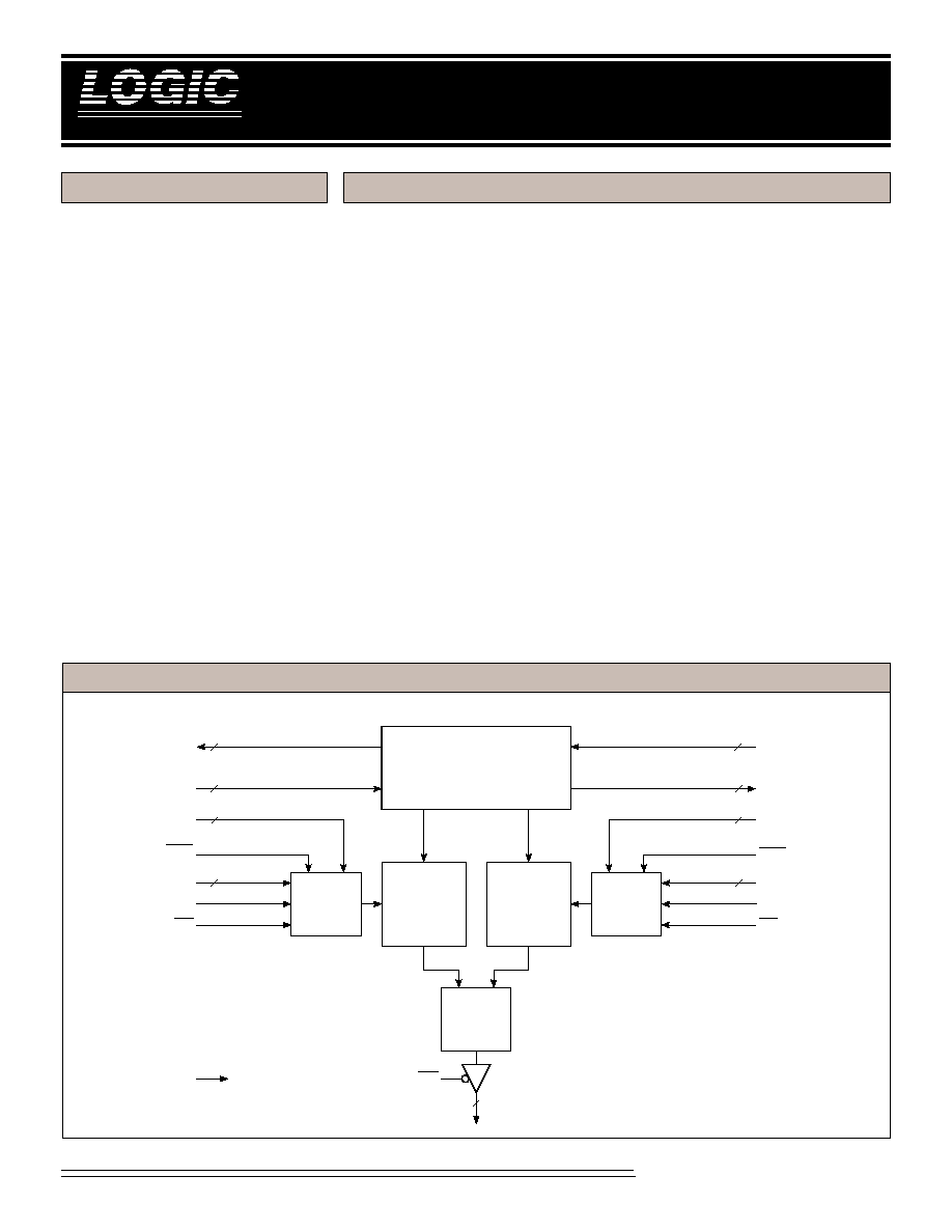
LF3320 B
LOCK
D
IAGRAM
83 MHz Data Rate
12-bit Data or Coefficients (Expand-
able to 24-bit)
32-Tap FIR Filter, Cascadable for
More Filter Taps
Over 49 K-bits of on-board Memory
LF Interface
TM
Allows All 256
Coefficient Sets to be Updated
Within Vertical Blanking
Various Operating Modes: Dual
Filter, Single Filter, Double Wide
Data or Coefficient, Matrix Multipli-
cation, and Accumulator Access.
Selectable 16-bit Data Output with
User-Defined Rounding and Limiting
Supports Interleaved Data Streams
Supports Decimation up to 16:1 for
Increasing Number of Filter Taps
3.3 Volt Supply
144 Lead PQFP
256
COEFFICIENT
SET
STORAGE
16-TAP
FILTER A
16-TAP
FILTER B
DIN
11-0
12
256
COEFFICIENT
SET
STORAGE
ROUT
11-0
12
12
12
ROUND
SELECT
LIMIT
CIRCUITRY
OED
CAA
7-0
CENA
8
CAB
7-0
CENB
8
COUT
11-0
RIN
11-0
DOUT
15-0
CFA
11-0
12
LDA
CFB
11-0
LDB
16
INTERLEAVE / DECIMATION
REGISTERS
12
CLK
PAUSEA
PAUSEB

DEVICES INCORPORATED
LF3320
Horizontal Digital Image Filter
2-2
08/16/2000≠LDS.3320-N
Video Imaging Products
F
IGURE
1.
LF3320 F
UNCTIONAL
B
LOCK
D
IAGRAM
DIN
11-0
32
12
ALU
AB
ALU
AB
ALU
AB
ALU
AB
ALU
AB
ALU
AB
ALU
AB
ALU
AB
13
Coef Bank 0
12
Coef Bank 1
12
Coef Bank 2
12
Coef Bank 3
12
13
13
13
13
13
13
13
25
25
25
25
25
25
25
25
27
27
CAA
7-0
CENA
ACCA
SHENA
CLK
1-16
1-16
1-16
1-16
1-16
1-16
1-16
1-16
1-16
1-16
1-16
1-16
1-16
1-16
1-16
Coef Bank 4
12
Coef Bank 5
12
Coef Bank 6
12
Coef Bank 7
12
32
ALU
AB
ALU
AB
ALU
AB
ALU
AB
ALU
AB
ALU
AB
ALU
AB
ALU
AB
13
12
12
12
12
13
13
13
13
13
13
13
25
25
25
25
25
25
25
25
27
27
ACCB
1-16
1-16
1-16
1-16
1-16
1-16
1-16
1-16
1-16
1-16
1-16
1-16
1-16
1-16
12
12
12
12
1-16
8
Coef Bank 15
Coef Bank 14
Coef Bank 13
Coef Bank 12
CAB
7-0
CENB
Coef Bank 11
Coef Bank 10
Coef Bank 9
Coef Bank 8
RIN
11-0
12
DOUT
15-0
16
OED
32
COUT
11-0
12
I
E O
R
DATA
REVERSAL
I
E O
S
DATA
REVERSAL
32
ACCM A
ACCM B
FILTER A
LF
INTERFACE
CFA
11-0
LDA
FILTER B
LF
INTERFACE
CFB
11-0
LDB
12
12
TXFRA
CONFIGURATION AND
CONTROL REGISTERS
8
16
16
"0"
"0"
TXFRB
SHENB
RSLB
RSLB OUT
15-0
RSLB OUT
15-12
SCALE
ROUND
SELECT
LIMIT
FILTER A
FILTER B
RSLA
3-0
RSLB
3-0
4
4
OEC
ROUT
3-0
4
ROUT
11-4
8
OEC
FILTER A I/D REGISTERS
FILTER B I/D REGISTERS
OUT
11-0
PAUSEA
PAUSEB
ROUND
SELECT
LIMIT

DEVICES INCORPORATED
Video Imaging Products
2-3
LF3320
Horizontal Digital Image Filter
08/16/2000≠LDS.3320-N
SIGNAL DEFINITIONS
Power
V
CC
and GND
+3.3 V power supply. All pins must be
connected.
Clock
CLK -- Master Clock
The rising edge of CLK strobes all
enabled registers.
Inputs
DIN
11-0
-- Data Input
DIN
11-0
is the 12-bit data input port to
Filter A. In Dual Filter Mode, DIN
11-0
can also be the 12-bit input port to
Filter B. Data is latched on the rising
edge of CLK.
RIN
11-0
-- Reverse Cascade Input
In Single Filter Mode, RIN
11-0
is the 12-
bit reverse cascade input port. This
port is connected to ROUT
11-0
of
another LF3320. In Dual Filter Mode,
RIN
11-0
can be the 12-bit input port to
Filter B. Data is latched on the rising
edge of CLK.
CFA
11-0
-- Coefficient A Input
CFA
11-0
is used to load data into the
Filter A coefficient banks (banks 0
through 7) and the configuration/
control registers. Data present on
CFA
11-0
is latched into the Filter A LF
Interface
TM
on the rising edge of CLK
when LDA is LOW (see the LF
Interface
TM
section for a full discus-
sion).
CAA
7-0
-- Coefficient Address A
CAA
7-0
determines which row of data
in coefficient banks 0 through 7 is fed
to the multipliers. CAA
7-0
is latched
into Coefficient Address Register A on
the rising edge of CLK when CENA is
LOW.
CFB
11-0
-- Coefficient B Input
CFB
11-0
is used to load data into the
Filter B coefficient banks (banks 8
through 15) and the configuration/
control registers. Data present on
CFB
11-0
is latched into the Filter B LF
Interface
TM
on the rising edge of CLK
when LDB is LOW (see the LF
Interface
TM
section for a full discussion).
CAB
7-0
-- Coefficient Address B
CAB
7-0
determines which row of data in
coefficient banks 8 through 15 is fed to the
multipliers. CAB
7-0
is latched into
Coefficient Address Register B on the
rising edge of CLK when CENB is LOW.
Outputs
DOUT
15-0
-- Data Output
DOUT
15-0
is the 16-bit registered data
output port for the overall filter (Single
Filter Mode) or Filter A (Dual Filter
Mode).
COUT
11-0
-- Cascade Output
In Single Filter Mode, COUT
11-0
is a
12-bit registered cascade output port.
COUT
11-0
should be connected to
DIN
11-0
of another LF3320. In Dual
Filter Mode, COUT
11-0
is a 12-bit
registered output port for the lower
twelve bits of the 16-bit Filter B output.
F
IGURE
2.
I
NPUT
F
ORMATS
11 10 9
2
1
0
≠2
11
(Sign)
2
10
2
9
2
2
2
1
2
0
11 10 9
2
1
0
≠2
0
(Sign)
2
≠1
2
≠2
2
≠9
2
≠10
2
≠11
Input Data
Coefficient Data
T
ABLE
1.
O
UTPUT
F
ORMATS
SLCT
4-0
S
15
S
14
S
13
∑ ∑ ∑
S
8
S
7
∑ ∑ ∑
S
2
S
1
S
0
00000
F
15
F
14
F
13
∑ ∑ ∑
F
8
F
7
∑ ∑ ∑
F
2
F
1
F
0
00001
F
16
F
15
F
14
∑ ∑ ∑
F
9
F
8
∑ ∑ ∑
F
3
F
2
F
1
00010
F
17
F
16
F
15
∑ ∑ ∑
F
10
F
9
∑ ∑ ∑
F
4
F
3
F
2
∑
∑
∑
∑
∑
∑
∑
∑
∑
∑
∑
∑
∑
∑
∑
∑
∑
∑
∑
∑
∑
∑
∑
∑
∑
∑
∑
01110
F
29
F
28
F
27
∑ ∑ ∑
F
22
F
21
∑ ∑ ∑
F
16
F
15
F
14
01111
F
30
F
29
F
28
∑ ∑ ∑
F
23
F
22
∑ ∑ ∑
F
17
F
16
F
15
10000
F
31
F
30
F
29
∑ ∑ ∑
F
24
F
23
∑ ∑ ∑
F
18
F
17
F
16
F
IGURE
3.
A
CCUMULATOR
O
UTPUT
F
ORMATS
31 30 29
2
1
0
≠2
20
(Sign)
2
19
2
18
2
≠9
2
≠10
2
≠11
31 30 29
2
1
0
≠2
20
(Sign)
2
19
2
18
2
≠9
2
≠10
2
≠11
Accumulator A Output
Accumulator B Output

DEVICES INCORPORATED
LF3320
Horizontal Digital Image Filter
2-4
08/16/2000≠LDS.3320-N
Video Imaging Products
ROUT
11-0
-- Reverse Cascade Output
In Single Filter Mode, ROUT
11-0
is a
12-bit registered cascade output port.
ROUT
11-0
on one device should be
connected to RIN
11-0
of another LF3320.
In Dual Filter Mode, ROUT
3-0
is a 4-bit
registered output port for the upper four
bits of the 16-bit Filter B output. In this
mode, ROUT
11-4
is disabled.
Controls
LDA -- Coefficient A Load
When LDA is LOW, data on CFA
11-0
is
latched into the Filter A LF Interface
TM
on the rising edge of CLK. When LDA is
HIGH, data is not loaded into the Filter
A LF Interface
TM
. When enabling the LF
Interface
TM
for data input, a HIGH to
LOW transition of LDA is required in
order for the input circuitry to function
properly. Therefore, LDA must be set
HIGH immediately after power up to
ensure proper operation of the input
circuitry (see the LF Interface
TM
section
for a full discussion).
CENA -- Coefficient Address Enable A
When CENA is LOW, data on CAA
7-0
is latched into Coefficient Address
Register A on the rising edge of CLK.
When CENA is HIGH, data on CAA
7-0
is not latched and the register's
contents will not be changed.
LDB -- Coefficient B Load
When LDB is LOW, data on CFB
11-0
is
latched into the Filter B LF Interface
TM
on the rising edge of CLK. When LDB is
HIGH, data is not loaded into the Filter
B LF Interface
TM
. When enabling the LF
Interface
TM
for data input, a HIGH to
LOW transition of LDB is required in
order for the input circuitry to function
properly. Therefore, LDB must be set
HIGH immediately after power up to
ensure proper operation of the input
circuitry (see the LF Interface
TM
section
for a full discussion).
CENB -- Coefficient Address Enable B
When CENB is LOW, data on CAB
7-0
is latched into Coefficient Address
Register B on the rising edge of CLK.
When CENB is HIGH, data on CAB
7-0
is not latched and the register's
contents will not be changed.
TXFRA -- Filter A LIFO Transfer
Control
TXFRA is used to change which LIFO
in the data reversal circuitry sends
data to the reverse data path and
which LIFO receives data from the
forward data path in Filter A. When
TXFRA goes LOW, the LIFO sending
data to the reverse data path becomes
the LIFO receiving data from the
forward data path, and the LIFO
receiving data from the forward data
path becomes the LIFO sending data to
the reverse data path. The device must
see a HIGH to LOW transition of
TXFRA in order to switch LIFOs.
TXFRA is latched on the rising edge of
CLK.
TXFRB -- Filter B LIFO Transfer
Control
TXFRB is used to change which LIFO
in the data reversal circuitry sends
data to the reverse data path and
which LIFO receives data from the
forward data path in Filter B. When
TXFRB goes LOW, the LIFO sending
data to the reverse data path becomes
the LIFO receiving data from the
forward data path, and the LIFO
receiving data from the forward data
path becomes the LIFO sending data to
the reverse data path. The device must
see a HIGH to LOW transition of
TXFRB in order to switch LIFOs.
TXFRB is latched on the rising edge of
CLK.
ACCA -- Accumulator A Control
When ACCA is HIGH, Accumulator A
is enabled for accumulation and the
Accumulator A Output Register is
disabled for loading. When ACCA is
LOW, no accumulation is performed
and the Accumulator A Output Register
is enabled for loading. ACCA is latched
on the rising edge of CLK.
ACCB -- Accumulator B Control
When ACCB is HIGH, Accumulator B
is enabled for accumulation and the
Accumulator B Output Register is
disabled for loading. When ACCB is
LOW, no accumulation is performed
and the Accumulator B Output Regis-
ter is enabled for loading. ACCB is
latched on the rising edge of CLK.
SHENA -- Filter A Shift Enable
In Dual Filter Mode, SHENA enables
or disables the loading of data into the
Input (DIN
11-0
) and Filter A I/D
Registers. When SHENA is LOW, data
is latched into the Input/Cascade
Registers and shifted through the I/D
Registers on the rising edge of CLK.
When SHENA is HIGH, data can not
be loaded into the Input/Cascade
Registers or shifted through the I/D
Registers and their contents will not be
changed.
In Single Filter Mode, SHENA also
enables or disables the loading of data
into the Reverse Cascade Input (RIN
11-
0
), Cascade Output (COUT
11-0
), Reverse
Cascade Output (ROUT
11-0
) and Filter B
I/D Registers. It is important to note
that in Single Filter Mode, both SHENA
and SHENB should be connected
together. Both must be active to enable
data loading in Single Filter Mode.
SHENA is latched on the rising edge of
CLK.
SHENB -- Filter B Shift Enable
In Dual Filter Mode, SHENB enables or
disables the loading of data into the
Reverse Cascade Input (RIN
11-0
),
Cascade Output (COUT
11-0
), Reverse
Cascade Output (ROUT
3-0
) and Filter B
I/D Registers. When SHENB is LOW,
data is latched into the Cascade Regis-
ters and shifted through the I/D

DEVICES INCORPORATED
Video Imaging Products
2-5
LF3320
Horizontal Digital Image Filter
08/16/2000≠LDS.3320-N
Registers on the rising edge of CLK.
When SHENB is HIGH, data can not be
loaded into the Cascade Registers or
shifted through the I/D Registers and
their contents will not be changed.
In Single Filter Mode, SHENB also
enables or disables the loading of data
into the Input (DIN
11-0
), Reverse
Cascade Output (ROUT
11-0
) and Filter
A I/D Registers. It is important to note
that in Single Filter Mode, both
SHENA and SHENB should be
connected together. Both must be
active to enable data loading in Single
Filter Mode. SHENB is latched on the
rising edge of CLK.
RSLA
3-0
-- Filter A Round/Select/Limit
Control
RSLA
3-0
determines which of the
sixteen user-programmable Round/
Select/Limit registers (RSL registers)
are used in the Filter A RSL circuitry.
A value of 0 on RSLA
3-0
selects RSL
register 0. A value of 1 selects RSL
register 1 and so on. RSLA
3-0
is
latched on the rising edge of CLK (see
the round, select, and limit sections for
a complete discussion).
RSLB
3-0
-- Filter B Round/Select/Limit
Control
RSLB
3-0
determines which of the sixteen
user-programmable RSL registers are
used in the Filter B RSL circuitry. A
value of 0 on RSLB
3-0
selects RSL
register 0. A value of 1 selects RSL
register 1 and so on. RSLB
3-0
is latched
on the rising edge of CLK (see the round,
select, and limit sections for a complete
discussion).
OED -- DOUT Output Enable
When OED is LOW, DOUT
15-0
is
enabled for output. When OED is
HIGH, DOUT
15-0
is placed in a high-
impedance state.
OEC -- COUT/ROUT Output Enable
When OEC is LOW, COUT
11-0
and
ROUT
3-0
are enabled for output. When
OEC is HIGH, COUT
11-0
and ROUT
3-0
are placed in a high-impedance state.
PAUSEA -- LF Interface
TM
Pause
When PAUSEA is HIGH, the Filter A
LF Interface
TM
loading sequence is
halted until PAUSEA is returned to a
LOW state. This effectively allows the
user to load coefficients and control
registers at a slower rate than the
master clock (see the LF Interface
TM
section for a full discussion).
PAUSEB -- LF Interface
TM
Pause
When PAUSEB is HIGH, the Filter B LF
Interface
TM
loading sequence is halted
until PAUSEB is returned to a LOW
state. This effectively allows the user
to load coefficients and control regis-
ters at a slower rate than the master
clock (see the LF Interface
TM
section for
a full discussion).
F
IGURE
4. S
INGLE
F
ILTER
M
ODE
DIN
11-0
I/D
REGISTERS
FILTER
A
RSL
CIRCUIT
FILTER
B
ROUT
11-0
COUT
11-0
DOUT
15-0
I/D
REGISTERS
12
12
12
16
RIN
11-0
12
DIN
11-0
I/D
REGISTERS
FILTER
A
FILTER
B
DOUT
15-0
I/D
REGISTERS
R.S.L.
CIRCUIT
R.S.L.
CIRCUIT
12
16
ROUT
3-0
/ COUT
11-0
16
RIN
11-0
12
F
IGURE
5. D
UAL
F
ILTER
M
ODE