
DEVICES INCORPORATED
Video Imaging Products
1
LF3330
Vertical Digital Image Filter
11/08/2001≠LDS.3330-M
u
u
u
u
u
83 MHz Data Rate
u
u
u
u
u 12-bit Data and Coefficients
u
u
u
u
u On-board Memory for 256
Coefficient Sets
u
u
u
u
u LF Interface
TM
Allows All 256
Coefficient Sets to be Updated
Within Vertical Blanking
u
u
u
u
u Selectable 16-bit Data Output with
User-Defined Rounding and
Limiting
u
u
u
u
u Seven 3K x 12-bit, Programmable
Two-Mode Line Buffers
u
u
u
u
u Separate Input Port for Odd and
Even Field Filtering
u
u
u
u
u 8 Filter Taps
u
u
u
u
u Cascadable for More Filter Taps
u
u
u
u
u Supports Interleaved Data Streams
u
u
u
u
u 3.3 Volt Power Supply
u
u
u
u
u 5 Volt Tolerant I/O
u
u
u
u
u 100 Lead PQFP
FEATURES
DESCRIPTION
The LF3330 filters digital images in
the vertical dimension at real-time
video rates. The input and coefficient
data are both 12 bits and in two's
complement format. The output is
also in two's complement format and
may be rounded to 16 bits.
The filter is an 8-tap FIR filter with all
required line buffers contained on-
chip. The line buffers can store video
lines with lengths from 4 to 3076
pixels.
Multiple LF3330s can be cascaded
together to create larger vertical
filters.
Due to the length of the line buffers,
interleaved data can be fed directly
into the device and filtered without
separating the data into individual
data streams. The number of inter-
leaved data sets that the device can
handle is limited only by the length of
the on-chip line buffers. If the inter-
leaved video line has 3076 data values
or less, the filter can handle it.
The LF3330 contains enough on-board
memory to store 256 coefficient sets.
The LF Interface
TM
allows all 256
coefficient sets to be updated within
vertical blanking.
Selectable 16-bit data output with
user-defined rounding and limiting
minimizes the constraints put on
coefficient sets for various filter
implementations.
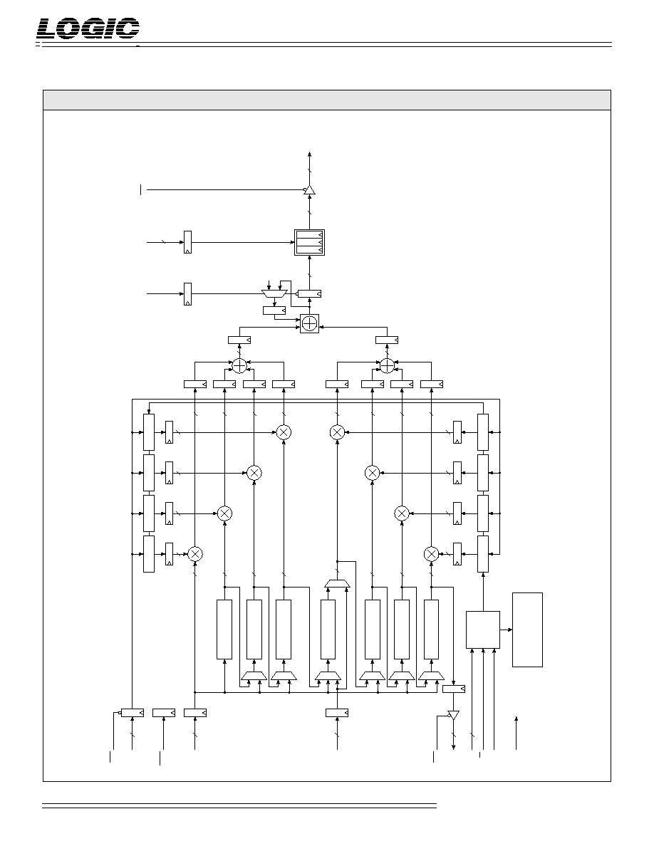
LF3330 B
LOCK
D
IAGRAM
LF3330
Vertical Digital Image Filter
DEVICES INCORPORATED
DIN
11-0
8-TAP VERTICAL FILTER
256 COEFFICIENT SET STORAGE
3K LINE BUFFER
12
3K LINE BUFFER
3K LINE BUFFER
3K LINE BUFFER
3K LINE BUFFER
3K LINE BUFFER
3K LINE BUFFER
ROUND
SELECT
LIMIT
CIRCUITRY
OED
16
DOUT
15-0
12
COUT
11-0
32
VB
11-0
12
OEC
DEVICES INCORPORATED
LF3330
Vertical Digital Image Filter
2
Video Imaging Products
11/08/2001≠LDS.3330-M
F
IGURE
1.
LF3330 F
UNCTIONAL
B
LOCK
D
IAGRAM
DIN
11-0
3K Line Buffer
32
12
12
12
12
12
12
12
12
3K Line Buffer
3K Line Buffer
3K Line Buffer
3K Line Buffer
3K Line Buffer
3K Line Buffer
24
24
24
24
24
24
24
24
26
26
12
12
12
12
12
12
12
12
12
ACC
SHEN
CLK
COUT
11-0
12
DOUT
15-0
OED
CA
7-0
CEN
8
LF
INTERFACE
CF
11-0
LD
12
CONFIGURATION AND
CONTROL REGISTERS
"0"
16
16
RSL
3-0
4
Coef Bank 7
Coef Bank 6
Coef Bank 5
Coef Bank 4
Coef Bank 0
Coef Bank 1
Coef Bank 2
Coef Bank 3
VB
11-0
12
PAUSE
OEC
ROUND
SELECT
LIMIT

DEVICES INCORPORATED
Video Imaging Products
3
LF3330
Vertical Digital Image Filter
11/08/2001≠LDS.3330-M
SIGNAL DEFINITIONS
Power
V
CC
and GND
+3.3 V power supply. All pins must be
connected.
Clock
CLK -- Master Clock
The rising edge of CLK strobes all
enabled registers
.
Inputs
DIN
11-0
-- Data Input
DIN
11-0
is the 12-bit registered data
input port. Data is latched on the rising
edge of CLK.
VB
11-0
-- Field Filtering Data Input
VB
11-0
is the 12-bit registered data
input port used only when implement-
ing Odd and Even Field Filtering (see
Functional Description section for a full
discussion). Data is latched on the
rising edge of CLK.
CF
11-0
-- Coefficient Input
CF
11-0
is used to load data into the
coefficient banks and configuration/
control registers. Data present on
CF
11-0
is latched into the LF Interface
TM
on the rising edge of CLK when LD is
LOW (see the LF Interface
TM
section for
a full discussion).
CA
7-0
-- Coefficient Address
CA
7-0
determines which row of data in
the coefficient banks is fed to the
multipliers. CA
7-0
is latched into the
Coefficient Address Register on the
rising edge of CLK when CEN is LOW.
Outputs
DOUT
15-0
-- Data Output
DOUT
15-0
is the 16-bit registered data
output port.
COUT
11-0
-- Cascade Data Output
COUT
11-0
is a 12-bit cascade
output port. COUT
11-0
on one
device should be connected to
DIN
11-0
of another LF3330.
Controls
LD -- Coefficient Load
When LD is LOW, data on CF
11-0
is latched into the LF Interface
TM
on the rising edge of CLK. When
LD is HIGH, data can not be
latched into the LF Interface
TM
.
When enabling the LF Interface
TM
for data input, a HIGH to LOW
transition of LD is required in
order for the input circuitry to
function properly. Therefore, LD
must be set HIGH immediately
after power up to ensure proper
operation of the input circuitry
(see the LF Interface
TM
section for
a full discussion).
PAUSE -- LF Interface
TM
Pause
When PAUSE is HIGH, the LF
Interface
TM
loading sequence is halted
until PAUSE is returned to a LOW
state. This effectively allows the user
to load coefficients and control
registers at a slower rate than the
master clock (see the LF Interface
TM
section for a full discussion).
CEN
-- Coefficient Address Enable
When CEN is LOW, data on CA
7-0
is
latched into the Coefficient Address
Register on the rising edge of CLK.
When CEN is HIGH, data on CA
7-0
is
not latched and the register's contents
will not be changed.
F
IGURE
2.
I
NPUT
F
ORMATS
11 10 9
2
1
0
≠2
11
(Sign)
2
10
2
9
2
2
2
1
2
0
11 10 9
2
1
0
≠2
0
(Sign)
2
≠1
2
≠2
2
≠9
2
≠10
2
≠11
Input Data
Coefficient Data
F
IGURE
3. A
CCUMULATOR
F
ORMAT
31 30 29
2
1
0
≠2
20
(Sign)
2
19
2
18
2
≠9
2
≠10
2
≠11
Accumulator Output
T
ABLE
1.
O
UTPUT
F
ORMATS
SLCT
4-0
S
15
S
14
S
13
∑ ∑ ∑
S
8
S
7
∑ ∑ ∑
S
2
S
1
S
0
00000
F
15
F
14
F
13
∑ ∑ ∑
F
8
F
7
∑ ∑ ∑
F
2
F
1
F
0
00001
F
16
F
15
F
14
∑ ∑ ∑
F
9
F
8
∑ ∑ ∑
F
3
F
2
F
1
00010
F
17
F
16
F
15
∑ ∑ ∑
F
10
F
9
∑ ∑ ∑
F
4
F
3
F
2
∑
∑
∑
∑
∑
∑
∑
∑
∑
∑
∑
∑
∑
∑
∑
∑
∑
∑
∑
∑
∑
∑
∑
∑
∑
∑
∑
01110
F
29
F
28
F
27
∑ ∑ ∑
F
22
F
21
∑ ∑ ∑
F
16
F
15
F
14
01111
F
30
F
29
F
28
∑ ∑ ∑
F
23
F
22
∑ ∑ ∑
F
17
F
16
F
15
10000
F
31
F
30
F
29
∑ ∑ ∑
F
24
F
23
∑ ∑ ∑
F
18
F
17
F
16
DEVICES INCORPORATED
LF3330
Vertical Digital Image Filter
4
Video Imaging Products
11/08/2001≠LDS.3330-M
ACC -- Accumulator Control
When ACC is HIGH, the accumulator
is enabled for accumulation and the
accumulator output register is
disabled for loading. When ACC is
LOW, no accumulation is performed
and the accumulator output register
is enabled for loading. ACC is
latched on the rising edge of CLK.
SHEN -- Shift Enable
SHEN enables or disables the
loading of data into the input/
cascade registers and the line
buffers. When SHEN is LOW, data
is loaded into the input/cascade
registers and shifted through the
line buffers on the rising edge of
CLK. When SHEN is HIGH, data
can not be loaded into the input/
cascade registers or shifted through
the line buffers and their contents
will not be changed.
RSL
3-0
-- Round/Select/Limit Control
RSL
3-0
determines which of the
sixteen user-programmable round/
select/limit registers are used in the
round/select/limit circuitry. A
value of 0 on RSL
3-0
selects round/
select/limit register 0. A value of 1
selects round/select/limit register 1
and so on. RSL
3-0
is latched on the
rising edge of CLK (see the round,
select, and limit sections for a
complete discussion).
OED -- DOUT Output Enable
When OED is LOW, DOUT
15-0
is
enabled for output. When OED is
HIGH, DOUT
15-0
is placed in a
high-impedance state.
OEC -- COUT Output Enable
When OEC is LOW, COUT
15-0
is
enabled for output. When OEC is
HIGH, COUT
15-0
is placed in a high-
impedance state.
BITS
FUNCTION
DESCRIPTION
0
Limit Enable
0 : Limiting Disabled
1 : Limiting Enabled
11-1
Reserved
Must be set to "0"
T
ABLE
4.
C
ONFIGURATION
R
EGISTER
2 ≠ A
DDRESS
202H
BITS
FUNCTION
DESCRIPTION
0
Cascade Mode
0 : First Device
1 : Cascaded Device
11-1
Reserved
Must be set to "0"
T
ABLE
5.
C
ONFIGURATION
R
EGISTER
3 ≠ A
DDRESS
203H
BITS
FUNCTION
DESCRIPTION
11-0
Line Buffer Length
See Line Buffer Description Section
T
ABLE
2.
C
ONFIGURATION
R
EGISTER
0 ≠ A
DDRESS
200H
BITS
FUNCTION
DESCRIPTION
0
Line Buffer Mode
0 : Delay Mode
1 : Recirculate Mode
1
Line Buffer Load
0 : Normal Load
1 : Parallel Load
2
Odd and Even Field
0 : VB Port Disabled
Filtering Port Enable
1 : VB Port Enabled
3
Odd and Even Field
0 : VB Line Buffer Disabled
Filtering Line Buffer Enable
1 : VB Line Buffer Enabled
11-4
Reserved
Must be set to "0"
T
ABLE
3.
C
ONFIGURATION
R
EGISTER
1 ≠ A
DDRESS
201H
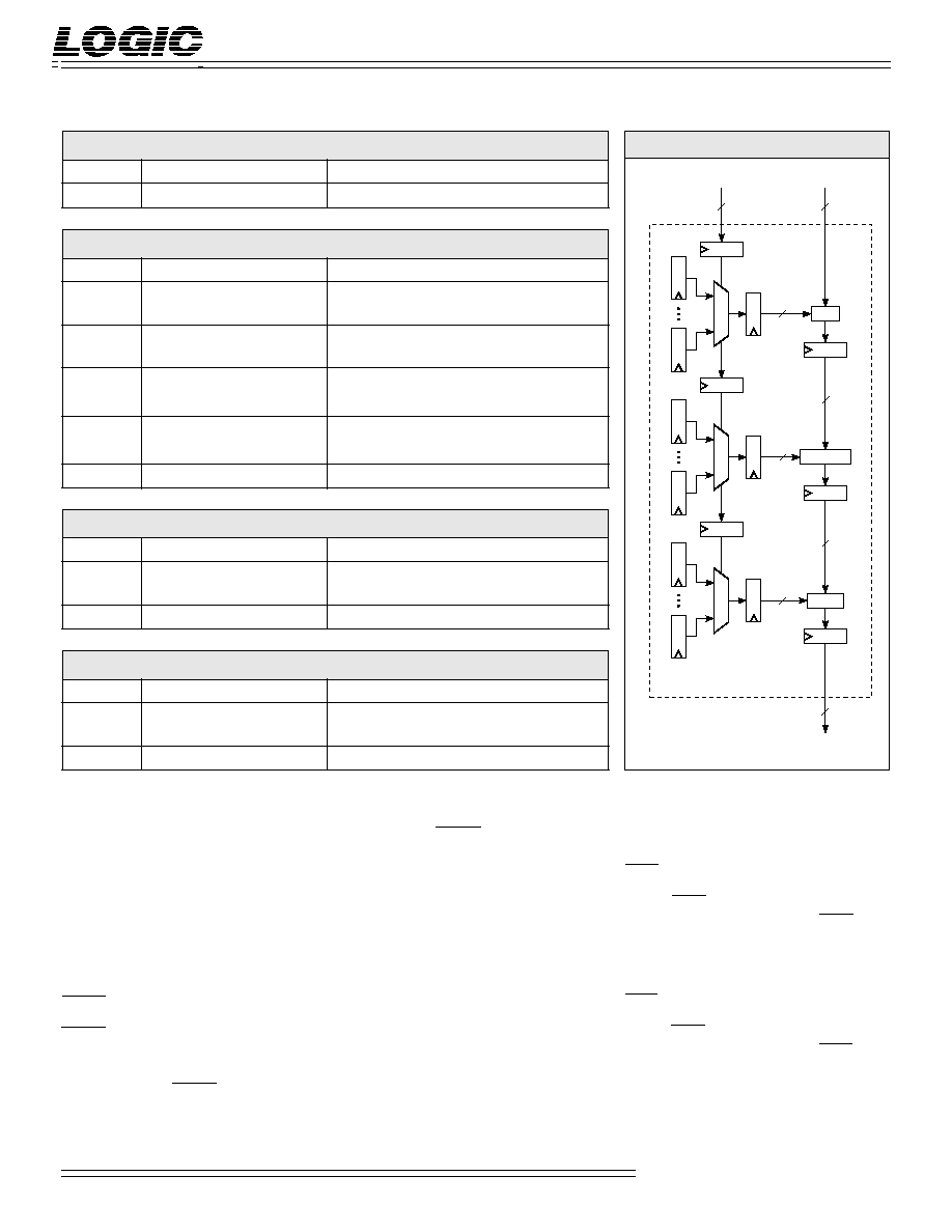
F
IGURE
4. RSL C
IRCUITRY
R0
R15
32
L0
L15
32
4
RSL
3-0
RND
LIMIT
32
16
16
RSL CIRCUITRY
DATA IN
32
DATA OUT
S0
S15
5
SELECT

DEVICES INCORPORATED
Video Imaging Products
5
LF3330
Vertical Digital Image Filter
11/08/2001≠LDS.3330-M
F
IGURE
5.
M
ULTIPLE
LF3330
S
C
ASCADED
T
OGETHER
DIN
LINE BUFFERS
VERTICAL FILTER
RSL
CIRCUIT
COUT
DIN
RSL
CIRCUIT
COUT
COUT
RSL
CIRCUIT
LF3330
DIN
DIN
DATA OUT
29 TAP RESULT
LF3330
LF3330
LF3330
12
RSL
CIRCUIT
LINE BUFFERS
LINE BUFFERS
LINE BUFFERS
VERTICAL FILTER
VERTICAL FILTER
VERTICAL FILTER
LF3347
RSL
CIRCUIT
16
25
25
FUNCTIONAL DESCRIPTION
Line Buffers
The maximum delay length of each line
buffer is 3076 cycles and the minimum
is 4 cycles. Configuration Register 0
(CR
0
) determines the delay length of
the line buffers. The line buffer length
is equal to the value of CR
0
plus 4. A
value of 0 for CR
0
sets the line buffer
length to 4. A value of 3072 for CR
0
sets the line buffer length to 3076. Any
values for CR
0
greater than 3072 are not
valid.
The line buffers have two modes of
operation: delay mode and recirculate
mode. Bit 0 of Configuration Register 1
determines which mode the line buffers
are in. In delay mode, the data input to
the line buffer is delayed by an amount
determined by CR
0
. In recirculate
mode, the output of the line buffer is
routed back to the input of the line
buffer allowing the line buffer contents
to be read multiple times.
Bit 1 of Configuration Register 1 allows
the line buffers to be loaded in parallel.
When Bit 1 is "1", the input register
(DIN
11-0
) loads all seven line buffers in
parallel. This allows all the line buffers
to be preloaded with data in the
amount of time it normally takes to
load a single line buffer.
Odd and Even Field Filtering
The LF3330 is capable of odd and even
field filtering. Bit 2 of Configuration
Register 1 enables the VB Data Input
port required for odd and even field
filtering. Bit 3 of the same configura-
tion register enables the line buffer in
the VB Data path. Line buffer length is
set to the length written to Configura-
tion Register 0. If line buffer parallel
load is enabled and odd and even field
filtering is enabled, the data for the VB
line buffer comes from the VB Data
Input port.
Interleaved Data
The LF3330 is capable of handling
interleaved data. The number of data
sets it can handle is determined by the
number of data values contained in a
video line. If the interleaved video line
has 3076 data values or less, the LF3330
can handle it no matter how many data
sets are interleaved together.
Cascading
A cascade port is provided to allow
cascading of multiple devices for
more filter taps (see Figure 5).
COUT
11-0
of one device should be
connected to DIN
11-0
of another
device. As many LF3330s as desired
may be cascaded together. How-
ever, the outputs of the LF3330s
must be added together with exter-
nal adders.
The first line buffer on a cascaded
device must have its length short-
ened by two delays. This is to
account for the added delays of the
input register on the device and the
cascade output register from the
previous LF3330. If Bit 0 of Con-
figuration Register 3 is set to "1",
the length of the first line buffer will
be reduced by two. This will make
its effective length the same as the
other line buffers on the device. If
Bit 0 of Configuration Register 3 is
set to "0", the length of the first line
buffer will be the same as the other
line buffers. When cascading
devices, the first LF3330 should
have Bit 0 of Configuration Register