
DEVICES INCORPORATED
Video Imaging Products
1
LF48212
12 x 12-bit Alpha Mixer
08/16/2000≠LDS.48212-F
u
u
u
u
u 50 MHz Data and Computation
Rate
u
u
u
u
u Two's Complement or Unsigned
Operands
u
u
u
u
u On-board Programmable Delay
Stages
u
u
u
u
u Programmable Output Rounding
u
u
u
u
u Replaces Harris HSP48212
u
u
u
u
u Package Styles Available:
∑ 68-pin PLCC, J-Lead
∑ 64-pin PQFP
FEATURES
DESCRIPTION
LF48212
12 x 12-bit Alpha Mixer
DEVICES INCORPORATED
The LF48212 is a high-speed video
alpha mixer capable of mixing video
signals at real-time video rates. It
takes two 12-bit video signals and
mixes them together using an alpha
mix factor. Alpha determines the
weighting that each video signal
receives during the mix operation.
The input video data can be in either
unsigned or two's complement
format, but both inputs must be in the
same format. Independently con-
trolled programmable delay stages are
provided for the input and control
signals to allow for allignment of
input data if necessary. The delay
stages can be programmed to have
from 0 to 7 delays. The 13-bit output
of the alpha mixer is registered with
three-state drivers and may be
rounded to 8, 10, 12, or 13-bits.
LF48212 B
LOCK
D
IAGRAM
DINA
11-0
11-0
DINB
11-0
FORMAT
FORMAT
0-7
1.0 ≠
0-7
0-7
ADJUST
FORMAT
DOUT
12-0
0-7
0-7
TC
RND
1-0
DELAY CONTROL
REGISTER
BYPASS
DEL
LD
CLK
MIXEN
OE
NOTE: NUMBERS IN REGISTERS INDICATE
NUMBER OF PIPELINE DELAYS.
12
12
12
13
2
15
4
4

DEVICES INCORPORATED
LF48212
12 x 12-bit Alpha Mixer
2
Video Imaging Products
08/16/2000≠LDS.48212-F
SIGNAL DEFINITIONS
Power
V
CC
and GND
+5 V power supply. All pins must be
connected.
Clock
CLK -- Master Clock
The rising edge of CLK strobes all
enabled registers except for the Delay
Control Register.
Inputs
DINA
11-0
-- Pixel Data Input A
DINA
11-0
is one of the 12-bit regis-
tered data input ports. Data is latched
on the rising edge of CLK.
DINB
11-0
-- Pixel Data Input B
DINB
11-0
is the other 12-bit registered
data input port. Data is latched on the
rising edge of CLK.
11-0
-- Alpha Mix Input
11-0
determines the weighting
applied to the data input signals
before being mixed together. DINA
11-0
and DINB
11-0
receive weightings of
and 1.0 ≠
respectively.
11-0
is
unsigned and restricted to the range of
0 to 1.0. Figure 1 shows the data
format for
11-0
. If a value greater
than 1.0 is latched into the Alpha Mix
Input, internal circuitry will force the
value to be equal to 1.0. Data is
latched on the rising edge of CLK.
DEL -- Delay Data Input
DEL is used to load the Delay Control
Register. The Delay Control Register
contains a 15-bit value which deter-
mines the number of delay stages
added to the input and control signals.
The 15-bit data value is loaded serially
into the Delay Control Register using
DEL and LD. Data present on DEL is
latched on the rising edge of LD.
F
IGURE
1.
A
LPHA
M
IX
I
NPUT
F
ORMAT
11 10 9
6
5
4
8
7
3
2
1
0
2
0
2
≠1
2
≠2
2
≠5
2
≠6
2
≠7
2
≠3
2
≠4
2
≠8
2
≠9
2
≠10
2
≠11
Outputs
DOUT
12-0
-- Data Output
DOUT
12-0
is the 13-bit registered data
output port.
Controls
TC -- Data Format Control
TC determines if the input data is in
unsigned or two's complement
format. If TC is LOW, the data is in
two's complement format. If TC is
HIGH, the data is in unsigned format.
Data present on TC is latched on the
rising edge of CLK. TC only affects
the data that is being latched into the
LF48212. Changing TC does not affect
internal data already in the pipeline.
MIXEN -- Alpha Mix Input Enable
When HIGH, data on
11-0
is latched
into the LF48212 on the rising edge of
CLK. When LOW, data on
11-0
is not
latched and the last value loaded is
held as the alpha mix value.
LD -- Load Strobe
The rising edge of LD latches the data
on DEL into the Delay Control Register.
BYPASS -- Bypass Delay Stage Control
The BYPASS control is used to bypass
the internal programmable delay
stages. When BYPASS is set HIGH,
the Delay Control Register will
automatically be loaded with a "0".
This will set the number of program-
mable delay stages to zero for all
input and control signals. When
BYPASS is LOW, the desired number
of delay stages can be set by loading
RND
1-0
ROUNDING FORMAT
00
Round to 8-bits
01
Round to 10-bits
10
Round to 12-bits
11
Round to 13-bits
T
ABLE
1.
O
UTPUT
R
OUNDING
the Delay Control Register with the
appropriate value. Note that this
signal is not intended to change
during active operation of the
LF48212.
RND
1-0
-- Output Rounding Control
RND
1-0
determines how the output of
the LF48212 is rounded. The output
may be rounded to 8, 10, 12, or 13-bits.
Table 1 lists the different rounding
possibilities and the associated value
for RND
1-0
. Rounding is accom-
plished by adding a "1" to the bit to
the right of what will become the least
significant bit. Then the bit that had
the "1" added to it and all bits to the
right of it are set to "0". Data present
on RND
1-0
is latched on the rising
edge of CLK. When RND
1-0
is latched
in, it only applies to the video input
data latched in at the same time.
Changing RND
1-0
does not affect the
rounding format for internal data
already in the pipeline.
OE -- Output Enable
When OE is LOW, DOUT
12-0
is
enabled for output. When OE is
HIGH, DOUT
12-0
is placed in a high-
impedance state.
DEVICES INCORPORATED
Video Imaging Products
3
LF48212
12 x 12-bit Alpha Mixer
08/16/2000≠LDS.48212-F
FUNCTIONAL DESCRIPTION
The two video signals to be mixed
together are input to the LF48212
using DINA
11-0
and DINB
11-0
. Data
present on DINA
11-0
and DINB
11-0
is
latched on the rising edge of CLK.
The input data may be in either
unsigned or two's complement
format, but both inputs must be in the
same format. TC determines the
format of the input data. When TC is
HIGH, the input data is in unsigned
format. When TC is LOW, the input
data is in two's complement format.
TC is latched on the rising edge of
CLK and only affects the input data
latched in at the same time. The data
already in the pipeline is not affected
when TC changes.
DINA
11-0
and DINB
11-0
are mixed
together using an alpha mix factor
(
11-0
) as defined by the equation
listed in Figure 2.
11-0
is unsigned
and restricted to the range of 0 to 1.0.
MIXEN controls the loading of alpha
mix data. When MIXEN is HIGH,
data present on
11-0
is latched on the
rising edge of CLK. When MIXEN is
LOW, data present on
11-0
is not
latched and the last value loaded is
held as the alpha mix value.
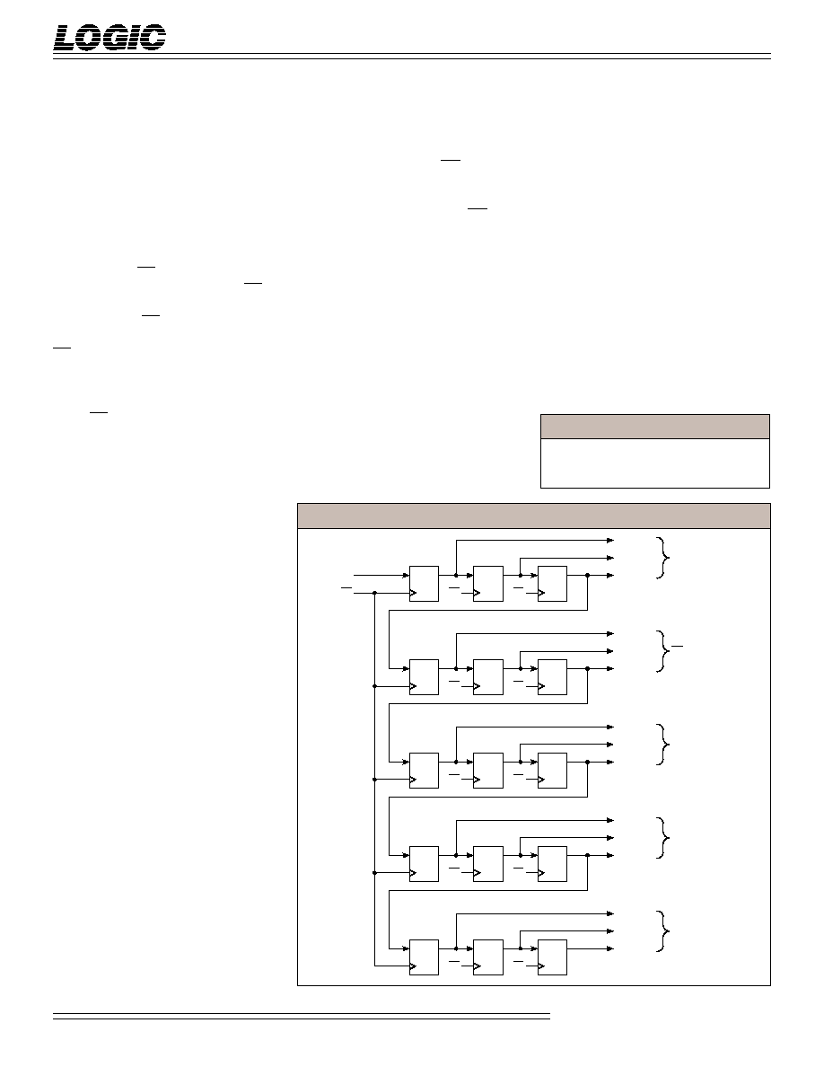
It is possible to add extra delay stages
to the input data and control signals
by using the programmable delay
stages. The 15-bit value (DELAY
14-0
)
stored in the Delay Control Register
determines the number of delay stages
added. DELAY
14-0
is divided into 5
groups of 3-bits each. Each 3-bit
group contains the delay information
for one of the input data or control
signals. Figure 3 shows the block
diagram of the Delay Control Register
as well as a list of the input data and
control signals that may be delayed
and the DELAY signals that control
them. The delay length can be pro-
grammed to be from 0 to 7 stages. The
delay length is set by loading the
binary equivalent of the desired delay
length into the appropriate 3-bit
group. For example, to add four extra
delay stages to DINB
11-0
, DELAY
5-3
should be set to "100". DELAY
14-0
is
loaded serially into the Delay Control
Register using DEL and LD. DELAY
0
is the first value loaded and DELAY
14
is the last. Data present on DEL is
latched on the rising edge of LD.
BYPASS is used to disable the pro-
grammable delay stages. When
BYPASS is HIGH, the Delay Control
Register is automatically loaded with
a "0". This sets all programmable
delay stages to a length of zero. When
BYPASS is LOW, the Delay Control
Register may be loaded to set the
desired number of delay stages. Note
that BYPASS is not intended to change
during active operation of the
LF48212.
The Adjust stage of the LF48212 is
used to maximize the precision of the
output data. Since
can never be
larger than 1.0, the most significant bit
of the internal summer output is not
needed. The Adjust stage takes the
output of the internal summer and left
shifts the data one bit position. This
removes the MSB of the internal
summer output and provides one
more bit of precision for the output
data.
The output data of the LF48212 may
be rounded to 8, 10, 12, or 13-bits.
RND
1-0
determines how the output is
rounded (See Table 1). RND
1-0
is
latched on the rising edge of CLK and
only affects the input data latched in
at the same time. The data already in
the pipeline is not affected when
RND
1-0
changes.
F
IGURE
3.
D
ELAY
C
ONTROL
R
EGISTER
B
LOCK
D
IAGRAM
DEL
LD
D
Q
D
Q
D
Q
DELAY
14
DELAY
13
DELAY
12
LD
LD
D
Q
D
Q
D
Q
DELAY
11
DELAY
10
DELAY
9
LD
LD
D
Q
D
Q
D
Q
DELAY
8
DELAY
7
DELAY
6
LD
LD
D
Q
D
Q
D
Q
DELAY
5
DELAY
4
DELAY
3
LD
LD
D
Q
D
Q
D
Q
DELAY
2
DELAY
1
DELAY
0
LD
LD
RND
1-0
DELAY
TC DELAY
11-0
DELAY
DINB
11-0
DELAY
DINA
11-0
DELAY
F
IGURE
2.
O
UTPUT
E
QUATION
OUTPUT =
(DINA) + (1 ≠
)DINB

DEVICES INCORPORATED
LF48212
12 x 12-bit Alpha Mixer
4
Video Imaging Products
08/16/2000≠LDS.48212-F
O
PERATING
C
ONDITIONS
To meet specified electrical and switching characteristics
Mode
Temperature Range (Ambient)
Supply
Voltage
Active Operation, Commercial
0∞C to +70∞C
4.75 V
V
CC
5.25 V
Storage temperature ........................................................................................................... ≠65∞C to +150∞C
Operating ambient temperature ........................................................................................... ≠55∞C to +125∞C
V
CC
supply voltage with respect to ground ............................................................................ ≠0.5 V to +7.0 V
Input signal with respect to ground ............................................................................... ≠0.5 V to V
CC
+ 0.5 V
Signal applied to high impedance output ...................................................................... ≠0.5 V to V
CC
+ 0.5 V
Output current into low outputs ............................................................................................................. 25 mA
Latchup current ............................................................................................................................... > 400 mA
M
AXIMUM
R
ATINGS
Above which useful life may be impaired (Notes 1, 2, 3, 8)
Symbol
Parameter
Test Condition
Min
Typ
Max
Unit
V
OH
Output High Voltage
V
CC
= Min., I
OH
= ≠400 µA
2.6
V
V
OL
Output Low Voltage
V
CC
= Min., I
OL
= 2.0 mA
0.4
V
V
IH
Input High Voltage
2.0
V
CC
V
V
IL
Input Low Voltage
(Note 3)
0.0
0.8
V
I
IX
Input Current
Ground
V
IN
V
CC
(Note 12)
±
10
µA
I
OZ
Output Leakage Current
Ground
V
OUT
V
CC
(Note 12)
±
10
µA
I
CC1
V
CC
Current, Dynamic
(Notes 5, 6)
120
mA
I
CC2
V
CC
Current, Quiescent
(Note 7)
500
µA
C
IN
Input Capacitance
T
A
= 25∞C, f = 1 MHz
10
pF
C
OUT
Output Capacitance
T
A
= 25∞C, f = 1 MHz
10
pF
E
LECTRICAL
C
HARACTERISTICS
Over Operating Conditions (Note 4)

DEVICES INCORPORATED
Video Imaging Products
5
LF48212
12 x 12-bit Alpha Mixer
08/16/2000≠LDS.48212-F
LF48212≠
25
20
Symbol
Parameter
Min
Max
Min
Max
t
CYC
Cycle Time
25
20
t
PW
Clock Pulse Width
10
10
t
S
Input Setup Time
11
11
t
H
Input Hold Time
0
0
t
D
Output Delay
14
14
t
ENA
Three-State Output Enable Delay
(Note 11)
13
13
t
DIS
Three-State Output Disable Delay
(Note 11)
13
13
C
OMMERCIAL
O
PERATING
R
ANGE
(0∞C to +70∞C)
Notes 9, 10 (ns)
SWITCHING CHARACTERISTICS
S
WITCHING
W
AVEFORMS
:
D
ATA
I/O
CLK
t
CYC
t
PW
t
PW
DINA
11-0
DINB
11-0
t
S
t
H
DOUT
12-0
11-0
t
S
t
H
CONTROLS*
t
S
t
H
OE
t
D
t
DIS
t
ENA
HIGH IMPEDANCE
*includes MIXEN, TC, and RND
1-0
.