DEVICES INCORPORATED
1
LF48908
Two Dimensional Convolver
1
2
3
4
5
6
7
8
9
10
11
08/9/2000≠LDS.48908-J
Video Imaging Products
u
u
u
u
u 40 MHz Data and Computation
Rate
u
u
u
u
u Nine Multiplier Array with 8-bit
Data and 8-bit Coefficient Inputs
u
u
u
u
u Separate Cascade Input and Output
Ports
u
u
u
u
u On-board Programmable Row
Buffers
u
u
u
u
u Two Coefficient Mask Registers
u
u
u
u
u On-board 8-bit ALU
u
u
u
u
u Two's Complement or Unsigned
Operands
u
u
u
u
u Replaces Harris HSP48908
u
u
u
u
u DECC SMD No. 5962-93007
u
u
u
u
u Package Styles Available:
∑ 84-pin Plastic LCC, J-Lead
∑ 100-pin Plastic Quad Flatpack
FEATURES
DESCRIPTION
LF48908
Two Dimensional Convolver
DEVICES INCORPORATED
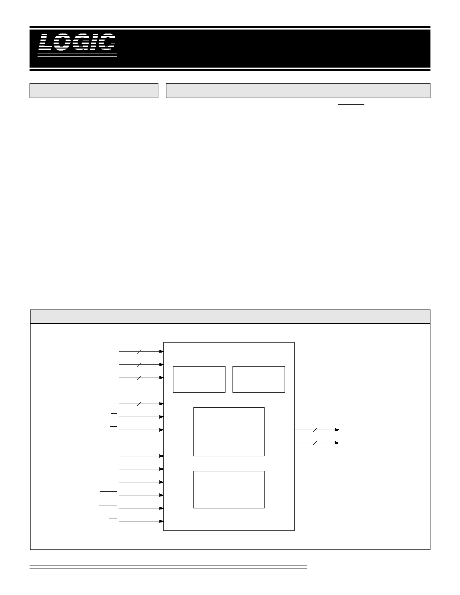
The LF48908 is a high-speed two
dimensional convolver that imple-
ments a 3 x 3 kernel convolution at
real-time video rates. Programmable
row buffers are located on-chip,
eliminating the need for external data
storage. Each row buffer can store up
to 1024 pixels. Two internal register
banks are provided allowing two
separate sets of filter coefficients to be
stored simultaneously. Adaptive filter
operations are possible when both
register banks are used. An on-chip
ALU is provided, allowing real-time
arithmetic and logical pixel point
operations to be performed on the
image data. The 3 x 3 convolver
comprises nine 8 x 8-bit multipliers,
various pipeline registers, and sum-
mers. A complete sum-of-products
operation is performed every clock
cycle. The FRAME signal resets all
data registers without affecting the
control and coefficient registers.
Pixel and coefficient input data are
both 8-bits and can be either signed or
unsigned integers. Image data should
be in a raster scan non-interlaced
format. The LF48908 can internally
store images as wide as 1024 pixels for
the 3 x 3 convolution. By using
external row buffers and multiple
LF48908s, longer pixel rows can be
used and convolutions with larger
kernel sizes can be performed. Out-
put data is 20-bits and this guarantees
no overflow for kernel sizes up to 4 x 4.
A separate cascade input is used as
the data input for summing results
from multiple LF48908s. It can also
function as the data input path when
external line buffers are used.
F
IGURE
1.
LF48908 B
LOCK
D
IAGRAM
DIN
7-0
CIN
9-0
CASO
7-0
A
2-0
LD
CS
CASI
15-0
CLK
HOLD
FRAME
RESET
OE
DOUT
19-0
16
3
8
8
20
8
EALU
3 x 3
CONVOLVER
ALU
ROW
BUFFERS
CONTROL
LOGIC
DEVICES INCORPORATED
LF48908
Two Dimensional Convolver
2
Video Imaging Products
08/9/2000≠LDS.48908-J
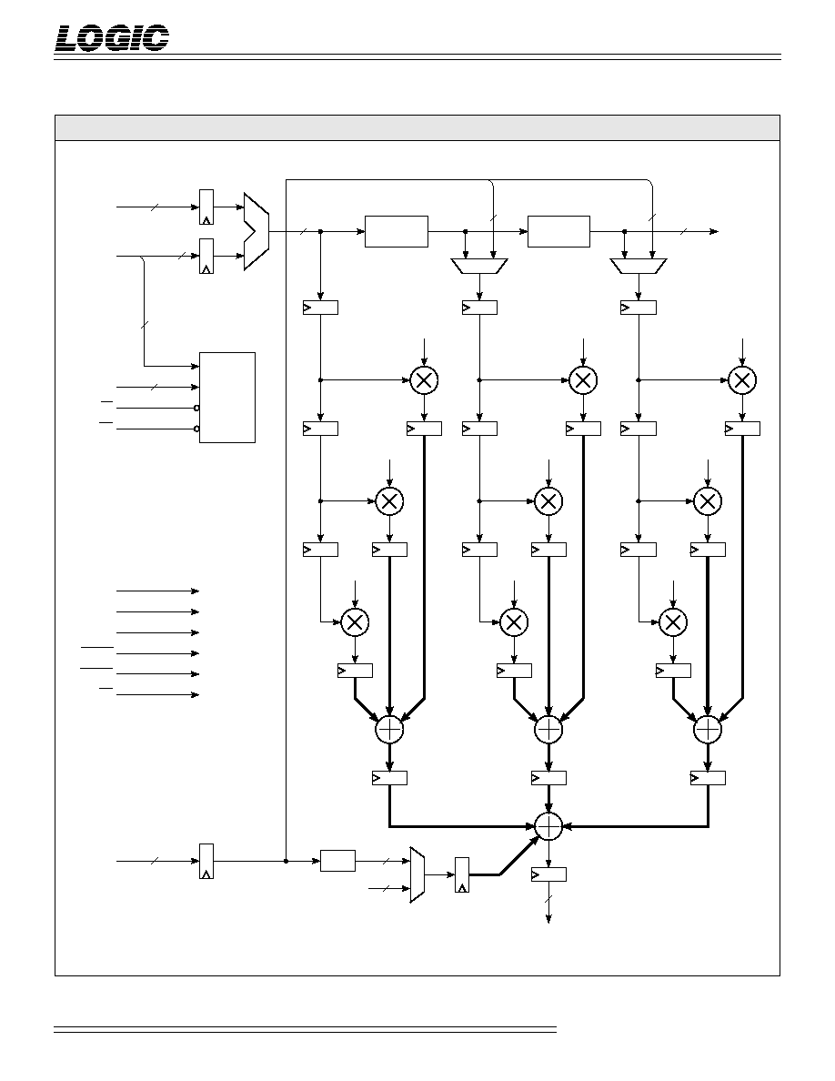
F
IGURE
2.
LF48908 F
UNCTIONAL
B
LOCK
D
IAGRAM
DIN
7-0
1-4
CIN
9-0
2:1
2:1
ROW
BUFFER
ROW
BUFFER
CASO
7-0
7-0
15-8
A
2-0
LD
CS
CONTROL
LOGIC
CASI
15-0
2:1
SHIFT
0
CLK
HOLD
FRAME
RESET
OE
DOUT
19-0
I
H
G
F
E
D
C
B
A
ALU
REGISTER
ALU
20
20
16
3
8
8
10
20
8
8
8
8
7-0
EALU
NOTE: NUMBERS IN REGISTER INDICATE
NUMBER OF PIPELINE DELAYS.

DEVICES INCORPORATED
3
LF48908
Two Dimensional Convolver
1
2
3
4
5
6
7
8
9
10
11
08/9/2000≠LDS.48908-J
Video Imaging Products
A
2-0
-- Control Logic Address Lines
A
2-0
determines which Control Logic
Register will receive the CIN
9-0
data.
CS -- Chip Select
When CS is LOW, data can be loaded
into the Control Logic Registers.
When CS is HIGH, data can not be
loaded and the register contents will
not be changed.
LD -- Load Strobe
If CS and LD are LOW, the data
present on CIN
9-0
will be latched into
the Control Logic Register addressed
by A
2-0
on the rising edge of LD.
FUNCTIONAL DESCRIPTION
The LF48908, a two-dimensional
convolver, executes convolutions using
internal row buffers to reduce design
complexity and board space require-
ments. 8-bit image data, in raster scan,
non-interlace format, is convolved with
one of two internal, 3 x 3 user-
programable filter kernels. Two 1024 x 8-
bit row buffers provide the data delay
needed to perform two-dimensional
convolutions on a single chip. The result
output of 20-bits allows for word growth
during the convolution operation.
The input data path (DIN
7-0
) provides
access to an 8-bit ALU. This allows
point operations to be performed on
the incoming data stream before
reaching the row buffers and the
convolver. The length of these buffers
is programmable for use in various
video formats without the need for
additional external delay.
This device is configured by loading
the coefficent data (filter kernels) and
row buffer length through the
coefficent data path (CIN
7-0
). Internal
registers are addressed using the A
2-0
address lines. Chip Select (CS) and
Load Strobe (LD) complete the
configuration interface which may be
controlled by standard microproces-
sors without additional external logic.
SIGNAL DEFINITIONS
Power
V
CC
and GND
+5 V power supply. All pins must be
connected.
Clock
CLK -- Master Clock
The rising edge of CLK strobes all
enabled registers except for the
Control Logic Registers.
Inputs
DIN
7-0
-- Pixel Data Input
DIN
7-0
is the 8-bit registered pixel
data input port. Data is latched on the
rising edge of CLK.
CIN
9-0
-- Coefficient and Control Logic
Register Input
CIN
7-0
is used to load the Coefficient
Registers or can be used to provide a
second operand input to the ALU.
CIN
8-0
is used to load the Initializa-
tion Register. CIN
9-0
is used to load
the ALU Microcode and Row Buffer
Length Registers. The Control Regis-
ter Address Lines, A
2-0
, determine
which register will receive the CIN
data. The CIN data is loaded into the
addressed register by using the CS
and LD control inputs.
CASI
15-0
-- Cascade Input
The cascade input is used when
multiple LF48908s are cascaded
together or when external row buffers
are needed. This allows convolutions
of larger kernels or longer row sizes.
Outputs
DOUT
19-0
-- Data Output
DOUT
19-0
is the 20-bit registered data
output port.
CASO
7-0
-- Cascade Output
The data presented on CASO
7-0
is the
internal ALU output delayed by twice
the programmed internal row buffer
length.
Controls
RESET -- Reset Control
When RESET is LOW, all internal
circuitry is reset, all outputs are forced
LOW, all Control Logic Registers are
loaded with their default values
(which is 0 for each one except the
ALU Microcode Register which has a
default value of "0000011000"), and all
other internal registers are loaded
with a "0".
FRAME -- New Frame Input Control
When asserted, FRAME signals the
start of a new frame. When FRAME is
LOW, all internal circuitry is reset
except for the ALU Microcode, Row
Length, Initialization, Coefficient, and
ALU Registers.
EALU -- Enable ALU Register Input
When HIGH, data on CIN
7-0
is latched
into the ALU Register on the next
rising edge of CLK. When LOW, data
on CIN
7-0
will not be latched into the
ALU Register and the register con-
tents will not be changed.
HOLD -- Hold Control
The HOLD input is used to disable
CLK from all of the internal circuitry.
HOLD is latched on the rising edge of
CLK and takes effect on the next rising
edge of CLK. When HOLD is HIGH,
CLK will have no effect on the
LF48908 and all internal data will
remain unchanged.
OE -- Output Enable
When OE is LOW, DOUT
19-0
is
enabled for output. When OE is
HIGH, DOUT
19-0
is placed in a high-
impedance state.

DEVICES INCORPORATED
LF48908
Two Dimensional Convolver
4
Video Imaging Products
08/9/2000≠LDS.48908-J
The filtered image data is output on
the Data Output bus (DOUT
19-0
). This
bus is registered with three-state
drivers to facilatate use on a standard
microprocessor system bus.
Data Input
Image data is input to the 3 x 3
convolver using DIN
7-0
. Data present
on DIN
7-0
is latched into a program-
mable pipeline delay on the rising
edge of CLK. The programmable
pipeline delay (1 to 4 clock cycles)
allows for synchronization of input
data when multiple LF48908s are
cascaded together to perform larger
convolutions. This delay is pro-
gramed via the Initialization Register
(see Table 3). The image data format,
unsigned or two's complement, is also
controlled by this register.
Coefficient data is input to the 3 x 3
convolver using either of two Coef-
ficient Registers (CREG
0
or CREG
1
).
The Coefficient Registers are loaded
through CIN
7-0
using the A
2-0
, CS, and
LD controls. The coefficient data
format, unsigned or two's comple-
ment, is determined by the Initializa-
tion Register.
Arithmetic Logic Unit
The input data path ALU with shifter
allows pixel point operations to be
performed on the incoming image.
These operations include arithmetic
functions, logical masking, and left/
right shifts. The 10-bit ALU Micro-
code Register controls the various
operations. The three upper bits
control the shift amount and direction
while the seven lower bits determine
the arithmetic or logical operation.
The shift operation is performed on
the output of the ALU. This shift
operation is independent of the
arithmetic or logical operation of the
ALU.
Tables 1 and 2 show the operations of
the ALU Microcode Register. The "A"
operand comes from the DIN input
data path, while the "B" operand is
taken from the ALU Register. The
ALU Register is loaded using CIN
7-0
and EALU. With EALU HIGH, data
from CIN
7-0
is loaded into the ALU
Register on the rising edge of CLK.
With EALU LOW, the data is held in
the ALU Register. Since CIN
7-0
is also
used to load the Control Logic Regis-
ters, it is possible to overwrite data in
those registers if CS and LD are active
when loading the ALU Register.
Therefore, special care must be taken
to ensure that CS and LD are not
active when writing to the ALU
Register.
Programmable Row Buffers
The two internal row buffers provide
the delay needed to perform the two-
dimensional convolution. The row
buffers function like 8-bit serial shift
registers with a user-programmable
delay from 1 to 1024 stages (it is
possible to select delay stages of 1 or
2, but this leads to meaningless results
for a 3 x 3 kernel convolution). The
row buffer length is set via the Row
Length Register (see Row Length
Register Section). The row buffers are
connected in series to provide the
proper pixel information to the
multiplier array. The Cascade Output
(CASO
7-0
) provides a 2X row delay of
the input data allowing for cascading
of LF48908s to handle larger frames
and/or kernel sizes. If more than 1024
delay stages are needed, it is possible
to use external row buffers and bypass
the internal row buffers. Bit 0 of the
Initialization Register determines if
internal or external row buffers are
used. If Bit 0 is a "0", the internal row
buffers are used. If Bit 0 is a "1", the
internal row buffers are bypassed and
external row buffers may be used.
3 x 3 Multiplier Array
The multiplier array comprises nine
8 x 8-bit multipliers. The active
Coefficient Register supplies the
coefficents to each of the multipliers,
while the pixel data comes from the
data input path and row buffers. The
array forms a sum-of-products result
as defined by the equation listed in
Figure 3.
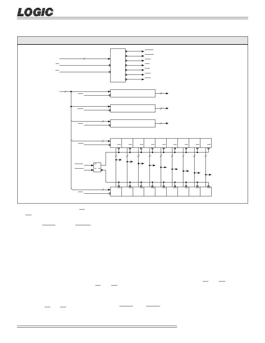
CONTROL LOGIC
Four sets of registers, the ALU Micro-
code, Row Length, Initialization, and
Coefficient, define the Control Logic
section. These registers are updated
F
IGURE
3.
M
ULTIPLIER
A
RRAY
O
UTPUT
P1
P2
P3
P4
P5
P6
P7
P8
P9
A
B
C
D
E
F
G
H
I
PIXEL INPUT DATA
FILTER KERNEL
MULTIPLIER ARRAY OUTPUT
A(P1)
=
+ D(P4)
+ G(P7)
+
+
+
B(P2)
E(P5)
H(P8)
+
+
+
C(P3)
F(P6)
I(P9)
DEVICES INCORPORATED
5
LF48908
Two Dimensional Convolver
1
2
3
4
5
6
7
8
9
10
11
08/9/2000≠LDS.48908-J
Video Imaging Products
Row Length Register
The value stored in the Row Length
Register determines the number of
delay stages for each row buffer. The
number of delay stages should be set
equal to the row length of the input
image. The Row Length Register may
be loaded with the values 0 through
1023 (0 represents 1024 delay stages).
It is possible to program the row
buffers to have 1 or 2 delay stages, but
this will lead to meaningless results
for a 3 x 3 convolution. This register is
loaded through CIN
9-0
using the A
2-0
,
CS, and LD controls. Once the Row
Length Register has been loaded, a
new value can not be loaded until the
LF48908 has been reset. This is done
by asserting RESET. After RESET goes
HIGH, the Row Length Register must
be loaded within 1024 CLK cycles. If
the Row Length Register is not loaded
within 1024 CLK cycles, the register
will automatically be loaded with a "0".
Initialization Register
The Initialization Register configures
various functions of the device
including: input data delay, input
data format, coefficent data format,
output rounding, cascade mode, and
cascade input shift (see Table 3). This
register is loaded through CIN
8-0
using the A
2-0
, CS, and LD controls.
Coefficient Registers - CREG
0
, CREG
1
The Coefficient Registers are used to
store the filter coefficients for the
multiplier array. Each Coefficient
through the CIN bus using A
2-0
, CS,
and LD (see Figure 4). All the Control
Logic Registers are set to their default
values when RESET is active. FRAME
does not affect the values in these
registers.
ALU Microcode Register
Operation of the ALU and shifter are
determined by the value stored in the
ALU Microcode Register. This 10-bit
instruction word is divided into two
fields. The lower seven bits define the
arithmetic and logical operations of the
ALU. The upper three bits specify shift
distance and direction. Tables 1 and 2
detail the various instruction words.
This register is loaded through CIN
9-0
using the A
2-0
, CS, and LD controls.
Also see Arithmetic Logic Unit section.
F
IGURE
4.
LF48908 C
ONTROL
L
OGIC
B
LOCK
D
IAGRAM
A
2-0
LD
CS
ADDRESS
DECODE
3
ENCR
1
ENCR
0
CAS
CR
1
CR
0
LMC
EOR
CIN
9-0
10
ALU MICROCODE REGISTER
LMC
ALU MICROCODE
10
ROW LENGTH REGISTER
EOR
ROW LENGTH
10
INITIALIZATION REGISTER
CAS
INITIALIZATION DATA
9
8-0
I
0
H
0
G
0
F
0
E
0
D
0
C
0
B
0
A
0
CR
0
CR
1
S
R
Q
Q
OE
OE
OE
OE
OE
OE
OE
OE
OE
I
1
H
1
G
1
F
1
E
1
D
1
C
1
B
1
A
1
OE
OE
OE
OE
OE
OE
OE
OE
OE
ENCR
1
ENCR
0
I
H
G
F
E
D
C
B
A
8
8
8
8
8
8
8
8
8
COEFFICIENT REGISTER 0
COEFFICIENT REGISTER 1
9
7-0
8
7-0
8