 | –≠–ª–µ–∫—Ç—Ä–æ–Ω–Ω—ã–π –∫–æ–º–ø–æ–Ω–µ–Ω—Ç: LMS12C-65 | –°–∫–∞—á–∞—Ç—å:  PDF PDF  ZIP ZIP |
DEVICES INCORPORATED
LMS12
12-bit Cascadable Multiplier-Summer
Multiplier-Summers
08/16/2000≠LDS.S12-J
1
u
u
u
u
u 12 x 12-bit Multiplier with
Pipelined 26-bit Output Summer
u
u
u
u
u Summer has 26-bit Input Port Fully
Independent from Multiplier
Inputs
u
u
u
u
u Cascadable to Form Video Rate FIR
Filter with 3-bit Headroom
u
u
u
u
u A, B, and C Input Registers Sepa-
rately Enabled for Maximum
Flexibility
u
u
u
u
u 28 MHz Data Rate for FIR Filtering
Applications
u
u
u
u
u High Speed, Low Power CMOS
Technology
u
u
u
u
u 84-pin PLCC, J-Lead
FEATURES
DESCRIPTION
LMS12
12-bit Cascadable Multiplier-Summer
DEVICES INCORPORATED
The LMS12 is a high-speed 12 x 12-bit
combinatorial multiplier integrated
with a 26-bit adder in a single 84-pin
package. It is an ideal building block
for the implementation of very high-
speed FIR filters for video, RADAR,
and other similar applications. The
LMS12 implements the general form
(A
∑
B) + C. As a result, it is also useful
in implementing polynomial approxi-
mations to transcendental functions.
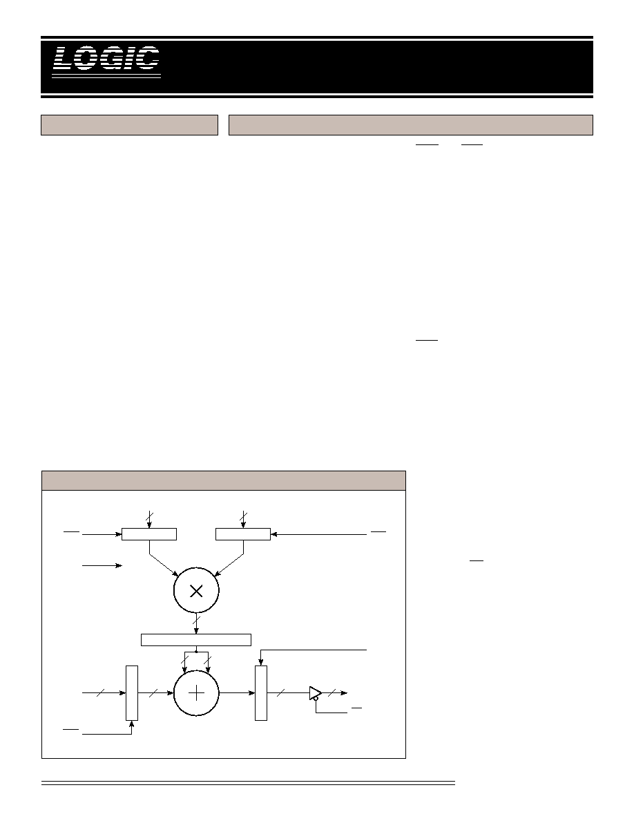
ARCHITECTURE
A block diagram of the LMS12 is
shown below. Its major features are
discussed individually in the follow-
ing paragraphs.
MULTIPLIER
The A
11-0
and B
11-0
inputs to the
LMS12 are captured at the rising edge
of the clock in the 12-bit A and B input
registers, respectively. These registers
are independently enabled by the
ENA and ENB inputs. The registered
input data are then applied to a
12 x 12-bit multiplier array, which
produces a 24-bit result. Both the
inputs and outputs of the multiplier
are in two's complement format. The
multiplication result forms the input
to the 24-bit product register.
SUMMER
The C
25-0
inputs to the LMS12 form a
26-bit two's complement number
which is captured in the C register at
the rising edge of the clock. The C
register is enabled by assertion of the
ENC input. The summer is a 26-bit
adder which operates on the C
register data and the sign extended
contents of the product register to
produce a 26-bit sum. This sum is
applied to the 26-bit S register.
OUTPUT
The FTS input is the feedthrough
control for the S register. When FTS is
asserted, the summer result is applied
directly to the S output port. When
FTS is deasserted, data from the S
register is output on the S port,
effecting a one-cycle delay of the
summer result. The S output port can
be forced to a high-impedance state by
driving the OE control line high. FTS
would be asserted for conventional
FIR filter applications, however the
insertion of zero-coefficient filter taps
may be accomplished by negating
FTS. Negating FTS also allows
application of the same filter transfer
function to two interleaved datas-
treams with successive input and
output sample points occurring on
alternate clock cycles.
LMS12 B
LOCK
D
IAGRAM
CLK
A REGISTER
B REGISTER
ENA
ENB
ENC
12
24
A
11-0
B
11-0
PRODUCT REGISTER
24
2
C REGISTER
S REGISTER
26
C
25-0
26
26
26
OE
S
25-0
FTS
12
SIGN
EXTENDED
DEVICES INCORPORATED
LMS12
12-bit Cascadable Multiplier-Summer
Multiplier-Summers
08/16/2000≠LDS.S12-J
2
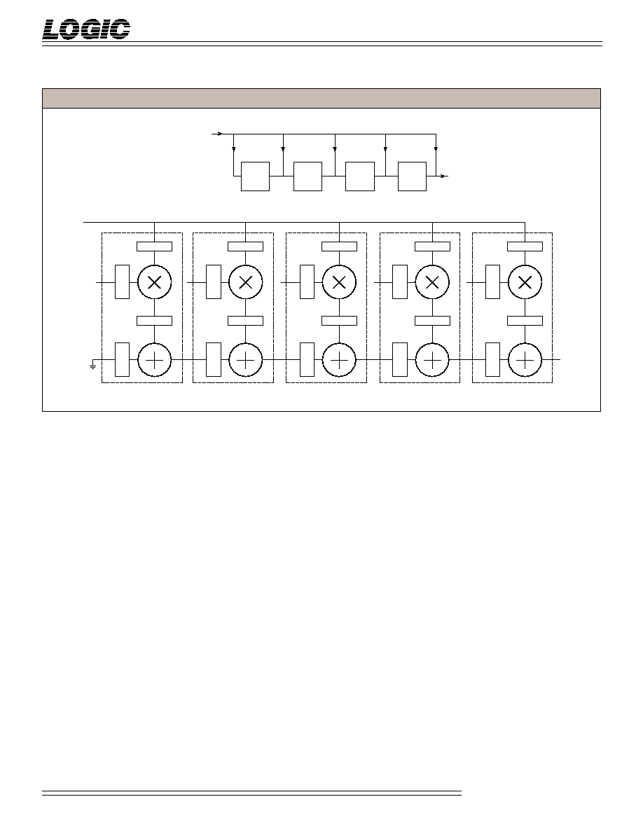
F
IGURE
1.
F
LOW
D
IAGRAM
FOR
5-T
AP
FIR F
ILTER
A
3
h
3
A
4
h
4
Z
≠1
A
2
h
2
A
1
h1
h
0
y(n)
x(n)
y(n)
h
0
h
1
h
2
h
3
h
4
x(n)
Z
≠1
Z
≠1
Z
≠1
Z
≠1
Z
≠1
Z
≠1
Z
≠1
Z
≠1
A
0
APPLICATIONS
The LMS12 is designed specifically for
high-speed FIR filtering applications
requiring a throughput rate of one
output sample per clock period. By
cascading LMS12 units, the transpose
form of the FIR transfer function is
implemented directly, with each of the
LMS12 units supplying one of the
filter weights, and the cascaded
summers accumulating the results.
The signal flow graph for a 5-tap FIR
filter and the equivalent implementa-
tion using LMS12's is shown in
Figure 1.
The operation of the 5-tap FIR filter
implementation of Figure 1 is depicted
in Table 1. The filter weights h
4
- h
0
are assumed to be latched in the B
input registers of the LMS12 units.
The x(n) data is applied in parallel to
the A input registers of all devices.
For descriptive purposes in the table,
the A register contents and sum
output data of each device is labelled
according to the index of the weight
applied by that device; i.e., S
0
is
produced by the rightmost device,
which has h
0
as its filter weight and
A
0
as its input register contents. Each
column represents one clock cycle,
with the data passing a particular
point in the system illustrated across
each row.
DEVICES INCORPORATED
LMS12
12-bit Cascadable Multiplier-Summer
Multiplier-Summers
08/16/2000≠LDS.S12-J
3
CLK Cycle
1
2
3
4
5
6
7
8
9
X
(n)
X
n
X
n+1
X
n+2
X
n+3
X
n+4
X
n+5
X
n+6
X
n+7
X
n+8
A
4
Register
X
n
X
n+1
X
n+2
X
n+3
X
n+4
X
n+5
X
n+6
X
n+7
Sum 4
h
4
X
n
h
4
X
n+1
h
4
X
n+2
h
4
X
n+3
h
4
X
n+4
h
4
X
n+5
h
4
X
n+6
A
3
Register
X
n
X
n+1
X
n+2
X
n+3
X
n+4
X
n+5
X
n+6
X
n+7
Sum 3
h
3
X
n
h
3
X
n+1
h
3
X
n+2
h
3
X
n+3
h
3
X
n+4
h
3
X
n+5
h
3
X
n+6
+ h
4
X
n≠1
+ h
4
X
n
+ h
4
X
n+1
+ h
4
X
n+2
+ h
4
X
n+3
+ h
4
X
n+4
+ h
4
X
n+5
A
2
Register
X
n
X
n+1
X
n+2
X
n+3
X
n+4
X
n+5
X
n+6
X
n+7
Sum 2
h
2
X
n
h
2
X
n+1
h
2
X
n+2
h
2
X
n+3
h
2
X
n+4
h
2
X
n+5
h
2
X
n+6
+ h
3
X
n≠1
+ h
3
X
n
+ h
3
X
n+1
+ h
3
X
n+2
+ h
3
X
n+3
+ h
3
X
n+4
+ h
3
X
n+5
+ h
4
X
n≠2
+ h
4
X
n≠1
+ h
4
X
n
+ h
4
X
n+1
+ h
4
X
n+2
+ h
4
X
n+3
+ h
4
X
n+4
A
1
Register
X
n
X
n+1
X
n+2
X
n+3
X
n+4
X
n+5
X
n+6
X
n+7
Sum 1
h
1
X
n
h
1
X
n+1
h
1
X
n+2
h
1
X
n+3
h
1
X
n+4
h
1
X
n+5
h
1
X
n+6
+ h
2
X
n≠1
+ h
2
X
n
+ h
2
X
n+1
+ h
2
X
n+2
+ h
2
X
n+3
+ h
2
X
n+4
+ h
2
X
n+5
+ h
3
X
n≠2
+ h
3
X
n≠1
+ h
3
X
n
+ h
3
X
n+1
+ h
3
X
n+2
+ h
3
X
n+3
+ h
3
X
n+4
+ h
4
X
n≠3
+ h
4
X
n≠2
+ h
4
X
n≠1
+ h
4
X
n
+ h
4
X
n+1
+ h
4
X
n+2
+ h
4
X
n+3
A
0
Register
X
n
X
n+1
X
n+2
X
n+3
X
n+4
X
n+5
X
n+6
X
n+7
Sum 0
h
0
X
n
h
0
X
n+1
h
0
X
n+2
h
0
X
n+3
h
0
X
n+4
h
0
X
n+5
h
0
X
n+6
+ h
1
X
n≠1
+ h
1
X
n
+ h
1
X
n+1
+ h
1
X
n+2
+ h
1
X
n+3
+ h
1
X
n+4
+ h
1
X
n+5
+ h
2
X
n≠2
+ h
2
X
n≠1
+ h
2
X
n
+ h
2
X
n+1
+ h
2
X
n+2
+ h
2
X
n+3
+ h
2
X
n+4
+ h
3
X
n≠3
+ h
3
X
n≠2
+ h
3
X
n≠1
+ h
3
X
n
+ h
3
X
n+1
+ h
3
X
n+2
+ h
3
X
n+3
+ h
4
X
n≠4
+ h
4
X
n≠3
+ h
4
X
n≠2
+ h
4
X
n≠1
+ h
4
X
n
+ h
4
X
n+1
+ h
4
X
n+2
T
ABLE
1.
T
IMING
E
XAMPLE
FOR
5-T
AP
N
ONDECIMATING
FIR F
ILTER
F
IGURE
2
B
.
O
UTPUT
F
ORMATS
23 22 21
14 13 12
2
1
2
0
2
≠1
2
≠8
2
≠9
2
≠10
11 10 9
2
1
0
2
≠11
2
≠12
2
≠13
2
≠20
2
≠21
2
≠22
Fractional Two's Complement
23 22 21
14 13 12
2
23
2
22
2
21
2
14
2
13
2
12
11 10 9
2
1
0
2
11
2
10
2
9
2
2
2
1
2
0
Integer Two's Complement
25 24
25 24
≠2
3
(Sign)
2
2
≠2
25
(Sign)
2
24
F
IGURE
2
A
.
I
NPUT
F
ORMATS
11 10 9
2
1
0
≠2
0
(Sign)
2
≠1
2
≠2
2
≠9
2
≠10
2
≠11
11 10 9
2
1
0
≠2
0
(Sign)
2
≠1
2
≠2
2
≠9
2
≠10
2
≠11
Fractional Two's Complement
11 10 9
2
1
0
≠2
11
(Sign)
2
10
2
9
2
2
2
1
2
0
11 10 9
2
1
0
≠2
11
(Sign)
2
10
2
9
2
2
2
1
2
0
Integer Two's Complement
A
IN
B
IN

DEVICES INCORPORATED
LMS12
12-bit Cascadable Multiplier-Summer
Multiplier-Summers
08/16/2000≠LDS.S12-J
4
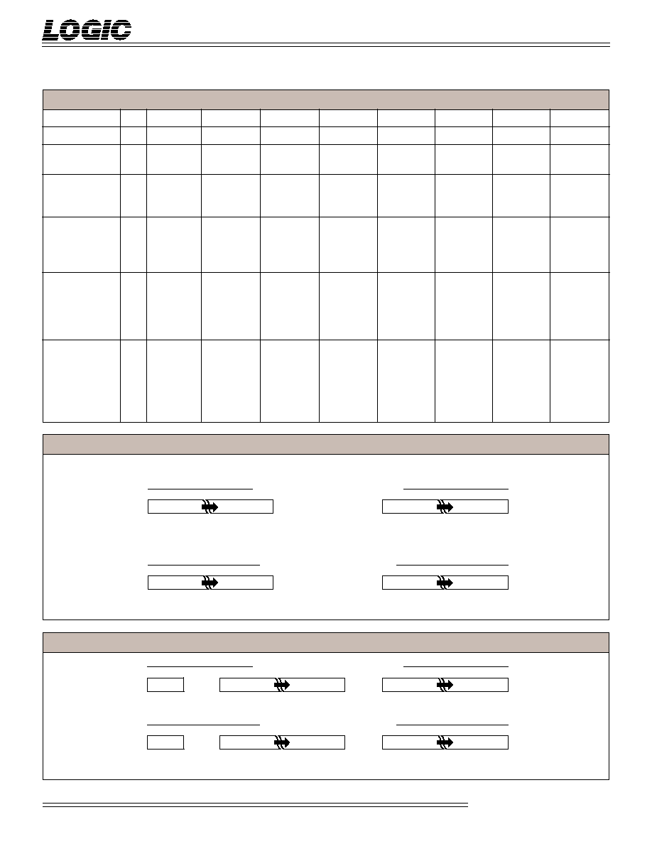
Symbol
Parameter
Test Condition
Min
Typ
Max
Unit
V
OH
Output High Voltage
V
CC
= Min., I
OH
= ≠2.0 mA
2.4
V
V
OL
Output Low Voltage
V
CC
= Min., I
OL
= 4.0 mA
0.5
V
V
IH
Input High Voltage
2.0
V
CC
V
V
IL
Input Low Voltage
(Note 3)
0.0
0.8
V
I
IX
Input Current
Ground
V
IN
V
CC
(Note 12)
±
20
µA
I
OZ
Output Leakage Current
Ground
V
OUT
V
CC
(Note 12)
±
20
µA
I
CC1
V
CC
Current, Dynamic
(Notes 5, 6)
15
25
mA
I
CC2
V
CC
Current, Quiescent
(Note 7)
1.0
mA
Storage temperature ........................................................................................................... ≠65∞C to +150∞C
Operating ambient temperature ........................................................................................... ≠55∞C to +125∞C
V
CC
supply voltage with respect to ground ............................................................................ ≠0.5 V to +7.0 V
Input signal with respect to ground ........................................................................................ ≠3.0 V to +7.0 V
Signal applied to high impedance output ............................................................................... ≠3.0 V to +7.0 V
Output current into low outputs ............................................................................................................. 25 mA
Latchup current ............................................................................................................................... > 400 mA
M
AXIMUM
R
ATINGS
Above which useful life may be impaired (Notes 1, 2, 3, 8)
O
PERATING
C
ONDITIONS
To meet specified electrical and switching characteristics
E
LECTRICAL
C
HARACTERISTICS
Over Operating Conditions (Note 4)
Mode
Temperature Range (Ambient)
Supply
Voltage
Active Operation, Commercial
0∞C to +70∞C
4.75 V
V
CC
5.25 V
Active Operation, Military
≠55∞C to +125∞C
4.50 V
V
CC
5.50 V

DEVICES INCORPORATED
LMS12
12-bit Cascadable Multiplier-Summer
Multiplier-Summers
08/16/2000≠LDS.S12-J
5
12345678901234567890123
12345678901234567890123
12345678901234567890123
12345678901234567890123
12345678901234567890123
12345678901234567890123
12345678901234567890123
12345678901234567890123
12345678901234567890123
12345678901234567890123
12345678901234567890123
12345678901234567890123
12345678901234567890123
12345678901234567890123
12345678901234567890123
12345678901234567890123
12345678901234567890123
12345678901234567890123
12345678901234567890123
12345678901234567890123
12345678901234567890123
12345678901234567890123
12345678901234567890123
12345678901234567890123
12345678901234567890123
12345678901234567890123
12345678901234567890123
12345678901234567890123
12345678901234567890123
12345678901234567890123
12345678901234567890123
12345678901234567890123
12345678901234567890123
12345678901234567890123
12345678901234567890123
12345678901234567890123
12345678901234567890123
12345678901234567890123
12345678901234567890123
12345678901234567890123
12345678901234567890123
12345678901234567890123
12345678901234567890123
12345678901234567890123
12345678901234567890123
LMS12≠
65*
50*
40
35
Symbol
Parameter
Min
Max
Min
Max
Min
Max
Min
Max
t
CP
Clock Period
40
35
30
25
t
PW
Clock Pulse Width
15
15
12
8
t
SAB
A, B, Data Setup Time
15
12
12
10
t
SC
C Data Setup Time
15
10
7
7
t
SEN
ENA, ENB, ENC Setup Time
15
12
12
10
t
HAB
A, B, Data Hold Time
5
5
5
2
t
HC
C Data Hold Time
5
5
5
2
t
HEN
ENA, ENB, ENC Hold Time
5
5
5
2
t
D
Clock to S≠FT = 1
50
40
35
30
Clock to S≠FT = 0
25
25
25
20
t
ENA
Three-State Output Enable Delay
(Note 11)
25
25
25
20
t
DIS
Three-State Output Disable Delay
(Note 11)
22
22
22
20
C
OMMERCIAL
O
PERATING
R
ANGE
(0∞C to +70∞C)
Notes 9, 10 (ns)
SWITCHING CHARACTERISTICS
S
WITCHING
W
AVEFORMS
HIGH IMPEDANCE
INPUTS
A, B, C
t
ENA
t
DIS
t
PW
t
SAB
t
SC
t
SEN
ENA
ENB, ENC
CLOCK
OE
t
D
S OUTPUTS
t
HEN
t
PW
R OUTPUTS
t
HAB
t
HC
123456789012345678901234
123456789012345678901234
123456789012345678901234
123456789012345678901234
*D
ISCONTINUED
S
PEED
G
RADE