
LESHAN RADIO COMPANY, LTD.
S29≠1/2
High-speed diode
SOD523 SC-79
1
2
BAS516
2
ANODE
1
CATHODE
LIMITING VALUES In accordance with the Absolute Maximum Rating System (IEC 134).
SYMBOL
PARAMETER
CONDITIONS
MIN.
MAX.
UNIT
V
RRM
repetitive peak reverse voltage
≠
85
V
V
R
continuous reverse voltage
≠
75
V
I
F
continuous forward current
T
s
=90∞C; note 1; see Fig.1
≠
250
mA
I
FRM
repetitive peak forward current
≠
500
mA
I
FSM
non-repetitive peak forward current
square wave; T
j
=25∞C prior to
surge; see Fig.3
t =1
µ
s
≠
4
A
t =1 ms
≠
1
A
t =1 s
≠
0.5
A
P
tot
total power dissipation
T
s
=90∞C; note 1
≠
500
mW
T
stg
storage temperature
-65
+150
∞C
T
j
junction temperature
≠
150
∞C
Note
1. Ts is the temperature at the soldering point of the cathode tab.
ELECTRICAL CHARACTERISTICS T
j
=25∞C unless otherwise specified.
SYMBOL
PARAMETER
CONDITIONS
MAX.
UNIT
V
F
forward voltage
see Fig.2 I
F
= 1 mA
715
mV
I
F
= 10 mA
855
mV
I
F
=50 mA
1
V
I
F
= 150 mA
1.25
V
I
R
reverse current
see Fig.4 V
R
= 25 V
30
nA
V
R
=75 V
1
µ
A
V
R
= 25 V; T
j
= 150 ∞C
30
µ
A
V
R
= 75 V; T
j
= 150 ∞C;
50
µ
A
C
d
diode capacitance
f = 1 MHz; V
R
= 0; see Fig.5
1
pF
t
rr
reverse recovery time
when switched from I
F
=10mA to I
R
= 10mA;
4
n s
R
L
= 100
; measured at I
R
= 1 mA; see Fig.6
V
fr
forward recovery voltage
when switched from IF = 10 mA; tr = 20 ns; see Fig.7
1.75
V
THERMAL CHARACTERISTICS
SYMBOL
PARAMETER
CONDITIONS
VALUE
UNIT
R
th j-s
thermal resistance from junction to soldering point
note 1
120
K/W
Note 1. Soldering point of the cathode tab.
FEATURES
∑ Ultra small plastic SMD package
∑ High switching speed: max. 4 ns
∑ Continuous reverse voltage: max. 75 V
∑ Repetitive peak reverse voltage: max. 85 V
∑ Repetitive peak forward current: max. 500 mA.
APPLICATIONS
∑ High-speed switching in e.g. surface mounted
circuits.
DESCRIPTION
The BAS516 is a high-speed
switching diode fabricated in
planar technology, and
encapsulated in the SOD523
(SC79) SMD plastic package.
LESHAN RADIO COMPANY, LTD.
S29≠2/2
500
400
300
200
100
0
0
1
2
T
S
(
∞C
)
300
200
100
0
0
50
100
150
200
V
F
( V )
I
F
(mA)
0.6
0.4
0.2
0
0
100
200
T
J
( ∞C )
I
R
(nA)
C
d
(pF)
0
4
8
12
16
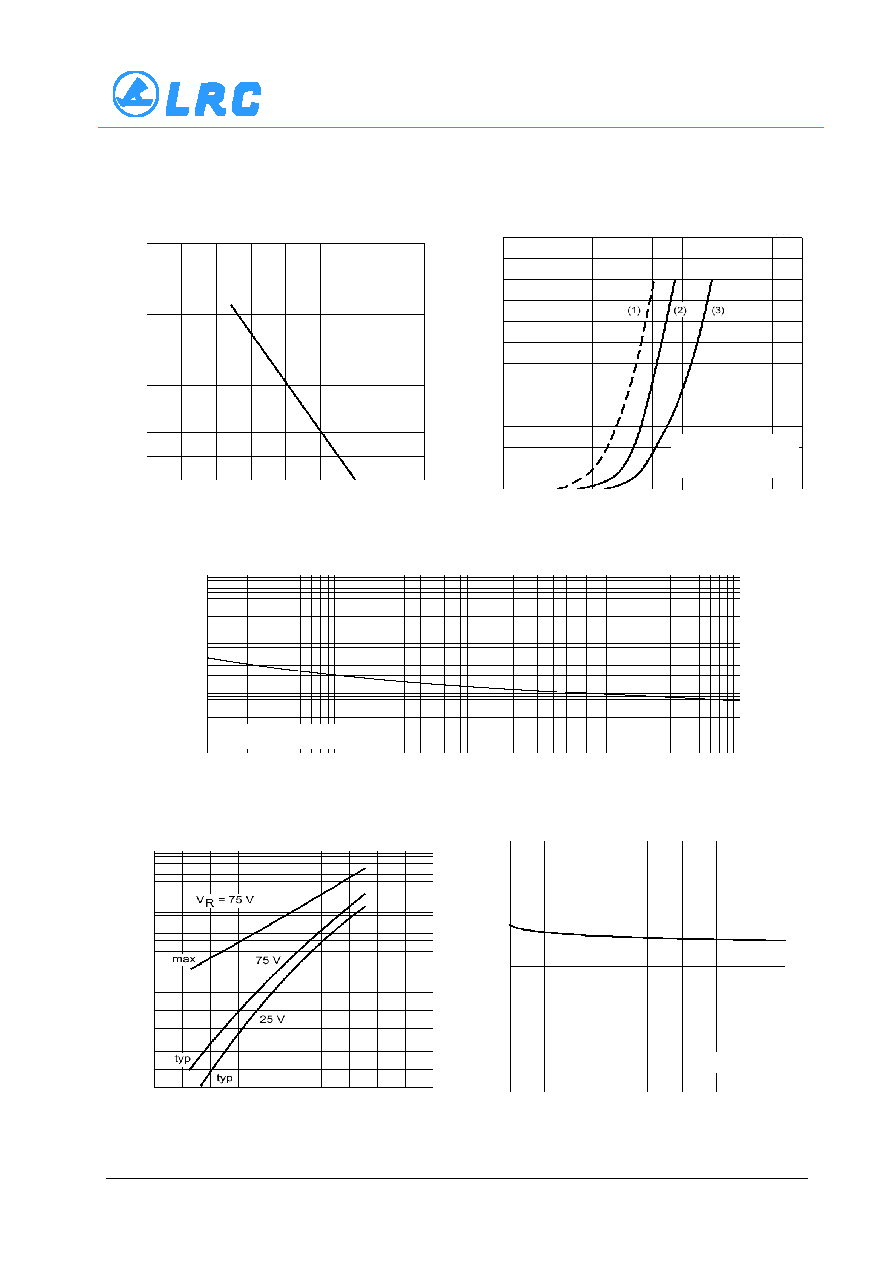
Fig.1 Maximum permissible continuous forward current as a
function of soldering point temperature.
Fig.2 Forward current as a function of
forward voltage.
(1) T
j
= 150 ∞C; typical values.
(2)T
j
=25∞C; typical values.
(3) T
j
=25∞C; maximum values.
I
F
(mA)
Fig.3 Maximum permissible non-repetitive peak forward current as a function of pulse duration.
Based on square wave currents;
T
j
=25∞C prior to surge.
t
P
(
µ
s
)
I
FSM
(A)
10
2
10
1
10
-1
0
10
10
2
10
3
10
4
10
5
10
4
10
3
10
2
10
V
R
( V )
f = 1 MHz ; T
j
=25∞C;
Fig.4 Reverse current as a function of junction
temperature.
Fig.5 Diode capacitance as a function of
reverse voltage; typical values.
BAS516
LESHAN RADIO COMPANY, LTD.
S29≠3/2
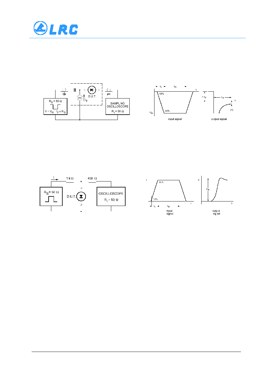
BAS516
(1) I
R
= 1 mA.
Input signal: reverse pulse rise time t
r
= 0.6 ns; reverse voltage pulse duration t
p
= 100 ns; duty factor
= 0.05;
Oscilloscope: rise time t
r
= 0.35 ns.
Fig.6 Reverse recovery voltage test circuit and waveforms.
Input signal: forward pulse rise time
t
r
= 20 ns; forward current pulse duration
t
p
100 ns; duty factor
0.005.
Fig.7 Forward recovery voltage test circuit and waveforms.