LESHAN RADIO COMPANY, LTD.
LDTA
143EET1-1/3
Bias Resistor Transistors
PNP Silicon Surface Mount Transistors
with Monolithic Bias Resistor Network
This new series of digital transistors is designed to replace a single
device and its external resistor bias network. The BRT (Bias Resistor
Transistor) contains a single transistor with a monolithic bias network
consisting of two resistors; a series base resistor and a base-emitter
resistor. The BRT eliminates these individual components by integrating
them into a single device. The use of a BRT can reduce both system
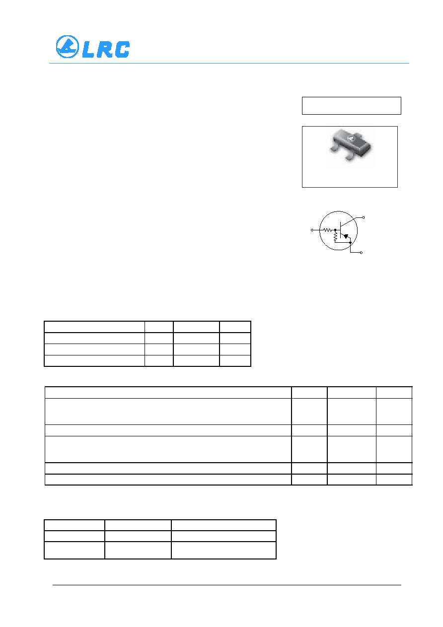
cost and board space. The device is housed in the SC-89 package
which is designed for low power surface mount applications.
LDTA143EET1
∑ Simplifies Circuit Design
∑ Reduces Board Space
∑ Reduces Component Count
∑ The SC-89 package can be soldered using wave or reflow. The
modified gull-winged leads absorb thermal stress during soldering
eliminating the possibility of damage to the die.
∑ Pb-Free Package is Available.
1
3
2
SC-89
MAXIMUM RATINGS
(T
A
= 25
∞
C unless otherwise noted)
Rating
Symbol
Value
Unit
Collector-Base Voltage
V
CBO
50
Vdc
Collector-Emitter Voltage
V
CEO
50
Vdc
Collector Current
I
C
100
mAdc
PIN 3
COLLECTOR
(OUTPUT)
PIN 2
EMITTER
(GROUND)
PIN 1
BASE
(INPUT)
R
1
R
2
THERMAL CHARACTERISTICS
Characteristic
Symbol
Max
Unit
Total Device Dissipation,
FR≠4 Board (Note 1.) @ TA = 25
∞
C
Derate above 25
∞
C
PD
200
1.6
mW
mW/
∞
C
Thermal Resistance, Junction to Ambient (Note 1.)
R
JA
600
∞
C/W
Total Device Dissipation,
FR≠4 Board (Note 2.) @ TA = 25
∞
C
Derate above 25
∞
C
PD
300
2.4
mW
mW/
∞
C
Thermal Resistance, Junction to Ambient (Note 2.)
R
JA
400
∞
C/W
Junction and Storage Temperature Range
TJ, Tstg
≠55 to +150
∞
C
1. FR≠4 @ Minimum Pad
2. FR≠4 @ 1.0
◊
1.0 Inch Pad
DEVICE MARKING AND ORDERING INFORMATION
Device
Marking
Shipping
LDTA143EET1
6J
3000/Tape&Reel
LDTA143EET1G
6J
(Pb-Free)
3000/Tape&Reel
LESHAN RADIO COMPANY, LTD.
LDTA143EET1-2/3
L
DTA143EET1
ELECTRICAL CHARACTERISTICS
(T
A
= 25
∞
C unless otherwise noted) (Continued)
Characteristic
Symbol
Min
Typ
Max
Unit
OFF CHARACTERISTICS
Collector-Base Cutoff Current (V
CB
= 50 V, I
E
= 0)
I
CBO
≠
≠
100
nAdc
Collector-Emitter Cutoff Current (V
CE
= 50 V, I
B
= 0)
I
CEO
≠
≠
500
nAdc
Emitter-Base Cutoff Current
(V
BE
= 6.0 V)
I
EBO
≠
≠
1.5
mAdc
Collector-Base Breakdown Voltage (I
C
= 10
µ
A, I
E
= 0)
V
(BR)CBO
50
≠
≠
Vdc
Collector-Emitter Breakdown Voltage (Note 3)
(I
C
= 2.0 mA, I
B
= 0)
V
(BR)CEO
50
≠
≠
Vdc
ON CHARACTERISTICS
(Note 3)
DC Current Gain
(V
CE
= 10 V, I
C
= 5.0 mA)
h
FE
15
≠
Collector-Emitter Saturation Voltage (I
C
= 10 mA, I
B
= 1 mA)
V
CE(sat)
≠
≠
0.25
Vdc
(V
CC
= 5.0 V, V
B
= 2.5 V, R
L
= 1.0 k
)
V
OL
≠
≠
0.2
Vdc
3. Pulse Test: Pulse Width < 300
µ
s, Duty Cycle < 2.0%
Output Voltage (on)
3.3
4.7 6.1
Resistor Ratio
R
1
/R
2
0.8 1.0 1.2
Input Resistor
R
1
k
(V
CC
= 5.0 V, V
B
= 0.25 V, R
L
= 1.0 k
)
Output Voltage (off)
V
OH
≠
≠
Vdc
4.9
27

LESHAN RADIO COMPANY, LTD.
G
M
0.08 (0.003)
X
D
3 PL
J
-X-
-Y-
NOTES:
1. DIMENSIONING AND TOLERANCING PER ANSI
Y14.5M, 1982.
2. CONTROLLING DIMENSION: MILLIMETERS
3. MAXIMUM LEAD THICKNESS INCLUDES LEAD
FINISH THICKNESS. MINIMUM LEAD THICKNESS
IS THE MINIMUM THICKNESS OF BASE
MATERIAL.
4. 463C-01 OBSOLETE, NEW STANDARD 463C-02.
A
B
Y
1
2
3
N
2 PL
K
C
-T-
SEATING
PLANE
DIM
A
MIN
NOM
MIN
NOM
INCHES
1.50
1.60
1.70
0.059
MILLIMETERS
B
0.75
0.85
0.95
0.030
C
0.60
0.70
0.80
0.024
D
0.23
0.28
0.33
0.009
G
0.50 BSC
H
0.53 REF
J
0.10
0.15
0.20
0.004
K
0.30
0.40
0.50
0.012
L
1.10 REF
M
---
---
10
---
N
---
---
10
---
S
1.50
1.60
1.70
0.059
0.063
0.067
0.034
0.040
0.028
0.031
0.011
0.013
0.020 BSC
0.021 REF
0.006
0.008
0.016
0.020
0.043 REF
---
10
---
10
0.063
0.067
MAX
MAX
_
_
_
_
M
H
H
L
G
RECOMMENDED PATTERN
OF SOLDER PADS
S
SC-8
9
LDTA143EET1
LDTA143EET1≠3/3