 | –≠–ª–µ–∫—Ç—Ä–æ–Ω–Ω—ã–π –∫–æ–º–ø–æ–Ω–µ–Ω—Ç: LS7055 | –°–∫–∞—á–∞—Ç—å:  PDF PDF  ZIP ZIP |
6 DECADE PREDETERMINING UP/DOWN COUNTER
FEATURES:
∑ +4.75V to +15V (Vss - V
DD
)
∑ Preset, Presignal and Mainsignal Store
∑ DC to 250kHz Count Frequency
∑ Fully Synchronous Operation
Three Comparators with Output Flags
Automatic or Manual Preset/Reset Control
∑ Thumbwheel Interface for Storage Selects
∑ Prescale on Count Input Selectable
∑ Count Inhibit
∑ Up/Down Control
∑ Scan Rate up to 150kHz
∑ Scan Oscillator has Override Capability
∑ Blanking Override for Decimal Point Operaton
∑ Multiplexed 7 Segment and BCD Data Output
∑ Output latches
∑ Reset
∑ Hysteresis on Count Input
∑ CMOS Type Noise Immunity on all other inputs
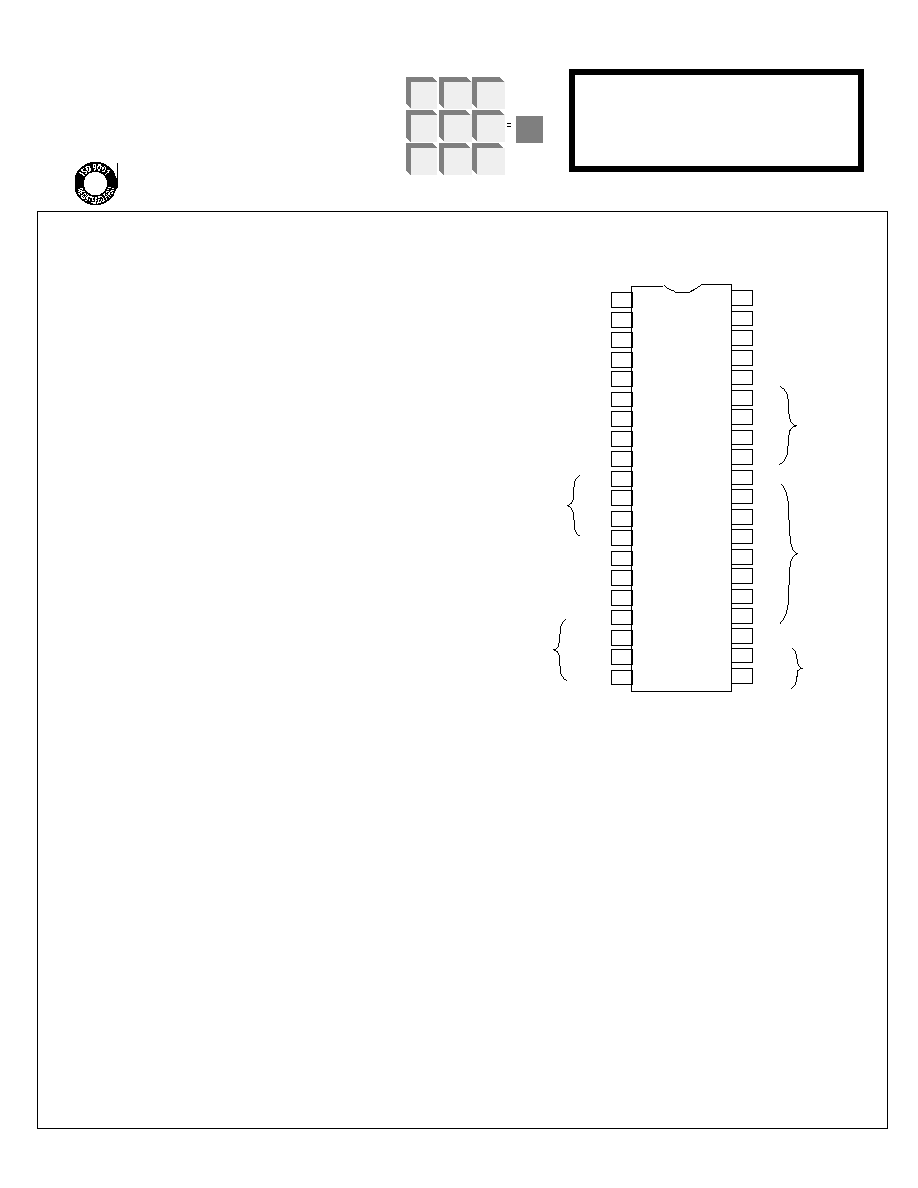
∑ LS7055, LS7056 (DIP) - See Figure 1
DESCRIPTION:
The LS7055/LS7056 is a MOS synchronous 6 decade Up/Down
counter. The circuit includes storages and comparators, zero de-
tect, automatic presetting and resetting, output latches, multi-
plexed output BCD and seven segment data. Thumbwheel
switches can be used to provide BCD data to the storage net-
works in the circuit.
COUNT (Pin 40)
Counter operates at speeds up to 250kHz and advances on the
positive edge of the input count pulse.
UP/DOWN (Pin 39)
Counter operates in up or down mode. A high input causes the
counter to operate in the up mode while a low input causes it to
operate in the down mode.
COUNT INHIBIT (Pin 1)
A high input inhibits counting and the counter remains at its last
count. A low input enables counting.
DATA TRANSFER INPUT (Pin 37)
A high input allows the seven segment display and BCD data to
follow the count (the internal latches become transparent). A low
input prevents updating of the latches as the count advances and
the seven segment display and BCD data outputs remain fixed.
RESET (Pin 4)
A high input resets and holds all counter stages at zero. A low
input allows counter operation.
January 2003
7055-012703-1
LSI/CSI
LSI Computer Systems, Inc. 1235 Walt Whitman Road, Melville, NY 11747 (631) 271-0400 FAX (631) 271-0405
LS7055
LS7056
LSI
1
2
3
4
5
6
7
8
9
10
11
12
13
14
15
16
17
18
19
20
21
22
23
24
25
26
27
28
29
30
31
32
33
34
35
36
37
38
39
40
FIGURE 1
PIN ASSIGNMENT - TOP VIEW
COUNT INPUT
UP/DOWN INPUT
ZERO DETECT OUTPUT
DATA TRANSFER INPUT
PRESIGNAL OUTPUT
B1
B2
B4
B8
BLANKING OVERRIDE
g
f
e
V
SS
(+V)
c
b
LSD
V
DD
(-V)
RESET INPUT
COUNT INHIBIT INPUT
DIVIDE CONTROL INPUT 1
DIVIDE CONTROL INPUT 2
MAIN SIGNAL OUTPUT
B8
B4
B2
B1
BCD
DATA
O U T P U T S
DIGIT
S E L E C T
O U T P U T S
L S 7 0 5 5
S E G M E N T
O U T P U T S
INHIBIT INTERNAL RESET INPUT
INHIBIT INTERNAL PRESET INPUT
P R E S E T I N P U T
BCD
DATA
INPUTS
SELECT STORAGE INPUT 1
SELECT STORAGE INPUT 2
L S D + 1
L S D + 2
L S D + 3
L S D + 4
SCAN OSCILLATOR INPUT
MSD
a
d
*
OPTIONAL CHOICE-LAMP TEST (SPECIFY LS7056)
DIGIT
S E L E C T
O U T P U T S
INHIBIT INTERNAL RESET (Pin 5)
A high input prevents the automatic reset of the counter to zero when
in the up mode and when the counter reaches the number in the
main signal store.
PRESET (Pin 7)
A high level presets the BCD counter to the number set in the preset
store. A low input allows counter operation.
INHIBIT INTERNAL PRESET (Pin 6)
A high input prevents the automatic preset of the counter to the
number set in preset store when in the down mode and the counter
reaches zero.
SELECT STORAGE OF DATA INPUTS (Pins 15, 16)
Two inputs which allow BCD data to be stored in either the preset,
presignal or main signal store. The proper method for loading the
stores is depicted in Figure 4.
PIN 15
PIN16
STORAGE
0
0
No Selection
1
0
Presignal
0
1
Main Signal
1
1
Preset
UL
Æ
A3800
*

LAMP TEST (LS7056 only) (Pin 31)
A high input will cause the seven segment outputs to provide all 8's
to a display (BCD outputs are not affected).
ZERO DETECT OUTPUT (Pin 38)
A high output occurs whenever the counter is at zero. In the auto-
matic mode and with the Up/Down input in the down mode, the
counter presets to the number in the preset store and the zero
detect output is typically a 1.5 µs pulse. In the manual mode
(inhibit internal preset is high), the counter remains at zero until a
preset or a count input pulse is applied.
DIGIT SELECT OUTPUTS (Pins 17, 18, 19, 20, 21, 22)
Six positive outputs for digit identification. The outputs occur
sequentially going from MSD to LSD and can be applied directly to
thumbwheel switches. They must be buffered before being applied
to the seven segment displays either by a CMOS or transistor buf-
fer as shown in Figure 5. Figure 3 indicates the timing relationship
between the digit select outputs and the BCD data outputs.
SEVEN SEGMENT OUTPUTS (Pins 24, 25, 26, 27, 28, 29, 30)
Capable of sourcing current into the base of a common emitter
NPN transistor for interfacing to a seven segment display. Small
displays needing an average current of 0.5 mA can be interfaced
to the circuit without external transistors. A typcial example of a
12V circuit is shown in Figure 5.
BCD OUTPUTS (Pins 32, 33, 34, 35)
Four outputs corresponding to the BCD data stored in the latches.
The outputs can be demultiplexed using the circuitry shown in Fig-
ure 4. As can be seen from the timing diagram of Figure 3, the
BCD data output and seven segment outputs are completely
stable during the positive digit select outputs.
POWER-ON-RESET
An external RC network applied to the reset input as shown in Fig-
ure 4 can be used to reset the counter to zero upon application of
power. The preset input must be held low at this time. The RC time
constant should be larger than the power supply rise time. For ex-
ample, a 100k
resistor and a 0.1µF capacitor could be used if the
power supply rise time was 5 ms.
POWER SUPPLIES
The circuit operates over the range of +4.75V to +15V. At +4.75V,
the inputs are TTL and CMOS compatible (external pull-up re-
sistors must be provided on any input which does not pull up to
Vss) when using TTL inputs. At +15V, inputs are CMOS compat-
ible. All outputs are CMOS compatible from +4.75V to +15V.
BCD DATA INPUTS (Pins 10, 11, 12, 13)
Four inputs containing BCD data which are applied to either the
preset, presignal or main signal stores one decade at a time. This
data can be provided by a set of thumbwheel switches which are
driven by the digit select outputs. Referring to Figure 4, the BCD
data inputs have built in pull down resistors (typically 51k Ohms).
DIVIDE CONTROL (Pin 2, Pin 3)
Two inputs for selection to divide the count input by either 5, 6 or 1.
PIN 2
PIN 3
0
0
Divide by 5
1
0
Divide by 6
1
1
Divide by 1
MAIN SIGNAL OUTPUT (Pin 9)
An internal comparator provides a high level output when the num-
ber set into the main signal store is reached by the counter. In the
automatic mode and with the Up/Down control in the up position,
the counter is reset to zero and the main signal output is typically a
2.5 µs wide pulse. In the manual mode (inhibit internal reset is high)
the output remains high until the next count input or a reset is ap-
plied.
PRESIGNAL OUTPUT (Pin 36)
The presignal comparator provides a high level output when the
number set into the presignal storage is reached. The output re-
mains high until the next count input or a reset or preset is applied.
SCAN CLOCK INPUT (Pin 23)
A DC to 150kHz oscillator input port for driving the internal scan
counter is provided. Up to 150kHz may be used when de-
multiplexilng BCD data using the digit select outputs. The fre-
quency of the oscillator is determined by an external RC network as
shown in Figure 4. Table 1 indicates several frequencies and their
associated RC networks. The oscillator can be overridden using an
external driver. Table 2 indicates the external drive requriements.
When displaying, leading zero blanking and unblanking on LSD is
provided.
BLANKING OVERRIDE (LS7055 only) (Pin 31)
On circuits with this option, unblanking can be made to occur on
any digit by connecting that digit select output to the unblanking in-
put. Since the input has an internal pull down resistor, it can be left
floating when not in use.
TABLE 1
Typical resistor/capacitor values for the scan oscillator
RESISTOR CAPACITOR TYPICAL FREQUENCY
12k
1000pF
100kHz
100k
1000pF
10kHz
1.0M
1000pF
1kHz
TABLE 2
Driver Requirements for Overriding Scan Oscillator Input
Power Supply (V)
Sink Current
Source Current
5
1.0mA
0
10
4.5mA
0
15
10.0mA
0
7055-012703-2

MAXIMUM RATINGS
PARAMETER
SYMBOL
VALUE
UNITS
Storage Temperature
Tstg
-65 to +150
∞C
Operating Temperature T
A
-25 to +70
∞C
Voltage (any pin to Vss) Vmax
-30 to +0.5
V
DC ELECTRICAL CHARACTERISTICS
(V
DD
= V
GG
= 0V, Vss = +4.75 to +15V, -25∞C
T
A
+70∞C unless
otherwise specified.)
PARAMETER SYM MIN MAX UNITS
Quescent Supply Current
-
-
-
-
(All Input Pins Tied to Vss)
(All Output Pins Left Open)
Vss = 4.75V
I
DD
-
20
mA
Vss = 15V
I
DD
-
25
mA
Input Capacitance All Inputs
Cin
-
10
pF
Hysteresis On Count Input
30%(Vss - V
DD
)
-
V
Noise Immunity All Other Inputs
V
NL
30%(Vss - V
DD
)
-
V
V
NH
30%(Vss - V
DD
)
-
V
Output Levels All Outputs
V
OL
-
0.5
V
(All Output Pins Left Open)
V
OH
Vss - 1
-
V
7 Segment Output Current
Source Current
Vss = 4.75V, V
OUT
= 0.7V, 70∞C I
SEG
0.3
-
mA
Vss = 4.75V, V
OUT
= 0.7V, 25∞C I
SEG
0.4
-
mA
Vss = 10V, V
OUT
= 7V, 25∞C
I
SEG
2.0
-
mA
Vss = 15V, V
OUT
= 13V, 70∞C
I
SEG
3.0
-
mA
Note: Limit Segment Source Current to 4.5mA max.
Sink Current (V
OUT
= 0.4V)
Vss = 4.75V, 25∞C
I
SEG
-21
-
µA
Vss = 10V, 25∞C
I
SEG
-17
-
µA
Vss = 15V, 25∞C
I
SEG
-15
-
µA
Vss = 15V, 70∞C
I
SEG
-10
-
µA
BCD, Zero Detect, Mainsignal and Presignal Output Current
Source Current
Vss = 4.75V, V
OUT
= 4.5V, 70∞C Io
H
0.10
-
mA
Vss = 4.75V, V
OUT
= 4.5V, 25∞C Io
H
0.13
-
mA
Vss = 10V, V
OUT
= 9.0V, 25∞C
Io
H
0.7
-
mA
Vss = 15V, V
OUT
= 13V, 25∞C
Io
H
2.5
-
mA
Note: Limit Segment Source Current to 4.5mA max.
Sink Current (V
OUT
= 0.4V)
Vss = 4.75V, 25∞C
Io
L
-7.5
-
µA
Vss = 10V, 25∞C
Io
L
-6.0
-
µA
Vss = 15V, 25∞C
Io
L
-5.5
-
µA
Vss = 15V, 70∞C
Io
L
-4.0
-
µA
Digit Select Output Current
Source Current
Vss = 4.75V, V
OUT
= 4.5V, 70∞C Io
H
0.28
-
mA
Vss = 4.75V, V
OUT
= 4.5V, 25∞C Io
H
0.35
-
mA
Vss = 10V, V
OUT
= 9V, 25∞C
Io
H
2.0
-
mA
Vss = 15V, V
OUT
= 13.5V, 70∞C
Io
H
7.0
-
mA
Note: Limit digit select current to 10mA.
Sink Current (V
OUT
= 0.4V)
Vss = 4.75V, 25∞C
Io
L
-15
-
µA
Vss = 10V, 25∞C
Io
L
-12
-
µA
Vss = 15V, 25∞C
Io
L
-11
-
µA
Vss = 15V, 70∞C
Io
L
-
µA
DYNAMIC ELECTRICAL CHARACTERISTICS
(V
DD
= V
GG
= 0V, Vss = +4.75 to +15V, -25∞C
T
A
+70∞C
unless otherwise specified.)
PARAMETER
SYM
MIN
MAX
UNITS
Count Input Frequency
Vss = 4.75V
Fc
DC
250
kHz
Vss = 10V
Fc
DC
175
kHz
Vss = 15V
Fc
DC
125
kHz
Pulse Width
Vss = 4.75V
Tcw
2
-
µs
Vss = 10V
Tcw
2.8
-
µs
Vss = 15V
Tcw
4
-
µs
Rise Time
Tcr
-
µs
Fall Time
Tcf
-
µs
Scan Input Frequency
Fsc
DC 100
kHz
Divide Control
Set-Up Time
Tds
2
-
µs
Hold Time
Tdh
8
-
µs
Reset Pulse Width
**
Trpw
2
-
µs
Reset
Set Up Time
Trs
0
-
µs
Hold Time
Trh
6
-
µs
Inhibit Internal Reset
Set Up Time
Tis
0
-
µs
Hold Time
*
Tirh
3
-
µs
Preset Pulse Width
**
Tppw
2
-
µs
Preset Enable
Set Up Time
Tips
0
-
µs
Hold Time
*
Tiph
6
-
µs
Data Transfer Pulse Width
**
Tdtw
2
-
µs
Data Transfer
Set Up Time
Tdts
0
-
µs
Hold Time
Tdth
6
-
µs
Up/Down
Set Up Time
Tuds
0
-
µs
Hold Time
Tud 10
-
µs
Count Inhibit
Set Up Time
Tcs
2
-
µs
Hold Time
Tch 10
-
µs
Data Outputs (C
L
= 10pF)
Rise Time
Tdr
-
1.0
µs
Fall Time
Vss = 4.75V
Tdf
-
2.0
µs
Vss = 10V
Tdf
-
3.0
µs
Vss = 15V
Tdf
-
4.0
µs
Digit Select Outputs Guard Band Time
within 7 segment & BCD outputs
Tgb
0.5
-
µs
See Figure 3
Main Signal, Presignal, Zero Detect
Outputs delay with respect to positive
edge of Count Input
Tdo
-
3
µs
Set-Up and Hold times are defined with respect to positive edge of count
input except where indicated by asterisks.
*
Indicates a hold time which must last for at least one whole count cycle
plus 5µs past the next positive edge of count input.
**
Reset, Preset and Data Transfer Pulse Width is as specified except if
applied when a count input is going positive. In that case the set-up and
hold times govern.
7055-012703-3
The information included herein is believed to be
accurate and reliable. However, LSI Computer Systems,
Inc. assumes no responsibilities for inaccuracies, nor for
any infringements of patent rights of others which may
result from its use.
COUNTER AT
MAINSIGNAL VALUE
COUNTER AT
PRESIGNAL VALUE
COUNTER AT
Z E R O
MAINSIGNAL OUTPUT
PRESIGNAL OUTPUT
ZERO DETECT OUTPUT
MANUAL
R E S E T
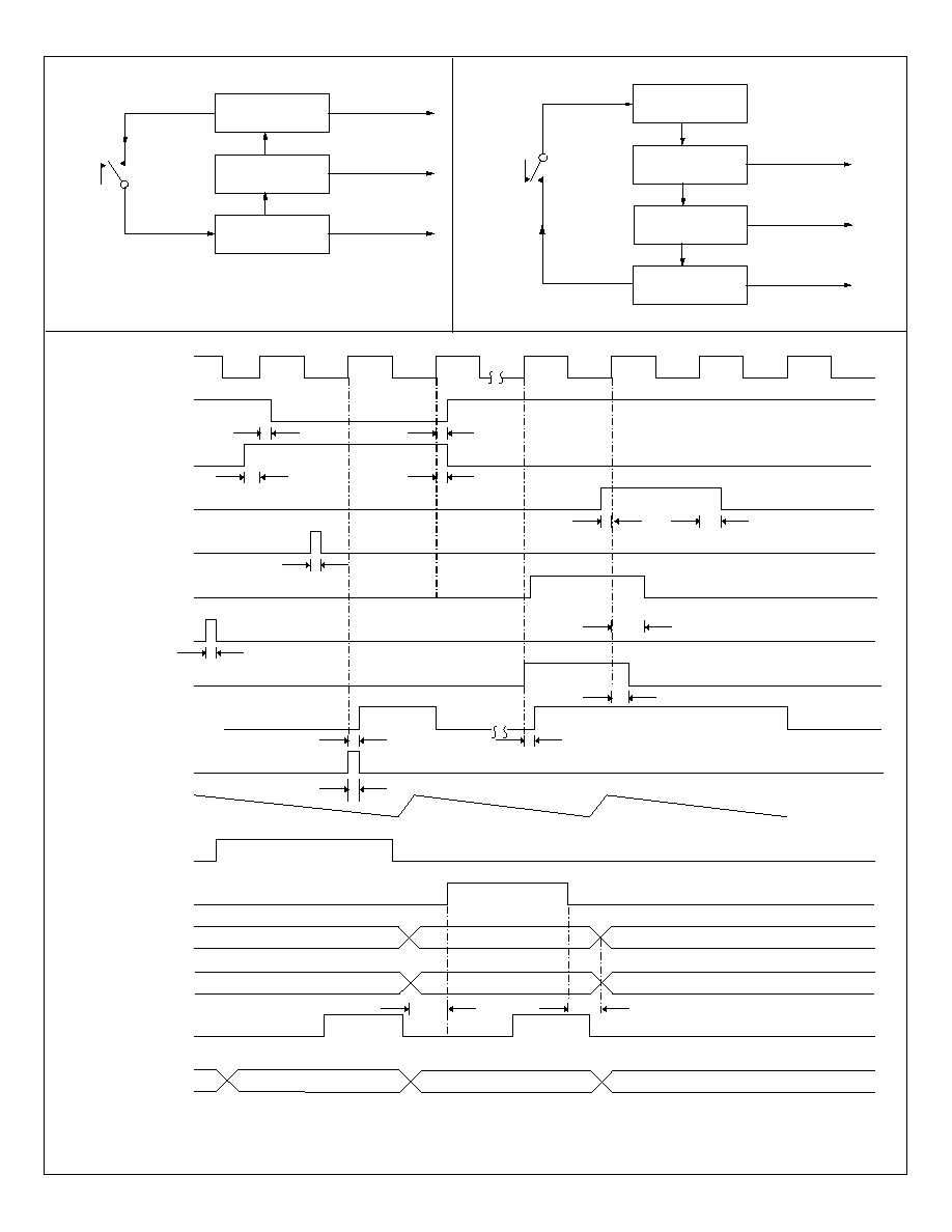
FIGURE 2. AUTOMATIC OR MANUAL OPERATION IN UP MODE
AUTOMATIC
R E S E T
COUNTER AT
P R E S E T N U M B E R
COUNTER AT
PRESIGNAL VALUE
COUNTER AT
Z E R O
MAINSIGNAL OUTPUT
PRESIGNAL OUTPUT
ZERO DETECT OUTPUT
MANUAL
P R E S E T
FIGURE 3. AUTOMATIC OR MANUAL OPERATION IN DOWN MODE
COUNTER AT
MAINSIGNAL
NUMBER
AUTOMATIC
P R E S E T
T
UDH
T
udh
T
ds
T
dh
T
cs
T
ch
T
rpw
T
ppw
T
do
T
do
T
gb
T
gb
T
dth
T
iph
COUNT INPUT
UP/DOWN
DIVIDE CONTROL
COUNT INHIBIT
RESET
INHIBIT
INTERNAL RESET
PRESET ENABLE
INHIBIT
INTERNAL PRESET
MAINSIGNAL, PRESIGNAL,
ZERO DETECT OUTPUT
DATA TRANSFER
INPUT
SCAN CLOCK
INPUT
MSD OUTPUT
LSD +4 OUTPUT
7 SEGMENTS
OUTPUTS
BCD OUTPUTS
STORAGE SELECT
INPUTS
BCD DATA
INPUT
*
FIGURE 4. TIMING DIAGRAM
*
BCD data input assumed to be applied from a set of thumbwheel switches as shown in Figure 5.
T
irh
7055-012703-4
7055-012703-5
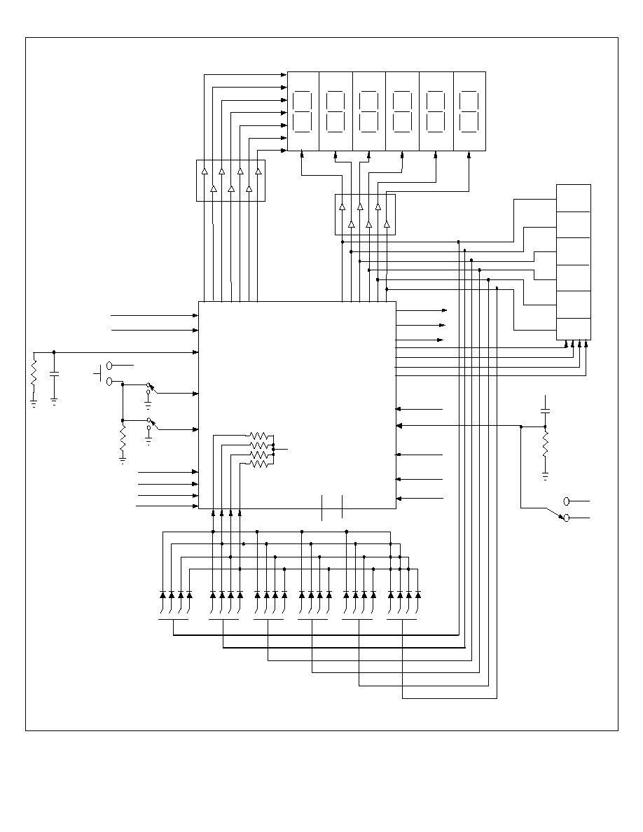
6 DIGIT
SELECT
OUTPUT
4 BCD DATA
OUTPUTS
MAINSIGNAL OUTPUT
PRESIGNAL OUTPUT
ZERO DETECT OUTPUT
RESET INPUT
INHIBIT INTERNAL
RESET INPUT
INHIBIT INTERNAL
PRESET INPUT
PRESET ENABLE
INPUT
UP/DOWN INPUT
7 SEGMENT OUTPUTS
DIVIDE CONTROL INPUTS
COUNT INPUT
COUNT INHIBIT
LOAD
COMMAND
Vss
BLANKING OVERRIDE
OR LAMP TEST
DATA TRANSFER INPUT
Vss
100k
(typical)
LE
LATCH ENABLE
LE
LE
LE
LE
Vss
Vss
V
DD
THUMBWHEEL SWITCHES
FIGURE 5. SYSTEM INTERCONNECTION DIAGRAM
BCD DATA INPUTS
BUFFER
BUFFER
LED DISPLAY
51K
V
DD
SELECT STORAGE
INPUTS
LS7055/LS7056
SCAN INPUT
1µF
(typical)
10k
EXT.
LATCH